

Page 1

MT7620
PROGRAMMING
GUIDE
Integrated 802.11n MAC/BBP and 2.4 GHz RF/FEM Router-on-a-Chip
Page 2
PGMT7620_V.1.0_040503
Page 2 of 523
MT7620 PROGRAMMING GUIDE
Integrated 802.11n MAC/BBP and 2.4 GHz RF/FEM Router-on-a-Chip
MIPS 24KEc
64 KB I-Cache
32 KB D-
Cache
(580 MHz)
OCP Bridge
OCP
_IF
Arbiter
DRAM
Controller
RBUS (SYS_CLK)
SPI
NFC
PBUS
GDMA
RJ45 x5
Switch
(4FE + 2GE)
5-Port EPHY
RGMII
TMII/MII
x2
PCIe 1.1
PHY
Single-Port
USB 2.0 PHY
Host/
Device
PCIe x1
UART
GPIO
PCM x4
I2S
I2C
I2S
PBUS
INTC
I2C
GPIO
/LED
SPI
NAND
UART
To CPU
interrupt
s
16-Bit
SDR/DDR1/DDR2
EJTAG
WLAN
11n 2x2
2.4 GHz
Timer
PCM
SDHC
SD
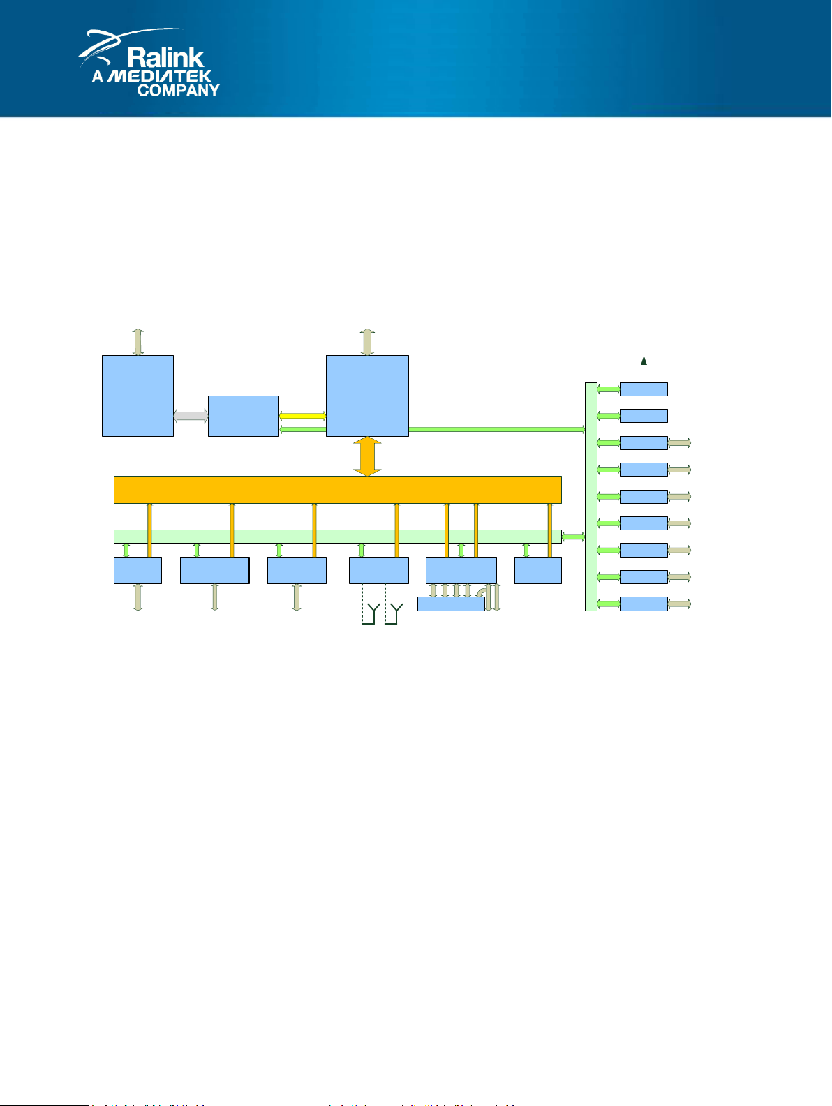
MT7620 Overview
The MT7620 SoC includes a high performance 580 MHz MIPS24KEc CPU core and USB host controller/PHY,
which is designed to enable a multitude of high performance, cost-effective IEEE 802.11n applications with a
MediaTek (Ralink) client card.
Functional Block Diagram
Figure 1-1 MT7620 Block Diagram
There are several masters (MIPS 24KEc, USB , PCI Express) in the MT7620 SoC on a high performance, low
latency Rbus, (Ralink Bus). In addition, the MT7620 SoC supports lower speed peripherals such as UART, GPIO,
and SPI via a low speed peripheral bus (Pbus). The SDRAM/DDR1/DDR2 controller is the only bus slave on the
Rbus. It includes an Advanced Memory Scheduler to arbitrate the requests from bus masters, enhancing the
performance of memory access intensive tasks.
Page 3

PGMT7620_V.1.0_040503
Page 3 of 523
MT7620 PROGRAMMING GUIDE
Integrated 802.11n MAC/BBP and 2.4 GHz RF/FEM Router-on-a-Chip
Table of Contents
1. MIPS 24K PROCESSOR 11
1.1 FEATURES 11
1.2 BLOCK DIAGRAM 12
1.3 MEMORY MAP SUMMARY 13
1.4 CLOCK PLAN 14
1.5 CPU CLOCK MUX 15
2. REGISTERS 16
2.1 NOMENCLATURE 16
2.2 SYSTEM CONTROL 17
2.2.1 FEATURES 17
2.2.2 BLOCK DIAGRAM 17
2.2.3 LIST OF REGISTERS 18
2.2.4 REGISTER DESCRIPTIONS (BASE: 0X1000_0000) 19
2.3 TIMER 46
2.3.1 FEATURES 46
2.3.2 BLOCK DIAGRAM 47
2.3.3 LIST OF REGISTERS 48
2.3.4 REGISTER DESCRIPTIONS (BASE: 0X1000_0100) 49
2.4 INTERRUPT CONTROLLER 53
2.4.1 FEATURES 53
2.4.2 BLOCK DIAGRAM 53
2.4.3 LIST OF REGISTERS 54
2.4.4 REGISTER DESCRIPTIONS (BASE: 0X1000_0200) 55
2.5 SYSTEM TICK COUNTER 60
2.5.1 LIST OF REGISTERS 60
2.5.2 REGISTER DESCRIPTIONS (BASE: 0X1000_0D00) 61
2.6 UART 62
2.6.1 FEATURES 62
2.6.2 BLOCK DIAGRAM 62
2.6.3 LIST OF REGISTERS 63
2.6.4 REGISTER DESCRIPTIONS (BASE: 0X1000_0500) 64
2.7 UART LITE 72
2.7.1 FEATURES 72
2.7.2 BLOCK DIAGRAM 72
2.7.3 LIST OF REGISTERS 73
2.7.4 REGISTER DESCRIPTIONS (BASE: 0X1000_0C00) 74
2.8 PROGRAMMABLE I/O 81
2.8.1 FEATURES 81
2.8.2 BLOCK DIAGRAM 81
2.8.3 LIST OF REGISTERS 82
2.8.4 REGISTER DESCRIPTIONS (BASE: 0X1000_0600) 84
2.9 I2C CONTROLLER 97
2.9.1 FEATURES 97
2.9.2 BLOCK DIAGRAM 97
2.9.3 LIST OF REGISTERS 98
Page 4

PGMT7620_V.1.0_040503
Page 4 of 523
MT7620 PROGRAMMING GUIDE
Integrated 802.11n MAC/BBP and 2.4 GHz RF/FEM Router-on-a-Chip
2.9.4 REGISTER DESCRIPTIONS (BASE: 0X1000_0900) 99
2.10 NAND FLASH CONTROLLER 105
2.10.1 FEATURES 105
2.10.2 NORMAL MODE FLOW 105
2.10.3 ECC 105
2.10.4 LIST OF REGISTERS 108
2.10.5 REGISTER DESCRIPTIONS (BASE: 0X1000_0800) 109
2.11 PCM CONTROLLER 116
2.11.1 FEATURES 116
2.11.2 BLOCK DIAGRAM 116
2.11.3 LIST OF REGISTERS 118
2.11.4 REGISTER DESCRIPTIONS (BASE: 0X1000_2000) 119
2.11.5 PCM CONFIGURATION 130
2.12 GENERIC DMA CONTROLLER 132
2.12.1 FEATURES 132
2.12.2 BLOCK DIAGRAM 132
2.12.3 PERIPHERAL CHANNEL CONNECTION 133
2.12.4 LIST OF REGISTERS 134
2.12.5 REGISTER DESCRIPTIONS (BASE: 0X1000_2800) 135
2.13 SPI CONTROLLER 139
2.13.1 FEATURES 139
2.13.2 BLOCK DIAGRAM 139
2.13.3 LIST OF REGISTERS 140
2.13.4 REGISTER DESCRIPTIONS (BASE: 0X1000_0B00) 141
2.14 I2S CONTROLLER 152
2.14.1 FEATURES 152
2.14.2 BLOCK DIAGRAM 152
2.14.3 I2S SIGNAL TIMING FOR I2S DATA FORMAT 153
2.14.4 LIST OF REGISTERS 154
2.14.5 REGISTER DESCRIPTIONS (BASE: 0X1000_0A00) 155
2.15 MEMORY CONTROLLER 159
2.15.1 FEATURES 159
2.15.2 BLOCK DIAGRAM 159
2.15.3 SDRAM INITIALIZATION SEQUENCE 159
2.15.4 SDRAM POWER SAVING CONFIGURATION 160
2.15.5 DDR INITIALIZATION SEQUENCE 161
2.15.6 LIST OF REGISTERS 162
2.15.7 REGISTER DESCRIPTIONS (BASE: 0X1000_0300) 163
2.16 RBUS MATRIX AND QOS ARBITER 178
2.16.1 FEATURES 178
2.16.2 BLOCK DIAGRAM 178
2.16.3 LIST OF REGISTERS 179
2.16.4 REGISTER DESCRIPTIONS (BASE: 0X1000_0400) 180
2.17 USB HOST CONTROLLER & PHY 183
2.17.1 FEATURES 183
2.17.2 BLOCK DIAGRAM 183
2.17.3 REGISTER DESCRIPTION (BASE: 0X101C.0000) 183
2.17.4 EHCI OPERATION REGISTERS (BASE: 0X101C.0000) 184
Page 5

PGMT7620_V.1.0_040503
Page 5 of 523
MT7620 PROGRAMMING GUIDE
Integrated 802.11n MAC/BBP and 2.4 GHz RF/FEM Router-on-a-Chip
2.17.5 OHCI OPERATION REGISTERS (BASE: 0X101C.1000) 185
2.18 USB DEVICE CONTROLLER 186
2.18.1 FEATURES 186
2.18.2 BLOCK DIAGRAM 186
2.18.3 BULK OUT 186
2.18.4 LEGACY MODE 187
2.18.5 AGGREGATION MODE 187
2.18.6 DE-AGGREGATION MODE 188
2.18.7 BULK-OUT AGGREGATION FORMAT 189
2.18.8 BULK IN 189
2.18.9 PDMA DESCRIPTOR FORMAT 190
2.18.10 REGISTER DESCRIPTIONS (BASE: 0X1012_0000) 192
2.18.11 USB DEVICE CONTROLLER REGISTERS 192
2.18.12 UDMA REGISTERS 193
2.18.13 PDMA REGISTERS 194
2.19 FRAME ENGINE 202
2.19.1 PSE FEATURES 202
2.19.2 PPE FEATURES 202
2.19.3 PACKET DMA (PDMA) FEATURES 202
2.19.4 BLOCK DIAGRAM 203
2.19.5 PDMA FIFO-LIKE RING CONCEPT 204
2.19.6 PDMA TX DESCRIPTOR FORMAT 205
2.19.7 PDMA RX DESCRIPTOR FORMAT 207
2.19.8 GLOBAL REGISTERS (BASE: 0X1010_0000) 209
2.19.9 CPU PORT REGISTERS (BASE: 0X1010_0400) 216
2.19.10 PDMA REGISTERS (BASE: 0X1010_0800) 223
2.19.11 MIB COUNTER DESCRIPTION (BASE: 0X1010_1000) 235
2.20 ETHERNET SWITCH 237
2.20.1 FEATURES 237
2.20.2 BLOCK DIAGRAM 238
2.20.3 FRAME CLASSFICATION 238
2.20.4 SWITCH L2/L3 ADDRESS TABLE 240
2.20.5 VIRTUAL LAN 244
2.20.6 ACCESS CONTROL LOGIC 247
2.20.7 ARL REGISTERS (BASE: 0X1011_0000) 252
2.20.8 BMU REGISTERS 291
2.20.9 PORT REGISTERS 308
2.20.10 MAC REGISTERS 320
2.20.11 MIB REGISTERS 329
2.20.12 GSW CONFIGURATION REGISTERS 338
2.20.13 MDIO CONTROL 347
2.21 PCI/PCIE CONTROLLER 354
2.21.1 BLOCK DIAGRAM 355
2.21.2 PCIE CONTROLLER ACTING AS A PCIE DEVICE 356
2.21.3 BLOCK DIAGRAM 357
2.21.4 PCI/PCIE MASTER ACCESS IN HOST MODE 358
2.21.5 PCIE CONTROLLER HOST MODE INITIALIZATON EXAMPLE 359
2.21.6 HOST-PCI BRIDGE REGISTERS (BASE: 0X1014_0000) 359
2.21.7 PCIE0 RC CONTROL REGISTERS (BASE: 0X1014_2000) 363
Page 6

PGMT7620_V.1.0_040503
Page 6 of 523
MT7620 PROGRAMMING GUIDE
Integrated 802.11n MAC/BBP and 2.4 GHz RF/FEM Router-on-a-Chip
2.21.8 MEMORY WINDOWS REGISTERS (BASE: 0X1015_0000) 367
2.21.9 IO WINDOWS (BASE: 0X1016_0000) 367
2.22 802.11N 2T2R MAC/BBP 368
2.22.1 FEATURES 368
2.22.2 BLOCK DIAGRAM 368
2.22.3 802.11N 2T2R MAC/BBP REGISTER MAP 369
2.22.4 SCH/WPDMA REGISTERS (BASE: 0X1018_0000) 370
2.22.5 PBF REGISTERS (BASE: 0X1018_0000) 382
2.22.6 RF TEST REGISTERS (BASE: 0X1018_0000) 392
2.22.7 MAC REGISTERS (BASE: 0X1018_0000) 393
2.22.8 MAC TIMING CONTROL REGISTERS (BASE: 0X1018_0000) 409
2.22.9 MAC POWER SAVE CONFIGURATION REGISTERS (BASE: 0X1018_0000) 416
2.22.10 MAC TX CONFIGURATION REGISTERS (BASE: 0X1018_0000) 421
2.22.11 MAC RX CONFIGURATION REGISTERS (BASE: 0X1018_0000) 449
2.22.12 MAC SECURITY CONFIGURATION REGISTERS (BASE: 0X1018_0000) 457
2.22.13 MAC HCCA/PSMP CONTROL STATUS REGISTERS (BASE: 0X1018_0000) 458
2.22.14 MAC STATISTIC COUNTERS (BASE: 0X1018_0000) 462
2.22.15 MAC SEARCH TABLE (BASE: 0X1018_1800) 471
3. SECURITY ENTRY FORMATS AND KEY TABLES 473
3.1 SECURITY ENTRY FORMAT TABLES (BASE: 1018.0000, OFFSET: 0X4000) 473
3.1.1 SECURITY KEY FORMAT (8DW) 473
3.1.2 IV/EIV/WAPI_PN FORMAT (4DW) 473
3.1.3 WCID ATTRIBUTE ENTRY FORMAT (1DW) 474
3.1.4 SHARED KEY MODE ENTRY FORMAT (1DW) 475
3.2 SECURITY TABLES (OFFSET: 0X4000) 476
3.3 SECURITY TABLE MAP 476
3.3.1 PAIRWISE KEY TABLE (OFFSET: 0X4000) 477
3.3.2 IV/EIV TABLE (OFFSET: 0X6000) 477
3.3.3 WCID ATTRIBUTE TABLE (OFFSET: 0X6800) 477
3.3.4 SHARED KEY TABLE (OFFSET: 0X6C00) 477
3.3.5 SHARED KEY MODE (OFFSET: 0X7000) 478
3.3.6 SPARE MEMORY SPACE MODE (OFFSET: 0X7010 TO 0X73EC) 478
3.3.7 SHARED KEY MODE EXTENSION (FOR BSS_IDX=8 TO 15) (OFFSET: 0X73F0) 479
3.3.8 SHARED KEY TABLE EXTENSION (FOR BSS_IDX=8 TO 15) (OFFSET: 0X7400) 479
3.3.9 WAPI PN TABLE (EXTENSION OF IV/EIV TABLE) (OFFSET: 0X7800) 480
4. TX/RX DESCRIPTORS AND WIRELESS INFORMATION 481
4.1 TX DESCRIPTORS AND FRAME INFORMATION 481
4.1.1 TXD FORMAT 482
4.1.2 TX WIRELESS INFORMATION 484
4.2 RX DESCRIPTORS AND WIRELESS INFORMATION 488
4.2.1 RXD FORMAT 489
4.2.2 RXINFO FORMAT 490
4.2.3 RXWI FORMAT 492
4.3 BRIEF PHY RATE FORMAT AND DEFINITION 494
4.3.1 MODULATION AND CODING SCHEME 495
5. SD HOST CONTROLLER 497
5.1 FEATURES 497
Page 7

PGMT7620_V.1.0_040503
Page 7 of 523
MT7620 PROGRAMMING GUIDE
Integrated 802.11n MAC/BBP and 2.4 GHz RF/FEM Router-on-a-Chip
5.2 SD HOST BLOCK DIAGRAM 497
5.2.1 BASIC DMA MODE 498
5.2.2 LINKED-LIST BASED DMA MODE 498
5.2.3 DMA GENERIC PACKET DESCRIPTOR (GPD) FORMAT 500
5.2.4 DMA BUFFER DESCRIPTOR (BD) FORMAT 502
5.2.5 REGISTER DESCRIPTION (BASE: 0X1013_0000) 503
6. LIST OF REGISTERS 504
7. ABBREVIATIONS 520
8. REVISION HISTORY 523
Page 8

PGMT7620_V.1.0_040503
Page 8 of 523
MT7620 PROGRAMMING GUIDE
Integrated 802.11n MAC/BBP and 2.4 GHz RF/FEM Router-on-a-Chip
Table of Figures
FIGURE 1-1 MT7620 BLOCK DIAGRAM .......................................................................................................................... 2
FIGURE 1-1 MIPS 24KEC PROCESSOR .......................................................................................................................... 12
FIGURE 1-2 MT7620 CLOCK DIAGRAM ........................................................................................................................ 14
FIGURE 1-3 CPU CLOCK MUX ..................................................................................................................................... 15
FIGURE 2-1 SYSTEM CONTROL BLOCK DIAGRAM ............................................................................................................. 17
FIGURE 2-2 TIMER BLOCK DIAGRAM ............................................................................................................................. 47
FIGURE 2-3 INTERRUPT CONTROLLER BLOCK DIAGRAM .................................................................................................... 53
FIGURE 2-4 UART BLOCK DIAGRAM ............................................................................................................................. 62
FIGURE 2-5 UART LITE BLOCK DIAGRAM ...................................................................................................................... 72
FIGURE 2-6 PROGRAMMABLE I/O BLOCK DIAGRAM ........................................................................................................ 81
FIGURE 2-7 I2C CONTROLLER BLOCK DIAGRAM .............................................................................................................. 97
FIGURE 2-8 NORMAL MODE FLOW ............................................................................................................................. 105
FIGURE 2-9 24-BIT ECC GENERATED FROM 512-BYTE DATA .......................................................................................... 106
FIGURE 2-10 HARDWARE ECC DETECTION FLOWCHART ................................................................................................. 107
FIGURE 2-11 PCM CONTROLLER BLOCK DIAGRAM ........................................................................................................ 116
FIGURE 2-12 GENERIC DMA CONTROLLER BLOCK DIAGRAM ........................................................................................... 132
FIGURE 2-13 SPI CONTROLLER BLOCK DIAGRAM .......................................................................................................... 139
FIGURE 2-14 I2S TRANSMITTER BLOCK DIAGRAM .......................................................................................................... 152
FIGURE 2-15 I2S TRANSMIT/RECEIVE ......................................................................................................................... 153
FIGURE 2-16 SRAM/SDRAM CONTROLLER BLOCK DIAGRAM ........................................................................................ 159
FIGURE 2-17 QOS ARBITRATION BLOCK DIAGRAM ........................................................................................................ 178
FIGURE 2-18 USB HOST CONTROLLER & PHY BLOCK DIAGRAM ...................................................................................... 183
FIGURE 2-19 USB DEVICE CONTROLLER BLOCK DIAGRAM .............................................................................................. 186
FIGURE 2-20 DE-AGGREGATION FLOW ........................................................................................................................ 188
FIGURE 2-21 BULK-OUT AGGREGATION FORMAT .......................................................................................................... 189
FIGURE 2-22 PDMA TX DESCRIPTOR FORMAT ............................................................................................................. 190
FIGURE 2-23 PDMA RX DESCRIPTOR FORMAT ............................................................................................................. 191
FIGURE 2-24 USB DEVICE REGISTER MAPPING ............................................................................................................. 192
FIGURE 2-25 FRAME ENGINE BLOCK DIAGRAM ............................................................................................................. 203
FIGURE 2-26 PDMA FIFO-LIKE RING CONCEPT ........................................................................................................... 204
FIGURE 2-27 PDMA TX DESCRIPTOR FORMAT ............................................................................................................. 205
FIGURE 2-28 PDMA RX DESCRIPTOR FORMAT ............................................................................................................. 207
FIGURE 2-29 ETHERNET SWITCH BLOCK DIAGRAM ........................................................................................................ 238
FIGURE 2-30 PHY ADDRESS DECODING (I)................................................................................................................... 347
FIGURE 2-31 PHY ADDRESS DECODING (II) .................................................................................................................. 348
FIGURE 2-32 PCIE HOST TOPOLOGY ........................................................................................................................... 354
FIGURE 2-33 PCIE AP MODE .................................................................................................................................... 355
FIGURE 2-34 PCIE CONTROLLER BEHAVING AS A PCIE ENDPOINT ..................................................................................... 356
FIGURE 2-35 PCIE RC/EP BLOCK DIAGRAM ................................................................................................................ 357
FIGURE 2-36 PCIE MEMORY SPACE PROGRAMMABLE MAPPING...................................................................................... 358
FIGURE 2-37 PCI MEMORY SPACE FIXED MAPPING ....................................................................................................... 358
FIGURE 2-38 I/O SPACE PROGRAMMABLE MAPPING ..................................................................................................... 358
FIGURE 2-39 802.11N 2T2R MAC/BBP BLOCK DIAGRAM ........................................................................................... 368
FIGURE 2-40 802.11N 2T2R MAC/BBP REGISTER MAP .............................................................................................. 369
FIGURE 3-1 SECURITY KEY MEMORY LOCATIONS ........................................................................................................... 476
FIGURE 4-1 TXD AND TX FRAME INFORMATION ............................................................................................................ 481
FIGURE 4-2 TXD FORMAT ........................................................................................................................................ 482
FIGURE 4-3 RX DESCRIPTOR RING .............................................................................................................................. 488
Page 9

PGMT7620_V.1.0_040503
Page 9 of 523
MT7620 PROGRAMMING GUIDE
Integrated 802.11n MAC/BBP and 2.4 GHz RF/FEM Router-on-a-Chip
FIGURE 4-4 RX DESCRIPTOR FORMAT .......................................................................................................................... 489
FIGURE 4-5 RXINFO FORMAT ................................................................................................................................... 490
FIGURE 4-6 RXWI FRAME FORMAT ............................................................................................................................ 492
FIGURE 5-1 SD HOST BLOCK DIAGRAM ....................................................................................................................... 497
FIGURE 5-2 BASIC DMA........................................................................................................................................... 498
FIGURE 5-3 DESCRIPTOR DMA .................................................................................................................................. 499
FIGURE 5-4 GPD FORMAT ........................................................................................................................................ 500
FIGURE 5-5 BD FORMAT .......................................................................................................................................... 502
Page 10

PGMT7620_V.1.0_040503
Page 10 of 523
MT7620 PROGRAMMING GUIDE
Integrated 802.11n MAC/BBP and 2.4 GHz RF/FEM Router-on-a-Chip
List of Tables
TABLE 2-1 UART LITE INTERRUPT PRIORITIES ................................................................................................................. 75
TABLE 2-2 PDMA RX FIELD DESCRIPTIONS .................................................................................................................. 191
TABLE 2-3 RULE MASK ............................................................................................................................................. 249
TABLE 2-4 RATE CONTROL ........................................................................................................................................ 249
TABLE 2-5 RULE CONTROL ........................................................................................................................................ 249
TABLE 2-6 TRTCM METER TABLE ............................................................................................................................... 251
TABLE 2-7 ADDRESS TABLE WRITE DATA REGISTER: MAC ADDRESS ................................................................................. 277
TABLE 2-8 ADDRESS TABLE WRITE DATA REGISTER: DIP ENTRY ....................................................................................... 277
TABLE 2-9 ADDRESS TABLE WRITE DATA REGISTER: SIP ENTRY ....................................................................................... 277
TABLE 2-10 ADDRESS TABLE READ DATA REGISTER: MAC ENTRY .................................................................................... 279
TABLE 2-11 ADDRESS TABLE READ DATA REGISTER: DIP ENTRY....................................................................................... 280
TABLE 2-12 ADDRESS TABLE READ DATA REGISTER: SIP ENTRY ....................................................................................... 280
TABLE 2-13 VLAN AND ACL WRITE DATA-I REGISTER: VLAN ENTRY ............................................................................... 281
TABLE 2-14 VLAN AND ACL WRITE DATA-I REGISTER: ACL RULE TABLE .......................................................................... 282
TABLE 2-15 VLAN AND ACL WRITE DATA-I REGISTER: ACL RULE MASK .......................................................................... 282
TABLE 2-16 VLAN AND ACL WRITE DATA-I REGISTER: ACL RATE CONTROL ..................................................................... 282
TABLE 2-17 VLAN AND ACL WRITE DATA-I REGISTER: ACL RULE CONTROL ..................................................................... 282
TABLE 2-18 VLAN AND ACL WRITE DATA-I REGISTER: TRTCM METER TABLE ................................................................... 283
TABLE 2-19 VLAN AND ACL WRITE DATA-II REGISTER: VLAN ENTRY .............................................................................. 283
TABLE 2-20 VLAN AND ACL WRITE DATA-II REGISTER: ACL RULE TABLE ......................................................................... 283
TABLE 2-21 VLAN AND ACL WRITE DATA-II REGISTER: ACL RULE MASK ......................................................................... 283
TABLE 2-22 VLAN AND ACL WRITE DATA-II REGISTER: ACL RATE CONTROL .................................................................... 283
TABLE 2-23 VLAN AND ACL WRITE DATA-II REGISTER: ACL RULE CONTROL .................................................................... 283
TABLE 2-24 VLAN AND ACL WRITE DATA-II REGISTER: TRTCM METER TABLE .................................................................. 284
TABLE 2-25 DEBUG CONTROL REGISTER: DEBUG ID AND CONTROL .................................................................................. 289
TABLE 2-26 PCI/PCIE SCENERIO AND RELATIVE CONTROL REGISTER SETTINGS ..................................................................... 356
TABLE 2-27: 0X1398 TX_RATE_LUT_EN = 0 AND MULTI_MAC_ADDRESS = 0 ......................................................... 471
TABLE 2-28: 0X1398 TX_RATE_LUT_EN = 1 AND MULTI_MAC_ADDRESS = 0 ......................................................... 471
TABLE 2-29: 0X1398 TX_RATE_LUT_EN = 1 AND MULTI_MAC_ADDRESS = 1 ......................................................... 472
TABLE 3-1 IV/EIV FORMAT ...................................................................................................................................... 473
TABLE 3-2 WAPI_PN FORMAT ................................................................................................................................. 474
TABLE 3-3 WCID ATTRIBUTE ENTRY FORMAT .............................................................................................................. 475
TABLE 3-4 SHARED KEY MODE ENTRY FORMAT (1DW) ................................................................................................. 475
TABLE 3-5 PAIRWISE KEY TABLE (OFFSET: 0X4000) ....................................................................................................... 477
TABLE 3-6 IV/EIV TABLE (OFFSET: 0X6000) ................................................................................................................ 477
TABLE 3-7 WCID ATTRIBUTE TABLE (OFFSET: 0X6800) ................................................................................................. 477
TABLE 3-8 SHARED KEY TABLE (OFFSET: 0X6C00) ......................................................................................................... 478
TABLE 3-9 SHARED KEY MODE (OFFSET: 0X7000) ........................................................................................................ 478
TABLE 3-10 SHARED KEY MODE EXTENSION (FOR BSS_IDX=8 TO15) (OFFSET: 0X73F0) .................................................... 479
TABLE 3-11 SHARED KEY TABLE EXTENSION (FOR BSS_IDX=8 TO15) (OFFSET: 0X7400) .................................................... 480
TABLE 3-12 WAPI PN TABLE (EXTENSION OF IV/EIV TABLE) (OFFSET: 0X73F0) ............................................................... 480
TABLE 4-1 TX DESCRIPTOR FORMAT FIELD DESCRIPTIONS ............................................................................................... 483
TABLE 4-2 TXWI FRAME FORMAT.............................................................................................................................. 484
TABLE 4-3 TXWI FIELD DESCRIPTIONS ........................................................................................................................ 487
TABLE 4-4 RXWI FIELD DESCRIPTIONS ........................................................................................................................ 493
TABLE 4-5 BRIEF PHY RATE FORMAT AND DEFINITION .................................................................................................. 494
TABLE 4-6 MODULATION AND CODING SCHEME ........................................................................................................... 496
Page 11

PGMT7620_V.1.0_040503
Page 11 of 523
MT7620 PROGRAMMING GUIDE
Integrated 802.11n MAC/BBP and 2.4 GHz RF/FEM Router-on-a-Chip
1. MIPS 24K Processor
1.1 Features
8-stage pipeline
32-bit address paths
64-bit data paths to caches and external interfaces
MIPS32-Compatible Instruction Set
Multiply-Accumulate and Multiply-Subtract Instructions (MADD, MADDU, MSUB, MSUBU)
Targeted Multiply Instruction (MUL)
Zero/One Detect Instructions (CLZ, CLO)
Wait instructions (WAIT)
Conditional Move instructions (MOVZ, MOVN)
Prefetch instructions (PREF)
MIPS32 Enhanced Architecture (Release 2) Features
Vectored interrupts and support for an external interrupt controller
Programmable exception vector base
Atomic interrupt enable/disable
GPR shadow registers (one, three or seven additional shadows can be optionally added to minimize
latency for interrupt handlers)
Bit field manipulation instructions
MIPS32 Privileged Resource Architecture
MIPS DSP ASE
Fractional data types (Q15, Q31)
Saturating arithmetic
SIMD instructions operate on 2x16 b or 4x8 b simultaneously
3 additional pairs of accumulator registers
Programmable Memory Management Unit
32 dual-entry JTLB with variable page sizes
4-entry ITLB
8-entry DTLB
Optional simple Fixed Mapping Translation (FMT) mechanism
MIPS16e™ Code Compression
16-bit encodings of 32-bit instructions to improve code density
Special PC-relative instructions for efficient loading of addresses and constants
SAVE & RESTORE macro instructions for setting up and tearing down stack frames within subroutines
Improved support for handling 8 and 16-bit datatypes
Programmable L1 Cache Sizes
Instruction cache size: 32 KB
Data cache size: 16 KB
4-Way Set Associative
Up to 8 outstanding load misses
Write-back and write-through support
32-byte cache line size
Page 12

PGMT7620_V.1.0_040503
Page 12 of 523
MT7620 PROGRAMMING GUIDE
Integrated 802.11n MAC/BBP and 2.4 GHz RF/FEM Router-on-a-Chip
Instruction
scratchpad
RAM
i-cache 0/8/16/32/64 KB
4-way set associative
Trace
TAP
CorExtend
Fetch Unit
8-entry instruction buffer
512-entry BHT
4-entry RPS
Execution Unit
(RF/ALU/
Shift)
BIU
4-entry merging
write buffer,
10 outstanding
reads
MMU
16/32/64 JTLB or FMT
Non-blocking load/store
unit
8 outstanding misses
D-cache
0/8/16/32/64 KB
4-way set associative
Data scratchpad
RAM
System Co-
processor
Power
Managment
CP2
MDU
EJTAG
Off/on chip
trace I/F
Off-chip
Debug I/F
OCP
Interface onchip Bus(es)
DSPRAM
DMA OCP
Interface
User-defined
COP2 block
User-defined
CorExtend
block
ISPRAM DMA
OCP I/F
Fixed / Required
Optional
1.2 Block Diagram
Figure 1-1 MIPS 24KEc Processor
Page 13

PGMT7620_V.1.0_040503
Page 13 of 523
MT7620 PROGRAMMING GUIDE
Integrated 802.11n MAC/BBP and 2.4 GHz RF/FEM Router-on-a-Chip
Start
End
Size
Description
0000.0000
-
0FFF.FFFF
256 MBytes
DDR2 256 MB/ DDR1 256 MB/SDRAM 128 MB
1000.0000
-
1000.00FF
256 Bytes
SYSCTL
1000.0100
-
1000.01FF
256 Bytes
TIMER
1000.0200
-
1000.02FF
256 Bytes
INTCTL
1000.0300
-
1000.03FF
256 Bytes
MEM_CTRL (SDR/DDR)
1000.0400
-
1000.04FF
256 Bytes
Rbus Matrix CTRL
1000.0500
-
1000.05FF
256 Bytes
UART
1000.0600
-
1000.06FF
256 Bytes
PIO
1000.0700
-
1000.07FF
256 Bytes
<<Reserved>>
1000.0800
-
1000.08FF
256 Bytes
NAND Controller
1000.0900
-
1000.09FF
256 Bytes
I2C
1000.0A00
-
1000.0AFF
256 Bytes
I2S
1000.0B00
-
1000.0BFF
256 Bytes
SPI
1000.0C00
-
1000.0CFF
256 Bytes
UARTLITE
1000.0D00
-
1000.0DFF
256 Bytes
MIPS CNT
1000.2000
-
1000.27FF
2 KBytes
PCM (up to 16 channels)
1000.2800
-
1000.2FFF
2 KBytes
Generic DMA (up to 64 channels)
1000.3000
-
1000.37FF
2 KBytes
<<Reserved>>
1000.3800
-
1000.3FFF
2 KBytes
<<Reserved>>
1000.4000
-
100F.FFFF
<<Reserved>>
1010.0000
-
1010.FFFF
64 KBytes
Frame Engine
1011.0000
-
1011.7FFF
32 KBytes
Ethernet Swtich
1011.8000
1011.FFFF
32 KBytes
ROM
1012.0000
-
1012.7FFF
32 KBytes
USB Device Control
1012.8000
-
1012.FFFF
32 KBytes
<<Reserved>>
1013.0000
-
1013.3FFF
16 KBytes
SDHC
1013.4000
-
1013.FFFF
48 KBytes
<<Reserved>>
1014.0000
-
1017.FFFF
256 KBytes
PCI Express
1018.0000
-
101B.FFFF
256 KBytes
WLAN BBP/MAC
101C.0000
-
101F.FFFF
256 KBytes
USB Host
1020.0000
-
1023.FFFF
256 KBytes
<<Reserved>>
1024.0000
-
1027.FFFF
256 KBytes
<<Reserved>>
1028.0000
-
1BFF.FFFF
<<Reserved>>
1C00.0000
-
1C00.7FFF
32 KB ROM
When the system is powered on, a 24 KB internal
boot ROM is mapped.
1.3 Memory Map Summary
Page 14
PGMT7620_V.1.0_040503
Page 14 of 523
MT7620 PROGRAMMING GUIDE
Integrated 802.11n MAC/BBP and 2.4 GHz RF/FEM Router-on-a-Chip
BBP PLL
20/40 MHz
CPU PLL
(SSC)
600 MHz
EPHY
20/40 MHz
PCIe PHY (PLL)
USB PHY (TSMC)
12/48 MHz
PLL_PCIe CG
(w/ SSC)
20/40 Mhz
PCIe_CLK (EXT)
EPHY_CLK
125 MHz
PCIe_PHY_CLK
2.5 GHz
DRAM_CLK
/3
/4
/5
20/40 MHz
Xtal in
RF
100 MHz
250 MHz
GSW
480 MHz
/12
20/40 MHz
CLK_PERI
(Timer/Uart/I2C/I2S)
20/40 MHz
CPU_CLK
SYS_CLK
OCP_SYNC
/10
48 MHz
/4
12 MHz
PCM_480
20/40 MHz
PCM_240
/2
010
1
CPU_CLK_AUX0
CPU_CLK_AUX1
PCIe DRV
CLK_SDHC
PLL_CLK *
(1/M)
1.4 Clock Plan
Figure 1-2 MT7620 Clock Diagram
Page 15

PGMT7620_V.1.0_040503
Page 15 of 523
MT7620 PROGRAMMING GUIDE
Integrated 802.11n MAC/BBP and 2.4 GHz RF/FEM Router-on-a-Chip
BBP
PLL
CPU
PLL
/3
/4
Crystal
/2
480 MHz
20/40 MHz
CPU_CLK
SYS_CLK
600 MHz
Fractional
Clock
Generator
DRAM_CLK
CPU_SYS_CLKCFG: (offset: 0x003C)
CPU_CLK_AUX0
CPU_CLK_AUX1
0
1
0
1
CPLL_CFG0: (offset: 0x0054)
CPLL_CFG1: (offset: 0x0058)
1.5 CPU Clock Mux
Figure 1-3 CPU Clock Mux
Page 16

PGMT7620_V.1.0_040503
Page 16 of 523
MT7620 PROGRAMMING GUIDE
Integrated 802.11n MAC/BBP and 2.4 GHz RF/FEM Router-on-a-Chip
2. Registers
2.1 Nomenclature
The following nomenclature is used for register types:
RO Read Only
WO Write Only
RW Read or Write
RC Read Clear
W1C Write One Clear
- Reserved bit
X Undefined binary value
Page 17

PGMT7620_V.1.0_040503
Page 17 of 523
MT7620 PROGRAMMING GUIDE
Integrated 802.11n MAC/BBP and 2.4 GHz RF/FEM Router-on-a-Chip
System Control
Registers
PalmBus Interface
System Control Block
CPU Rbus Wrapper
Pin Muxing Block
Platform Blocks
PCIe, PCM, ...
Boot Strapping Signals
Cache Hit/Miss Strobes
To/From MIPS
Memory Remapping
GPIO Pin Muxing Scheme
Per Block S/W Reset
Miscellaneous Registers
2.2 System Control
2.2.1 Features
Provides read-only chip revision registers
Provides a window to access boot-strapping signals
Supports memory remapping configurations
Supports software reset to each platform building block
Provides registers to determine GPIO and other peripheral pin muxing schemes
Provides some power-on-reset only test registers for software programmers
Combines miscellaneous registers (such as clock skew control, status register, memo registers, etc)
2.2.2 Block Diagram
Figure 2-1 System Control Block Diagram
Page 18

PGMT7620_V.1.0_040503
Page 18 of 523
MT7620 PROGRAMMING GUIDE
Integrated 802.11n MAC/BBP and 2.4 GHz RF/FEM Router-on-a-Chip
No.
Offset
Register Name
Description
Page
1
0x0000
CHIPID0_3
Chip ID ASCII Character 0-3
19 2 0x0004
CHIPID4_7
Chip ID ASCII Character 4-7
19 3 0x000C
REVID
Chip Revision Identification
19 4 0x0010
SYSCFG0
System Configuration Register 0
19 5 0x0014
SYSCFG1
System Configuration Register 1
20 6 0x0018
TESTSTAT
Firmware Test Status Register
22 7 0x001C
TESTSTAT2
Firmware Test Status Register 2
22
8
0x0020
Reserved
-
22
9
0x0024
Reserved
-
23
10
0x0028
Reserved
-
23
11
0x002C
CLKCFG0
Clock Configuration Register 0
23
12
0x0030
CLKCFG1
Clock Configuration Register 1
24
13
0x0034
RSTCTRL
Reset Control
25
14
0x0038
RSTSTAT
Reset Status
26
15
0x003C
CPU_SYS_CLKCFG
CPU and SYS Clock Control
27
16
0x0040
CLK_LUT_CFG
Clock Look Up Table Configuration
29
17
0x0044
CUR_CLK_STS
Current clock status
30
18
0x0048
BPLL_CFG0
BB PLL Configuration 0
31
19
0x004C
BPLL_CFG1
BB PLL Configuration 1
31
20
0x0054
CPLL_CFG0
CPU PLL Configuration 0
33
21
0x0058
CPLL_CFG1
CPU PLL Configuration 1
36
22
0x005C
USB_PHY_CFG
USB PHY control
36
23
0x0060
GPIOMODE
GPIO Purpose Select
36
24
0x0064
PCIPDMA_STAT
Control and Status of PDMA in PCIe Device
39
25
0x0088
PMU0_CFG
Power Management Unit 0 Configuration
39
26
0x008C
PMU1_CFG
Power Management Unit 1 Configuration
40
27
0x0098
PPLL_CFG0
PCIe PLL Configuration 0
41
28
0x009C
PPLL_CFG1
PCIe PLL Configuration 1
43
29
0x00A0
PPLL_DRV
PCIe Driver Configuration
44
2.2.3 List of Registers
Page 19

PGMT7620_V.1.0_040503
Page 19 of 523
MT7620 PROGRAMMING GUIDE
Integrated 802.11n MAC/BBP and 2.4 GHz RF/FEM Router-on-a-Chip
Bits
Type
Name
Description
Initial Value
31:24
RO
CHIP_ID3
ASCII CHIP Name Identification Character 3
0x36
23:16
RO
CHIP_ID2
ASCII CHIP Name Identification Character 2
0x37
15:8
RO
CHIP_ID1
ASCII CHIP Name Identification Character 1
0x54
7:0
RO
CHIP_ID0
ASCII CHIP Name Identification Character 0
0x4D
Bits
Type
Name
Description
Initial Value
31:24
RO
CHIP_ID7
ASCII CHIP Name Identification Character 7
0x20
23:16
RO
CHIP_ID6
ASCII CHIP Name Identification Character 6
0x20
15:8
RO
CHIP_ID5
ASCII CHIP Name Identification Character 5
0x30
7:0
RO
CHIP_ID4
ASCII CHIP Name Identification Character 4
0x32
Bits
Type
Name
Description
Initial Value
31:17
- - Reserved
0x0
16
RO
PKG_ID
Package ID
0: DRQFN-148 pin
1: TFBGA-269 ball
NOTE: This value is determined by the package
used.
-
15:12
- - Reserved
0x0
11:8
RO
VER_ID
Chip Version Number
0x2
7:4 - -
Reserved
0x0
3:0
RO
ECO_ID
Chip ECO Number
0x1
Bits
Type
Name
Description
Initial Value
31:24
RW
TEST_CODE
Test Code
Default value is from bootstrap and can be
modified by software.
0x0
23 - -
Reserved
0x0
22:12
RO
BS_SHADOW
BS shadow register for last boot-up value
Displays a backup copy of the last bootup value.
BS
11:9
- - Reserved
0x0
2.2.4 Register Descriptions (base: 0x1000_0000)
1. CHIPID0_3: Chip ID ASCII Character 0-3 (offset: 0x0000)
2. CHIPID4_7: Chip Name ASCII Character 4-7 (offset: 0x0004)
3. REVID: Chip Revision Identification (offset: 0x000C)
4. SYSCFG0: System Configuration Register 0 (offset: 0x0010)
Page 20

PGMT7620_V.1.0_040503
Page 20 of 523
MT7620 PROGRAMMING GUIDE
Integrated 802.11n MAC/BBP and 2.4 GHz RF/FEM Router-on-a-Chip
Bits
Type
Name
Description
Initial Value
8
RO
DRAM_FROM_EE
DRAM Configuration from EEPROM
0: DRAM/PLL configuration from EEPROM.
1: DRAM configuration from Auto Detect.
For more information see the Bootstrapping
Pins Description in the datasheet for this chip.
BS
7
RO
DBG_JTAG_MODE
Debug JTAG Mode
0: EPHY_LED
1: JTAG MODE
BS
6
RO
XTAL_FREQ_SEL
Xtal Frequency Select
0: 20 MHz
1: 40 MHz
BS
5:4
RO
DRAM_TYPE
DRAM Type
0: SDRAM (150 MHz) (LVTTL 3.3 V) TSOP
Package
1: DDR1 (200 MHz) TSOP Package
2: DDR2 (200 MHz) FBGA Package
BS
3:0
RO
CHIP_MODE
Chip Mode
A vector to set chip function/test/debug modes
in non-test/debug operation.
For more information see the Bootstrapping
Pins Description in the datasheet for this chip.
BS
Bits
Type
Name
Description
Initial Value
31:30
- - Reserved
-
29:28
RW
DDR_DPIN_RXPWD
SDRAM Data Pin Receiver Circuit Power Down
Control*
(DQ/DQS)
0: Disable (SDR/DDR1/DDR2 default)
1: Enable
2: Enable while data pin is output mode.
3: Enable while data pin is input mode.
BS
27:26
RW
DDR_DPIN_ODT
SDRAM Data Pin On Die Termination Setting*
(DQ/DQS)
[27:26]
SDR
(3.3 V)
SDR
(2.5 V/
1.8 V)
DDR1
DDR2
0
(Disable)
(Disable)
(Disable)
(Disable)
1
75 Ω
75 Ω
75 Ω
75 Ω
2
150 Ω
150 Ω
150 Ω
150 Ω
3
N/A
N/A
N/A
N/A
BS
5. SYSCFG1: System Configuration Register 0 (offset: 0x0014)
Page 21

PGMT7620_V.1.0_040503
Page 21 of 523
MT7620 PROGRAMMING GUIDE
Integrated 802.11n MAC/BBP and 2.4 GHz RF/FEM Router-on-a-Chip
Bits
Type
Name
Description
Initial Value
25:24
RW
DDR_DPIN_DRV
SDRAM Data Pin Driving Setting*
(DQ/DQS/DQM)
[25:24]
SDR
(3.3 V)
SDR
(2.5 V/
1.8 V)
DDR1
DDR2
0
N/A
10 mA
Class II
Full 1 N/A
8 mA
N/A
N/A 2 16 mA
4 mA
(Class I)
(Half)
3
(8 mA)
(2 mA)
N/A
N/A
BS
23 - -
Reserved
-
22
RW
DDR_CPIN_RXPWD
SDRAM Command Pin Receiver Circuit Power
Down Control*
(MA/MBA/MCS_N/MWE_N/MRAS_N/
MCAS_N/ MCKE)
0: Disable power down
1: Enable power down (SDR/DDR1/DDR2
default)
BS
21:20
RW
DDR_CPIN_DRV
SDRAM Command Pin Driving Setting
(MA/MBA/MCS_N/MWE_N/MRAS_N/
MCAS_N/ MCKE)
[21:20]
SDR
(3.3 V)
SDR
(2.5 V/
1.8 V)
DDR1
DDR2
0
N/A
10 mA
Class II
Full 1 N/A
8 mA
N/A
N/A 2 16 mA
4 mA
(Class I)
(Half)
3
(8 mA)
(2 mA)
N/A
N/A
BS
19
RW
DDR_PIN_MODE
SDRAM Pin Receiver Mode Selection*
0: Select pseudo-differential receiver for 2.5 V
SSTL2 and 1.8 V SSTL18. (DDR1/DDR2
default)
1: Select CMOS receiver for 3.3 V LVTTL, 2.5 V
LVCMOS and 1.8 V MDDR. (SDR default)
BS
18:17
- - Reserved
0x0
16
RW
PULL_EN
Pad Pull High/Low Enable
0: Disable
1: Enable
0x0
15:14
RW
GE2_MODE
Gigabit Port #2 Mode
Sets the interface mode on Gigabit port 2.
2’b00: RGMII Mode (10/100/1000 Mbps)
2’b01: MII Mode (10/100 Mbps)
2’b10: Reverse MII Mode (10/100 Mbps)
2’b11: RJ-45 Mode
0x3
Page 22

PGMT7620_V.1.0_040503
Page 22 of 523
MT7620 PROGRAMMING GUIDE
Integrated 802.11n MAC/BBP and 2.4 GHz RF/FEM Router-on-a-Chip
Bits
Type
Name
Description
Initial Value
13:12
RW
GE1_MODE
Gigabit Port #1 Mode
Sets the interface mode on Gigabit port 1.
2’b00: RGMII Mode (10/100/1000 Mbps)
2’b01: MII Mode (10/100 Mbps)
2’b10: Reverse MII Mode (10/100 Mbps)
2’b11: Reserved
0x0
11 - -
Reserved
0x0
10
RW
USB0_HOST_MODE
0: Set USB #0 to device mode
1: Set USB #0 to host mode.
BS
9 - -
Reserved
0x0
8
RW
PCIE_RC_MODE
0: Set PCIe to EP mode
1: Set PCIe to RC mode
BS
7:4 - -
Reserved
0x0
3:2
RW
GE2_PIN_DRV
RGMII2 Pin Driving Setting
[1:0]
LVTTL (3.3 V)
LVCMOS (2.5 V)
0
N/A
10 mA
1
N/A
8 mA
2
16 mA
4 mA
3
(8 mA)
(2 mA)
0x3
1:0
RW
GE1_PIN_DRV
RGMII1 Pin Driving Setting
[1:0]
LVTTL (3.3 V)
LVCMOS (2.5 V)
0
N/A
10 mA
1
N/A
8 mA
2
16 mA
4 mA
3
(8 mA)
(2 mA)
0x3
Bits
Type
Name
Description
Initial Value
31:0
RW
TSETSTAT
Firmware Test Status
0x0
Bits
Type
Name
Description
Initial Value
31:0
RW
TSETSTAT2
Firmware Test Status 2
0x0
Bits
Type
Name
Description
Initial Value
NOTE:
1. For bits marked with an *, the default value is defined by bootstrap “DRAM_TYPE” and can be modified by
software.
2. Default values are marked with parentheses.
6. TESTSTAT: Firmware Test Status Register (offset: 0x0018)
NOTE: This register is reset only by a power-on reset.
7. TESTSTAT2: Firmware Test Status Register 2 (offset: 0x001C)
NOTE: This register is reset only by a power-on reset.
8. Reserved (offset: 0x0020)
Page 23

PGMT7620_V.1.0_040503
Page 23 of 523
MT7620 PROGRAMMING GUIDE
Integrated 802.11n MAC/BBP and 2.4 GHz RF/FEM Router-on-a-Chip
Bits
Type
Name
Description
Initial Value
31:0
RW
BOOTSRAM_BASE
Boot from SRAM base address (Test mode only)
Addr_tuned =
bootsram[31:0] | oc_maddr[15:0]
0x10240000
Bits
Type
Name
Description
Initial Value
31:0
- - Reserved
0x0
Bits
Type
Name
Description
Initial Value
31:0
- - Reserved
0x0
Bits
Type
Name
Description
Initial Value
31:30
RW
SDRAM_CLK_SKEW
SDRAM Clock Skew
0: Zero delay
1: Delay 200 ps
2: Delay 400 ps
3: Delay 600 ps
0x1
29:24
RW
OSC_1US_DIV
Oscillator 1 μs Divider
Sets the maximum for the reference clock
counter for either a 20 MHz or 40 MHz external
XTAL input. The count increments each 1 μsec
(indicating 1 MHz), up to the maximum, before
resetting to zero. This counts the frequency of
an external XTAL. This count is used to output a
32 KHz frequency to the REFCLK0 pin.
6’b0: Automatically generates a 1 μs system tick
regardless of whether XTAL frequency is 20
MHz or 40 MHz.
6’d39: Default value for an external 40 MHz
XTAL.
6’d19: Default value for an external 20 MHz
XTAL.
Others: Manual mode for tick generation.
0x0
23
-
-
Reserved
0x0
22:18
RW
INT_CLK_FDIV
Internal Clock Frequency Divider
The frequency divider used to generate the
Fraction-N clock frequency.
Valid values range from 1 to 31.
Fraction-N clock frequency =
(INT_CLK_FFRAC/INT_CLK_FDIV)*PLL_FREQ
0x8
17
-
-
Reserved
0x0
9. Reserved (offset: 0x0024)
10. Reserved (offset: 0x0028)
11. CLKCFG0: Clock Configuration Register 0 (offset: 0x002C)
Page 24

PGMT7620_V.1.0_040503
Page 24 of 523
MT7620 PROGRAMMING GUIDE
Integrated 802.11n MAC/BBP and 2.4 GHz RF/FEM Router-on-a-Chip
Bits
Type
Name
Description
Initial Value
16:12
RW
INT_CLK_FFRAC
Internal Clock Fraction-N Frequency
A parameter used in conjunction with
INT_CLK_FDIV to generate the Fraction-N clock
frequency.
Valid values range from 0 to 31.
Fraction-N clock Frequency =
(INT_CLK_FFRAC/INT_CLK_FDIV)*PLL_FREQ
0x0
11:9
RW
REFCLK0_RATE
Reference Clock 0 Rate
0: Xtal clock 20/40 MHz
1: 12 MHz
2: 25 MHz
3: 40 MHz
4: 48 MHz
5: Internal Fraction-N_CLK/2
6: Reserved
7: CPLL_DIV8
0x0
8 - -
Reserved
0x0
7:5 - -
Reserved
0x0
4
RW
PERI_CLK_SEL
Peripheral Clock Source Select
Sets the peripheral clock to use the 20/40 MHz
frequency input from XTAL.
0: 40 MHz from 480 MHz divided by 12.
1: 20 MHz/40M Hz from XTAL input
0x0
3
RW
EPHY_USE_25M
EPHY Clock Source Select
Set the EPHY clock to use the 25 MHz frequency
input from the PPLL.
0: EPHY use 20/40 MHz from XTAL
1: EPHY use 25 MHz from PPLL
0x0
2 - -
Reserved
0x0
1:0 - -
Reserved
0x0
Bits
Type
Name
Description
Initial Value
31 - -
Reserved
0x0
30
RW
SDHC_CLK_EN
SDHC clock enable
0x1
29 - -
Reserved
0x1
28
RW
AUX_STCK_ CLK_EN
Aux system tick clock enable
0x1
27 - -
Reserved
0x0
26
RW
PCIE0_ CLK_EN
PCIE0 clock enable
0x1
25
RW
UPHY0_ CLK_EN
UPHY0 clock enable
0x1
24 - -
Reserved
0x1
23
RW
ESW_ CLK_EN
Ethernet switch clock enable
0x1
12. CLKCFG1: Clock Configuration Register 1 (offset: 0x0030)
Page 25

PGMT7620_V.1.0_040503
Page 25 of 523
MT7620 PROGRAMMING GUIDE
Integrated 802.11n MAC/BBP and 2.4 GHz RF/FEM Router-on-a-Chip
Bits
Type
Name
Description
Initial Value
22 - -
Reserved
0x1
21
RW
FE_ CLK_EN
FE clock enable
0x1
20 - -
Reserved
0x0
19
RW
UARTL_ CLK_EN
UART Lite clock enable
0x1
18
RW
SPI CLK_EN
SPI clock enable
0x1
17
RW
I2S CLK_EN
I2S clock enable
0x1
16
RW
I2C CLK_EN
I2C clock enable
0x1
15
RW
NAND_CLK_EN
Nand flash control clock enable
0x1
14
RW
GDMA CLK_EN
GDMA clock enable
0x1
13
RW
PIO CLK_EN
GPIO controller clock enable
0x1
12
RW
UART_ CLK_EN
UART clock enable
0x1
11
RW
PCM_ CLK_EN
PCM clock enable
0x1
10
RW
MC_ CLK_EN
Memory controller clock enable
0x1
9
RW
INTC_ CLK_EN
Interrupt controller clock enable
0x1
8
RW
TIMER_CLK_EN
Timer clock enable
0x1
7
RW
GE2_CLK_EN
GE2 controller clock enable.
0x1
6
RW
GE1_CLK_EN
GE1 controller clock enable.
0x1
5:0 - -
Reserved
0x0
Bits
Type
Name
Description
Initial Value
31
RW
PPE_RST
Resets PPE
0x0
30
RW
SDHC_RST
Resets SD Controller.
0x0
29 - -
Reserved
0x0
28
RW
MIPS_CNT_RST
Resets MIPS counter block.
0x0
27 - -
Reserved
0x0
26
RW
PCIE0_RST
Resets PCIE Host Bridge, PCIE0 Controller and
PHY.
0x0
25
RW
UHST0_RST
Resets USB PHY0.
NOTE: USB Host controller will be reset when
both UHST0_RST and UHST1_RST are set.
0x0
24
RW
EPHY_RST
Resets the Ethernet PHY block.
0x0
23
RW
ESW_RST
Resets the Ethernet switch block.
0x0
22 - -
Reserved
0x0
21
RW
FE_RST
Resets the Frame Engine block.
0x0
20
RW
WLAN_RST-
Resets the WLAN block.
0x0
19
RW
UARTL_RST
Resets the UART Lite block.
0x0
NOTE:
0: Clock is gated.
1: Clock is enabled.
13. RSTCTRL: Reset Control Register (offset: 0x0034)
Page 26

PGMT7620_V.1.0_040503
Page 26 of 523
MT7620 PROGRAMMING GUIDE
Integrated 802.11n MAC/BBP and 2.4 GHz RF/FEM Router-on-a-Chip
Bits
Type
Name
Description
Initial Value
18
RW
SPI
Resets the SPI block.
0x0
17
RW
I2S
Resets the I2S block.
0x0
16
RW
I2C
Resets the I2C block.
0x0
15
RW
NAND
Resets the NAND block.
0x0
14
RW
DMA
Resets the DMA block.
0x0
13
RW
PIO
Resets the PIO block.
0x0
12
RW
UART_RST
Resets the UART block.
0x0
11
RW
PCM_RST
Resets the PCM block.
0x0
10
RW
MC_RST
Resets the Memory Controller block.
0x1
9
RW
INTC_RST
Resets the Interrupt Controller block.
0x0
8
RW
TIMER_RST
Resets the Timer block.
0x0
7:1 - -
Reserved
0x0
0
W1C
SYS_RST
Resets the whole SoC.
0x0
Bits
Type
Name
Description
Initial Value
31
RW
WDT2SYSRST_EN
Watchdog Timeout To System Reset Enable
Enables watchdog timeout to trigger a system
reset.
0: Disable
1: Enable
0x1
30
RW
WDT2RSTO_EN
Watchdog Timeout to Reset Output Enable
Enables watchdog timeout to trigger the reset
output pin.
0: Disable
1: Enable
0x1
29:16
RW
WDTRSTPD
Watchdog Reset Output Low Period
Controls the WDT reset output low period. For
example:
If the pin share mode was set correctly and
WDT2RSTO_EN=1,
When WDTRSTPD= 0, you can see duration
of 1 μs low on the WDT reset output pin.
When WDTRSTPD= 3, you can see duration
of 4 μs low on the WDT reset output pin.
(unit: 1 μs)
0x3
15:4
- - Reserved
0x0
NOTE:
0: Deassert reset
1: Reset
14. RSTSTAT: Reset Status Register (offset: 0x0038)
Page 27

PGMT7620_V.1.0_040503
Page 27 of 523
MT7620 PROGRAMMING GUIDE
Integrated 802.11n MAC/BBP and 2.4 GHz RF/FEM Router-on-a-Chip
Bits
Type
Name
Description
Initial Value
3
R/W1C
SWCPURST
Software CPU Reset
Indicates when software has reset the CPU by
writing to the RSTCPU bit in RSTCTL.
0: Has no effect.
1: Clears this bit.
NOTE: This register is reset only by a power-on
reset.
0x0
2
R/W1C
SWSYSRST
Software System Reset
Indicates when software has reset the chip by
writing to the RSTSYS bit in RSTCTL.
0: Has no effect.
1: Clears this bit.
NOTE: This register is reset only by a power on
reset.
0x0
1
R/W1C
WDRST
Watchdog Reset
Indicates when the watchdog timer has reset
the chip.
0: Has no effect.
1: Clears this bit.
NOTE: This register is reset only by power-on
reset.
0x0
0 - -
Reserved
0x0
Bits
Type
Name
Description
Initial Value
31:20
- - Reserved
0x0
19:16
RW
CPU_OCP_RATIO
CPU OCP Ratio
The ratio between the system bus frequency
and the CPU frequency.
Value
Ratio (SYS : CPU )
4’d0
1 : 1 (Reserved)
4’d1
1 : 1.5 (Reserved)
4’d2
1 : 2
4’d3
1 : 2.5 (Reserved)
4’d4
1 : 3
4’d5
1 : 3.5 (Reserved)
4’d6
1 : 4
4’d7
1 : 5
4’d8
1 : 10
Others
Reserved
NOTE: If the chip runs in USB OHCI mode, the
OCP frequency cannot be lower than 30 MHz. It
means that
PLL_FREQ*(CPU_FFRAC/CPU_FDIV)/(CPU_OCP_
RATIO+1) >= 30 MHz.
0x4
15:13
- - Reserved
0x0
15. CPU_SYS_CLKCFG: CPU and SYS Clock Control (offset: 0x003C)
Page 28

PGMT7620_V.1.0_040503
Page 28 of 523
MT7620 PROGRAMMING GUIDE
Integrated 802.11n MAC/BBP and 2.4 GHz RF/FEM Router-on-a-Chip
Bits
Type
Name
Description
Initial Value
12:8
RW
CPU_FDIV
CPU Frequency Divider
The frequency divider is used to generate the
CPU frequency. The value must be larger than
or equal to CPU_FFRAC. Valid values range from
1 to 31.
0xA
7:5 - -
Reserved
0x0
4:0
RW
CPU_FFRAC
CPU Frequency Fractional
A parameter used in conjunction with the CPU
frequency divider to determine the CPU
frequency. Input a value in the following
equation to determine the CPU frequency.
Valid values range from 0 to 31.
CPU frequency =
(CPU_FFRAC/CPU_FDIV)*PLL_FREQ
NOTE: If the chip runs in USB OHCI mode, the
OCP frequency cannot be lower than 30 MHz. It
means that
PLL_FREQ*(CPU_FFRAC/CPU_FDIV)/(CPU_OCP_
RATIO+1) >= 30 MHz.
0x1
NOTE:
1. Equation used to derive system frequency after chip boot up:
PLL_FREQ = 600
CPU_FREQ = PLL_FREQ * (CPU_FFRAC / CPU_FDIV).
BUS_FREQ = CPU_FREQ/3. (CPU_OCP_RATIO = 1:3)
Limitations:
CPU_FDIV >= CPU_FFRAC.
2. If the chip runs the USB function, the OCP frequency cannot be lower than 30 MHz. Then PLL_FREQ
follows this limitation.
BUS_FREQ >= 30 MHz.
3. Example:
PLL_FREQ = 600 MHz.
CPU_FREQ = 600 * (1/5) = 300 MHz. (CPU_FFRAC=1; CPU_FDIV=5)
BUS_FREQ = 300/3 = 100 MHz. (CPU_OCP_RATIO=1:3)
Page 29

PGMT7620_V.1.0_040503
Page 29 of 523
MT7620 PROGRAMMING GUIDE
Integrated 802.11n MAC/BBP and 2.4 GHz RF/FEM Router-on-a-Chip
Bits
Type
Name
Description
Initial Value
31
RW
SLP_EN
Sleep Mode Enable
Enables sleep mode when MIPS SI_Sleep is
asserted.
0: Disable
1: Enable
Sleep Mode CPU Frequency =
(1/CPU_FDIV)*PLL_FREQ
0x0
30
RW
STEP_EN
Step Jump Enable
Enables step jump after MIPS exits sleep mode.
The CPU will jump to the normal frequency in
increments defined by STEP_FFRAC.bit[4:0] of
this register.
0: Disable
1: Enable
0x0
29:28
- - Reserved
0x0
27:20
RW
STEP_CNT
Step Counter
Sets the period of each step jump. When the
counter counts down to zero, the CPU clock
automatically changes to the next step
frequency.
The count period unit is 1 μs.
0x2
19:16
RW
SLP_OCP_RATIO
Sleep Mode CPU and System Bus Frequency
Ratio
Sets the ratio between the system bus frequency
and the CPU frequency when entering sleep
mode. (SYS:CPU)
Value
Ratio (SYS : CPU )
4’d0
1 : 1
4’d1
1 : 1.5 (Reserved)
4’d2
1 : 2
4’d3
1 : 2.5 (Reserved)
4’d4
1 : 3
4’d5
1 : 3.5 (Reserved)
4’d6
1 : 4
4’d7
1 : 5
4’d8
1 : 10
Others
Reserved
0x4
15:5
- - Reserved
0x0
16. CLK_LUT_CFG: CPU and SYS Clock Auto Control (offset: 0x0040)
Page 30

PGMT7620_V.1.0_040503
Page 30 of 523
MT7620 PROGRAMMING GUIDE
Integrated 802.11n MAC/BBP and 2.4 GHz RF/FEM Router-on-a-Chip
Bits
Type
Name
Description
Initial Value
4:0
RW
STEP_FFRAC
Step Frequency Fraction
Sets the fractional size of the increment in CPU
frequency after the CPU exits from sleep mode
and returns to normal operation. This step is
only valid when SLP_STEP_EN is enabled.
FRAC_VALUE =
PREVIOUS_FRAC_VALUE + STEP_FFRAC
CPU Frequency =
(FRAC_VALUE/CPU_FDIV)*PLL_FREQ
0x6
Bits
Type
Name
Description
Initial Value
31:21
- - Reserved
0x0
20
RO
SAME_FREQ
Indicates that the SYS and DRAM clocks are on
the same frequency.
0: False
1: True
-
19:16
RO
CUR_OCP_RATIO
Current CPU_OCP_Ratio (SYS : CPU)
Shows the current ratio between the system bus
and CPU frequencies.
Value
Ratio (SYS : CPU )
4’d0
1 : 1
4’d1
1 : 1.5 (Reserved)
4’d2
1 : 2
4’d3
1 : 2.5 (Reserved)
4’d4
1 : 3
4’d5
1 : 3.5 (Reserved)
4’d6
1 : 4
4’d7
1 : 5
4’d8
1 : 10
Others
Reserved
-
15:13
- - Reserved
0x0
12:8
RO
CUR_CPU_FDIV
Current CPU Frequency Divider
The frequency divider is used to generate the
CPU frequency.
For more information, see CPU_SYS_CLKCFG,
offset 0x003C, bit[12:8].
0xA
7:5 - -
Reserved
0x0
4:0
RO
CUR_CPU_FFRAC
Current CPU Frequency Fraction
A parameter used in conjunction with the CPU
frequency divider to determine the CPU
frequency.
For more information, see CPU_SYS_CLKCFG,
offset 0x003C, bit[4:0].
0x1
17. CUR_CLK_STS: Current Clock Status (offset: 0x0044)
Page 31

PGMT7620_V.1.0_040503
Page 31 of 523
MT7620 PROGRAMMING GUIDE
Integrated 802.11n MAC/BBP and 2.4 GHz RF/FEM Router-on-a-Chip
Bits
Type
Name
Description
Initial Value
31
RW
BPLL_SW_CFG
BB PLL Software Configuration
Sets BB PLL parameters set by software.
0: Apply default parameters set by hardware.
1: Apply new parameters set by software in
BPLL_CFG0 & BPLL_CFG1.
0x0
30:23
- - Reserved
0x0
22:20
RW
BBPL_OPTION
Reserved
0x0
19:17
-
-
Reserved
0x0
16
RW
BBPL_PD
BB PLL Power Down
0: Power On
1: Power Down
0x0
15:14
-
-
Reserved
0x0
13
RO
BBPL_FBDV2
BB PLL Feedback Divisor 2
This value depends on the bootstrap pin.
<0x0>: 40 MHz
<0x1>: 20 MHz
BS
12
RW
BBPL_FOUTDV2
BB PLL Frequency Output Divisor 2
0: Fixed at 960 MHz
0x0
11:8
RW
BBPL_RDV
BB PLL Reference Input Divisor
divisor: M=RDV[3:0])
0x1
7:4
RW
BBPL_FDV
BB PLL Feedback Divisor Control
Sets the real feedback divisor (N) based on the
value of BBPL_FBDV2 (bit13).
If FBDV2=0, N=FDV[3:0]+16
If FBDV2=1, N=2*(FDV[3:0]+16)
0x8
3:0
RW
BBPL_ODV
FOUT Frequency Control
Sets the real output divisor (P) based on the
value of BBPL_FOUTDIV2 (bit12).
If FOUTDV2=0, P=ODV[3:0]
If FOUTDV2=1, P=ODV[3:0]*2
NOTE: In this chip ODV[3:0]=0000, so FOUT=0.
0x1
Bits
Type
Name
Description
Initial Value
31 - -
Reserved
0x0
30
RO
BBPL_OK
Lock-detector state
0: Not locked
1: Locked
-
18. BPLL_CFG0: BB PLL Configuration 0 (offset: 0x0048)
19. BPLL_CFG1: BB PLL Configuration 0 (offset: 0x004C)
Page 32

PGMT7620_V.1.0_040503
Page 32 of 523
MT7620 PROGRAMMING GUIDE
Integrated 802.11n MAC/BBP and 2.4 GHz RF/FEM Router-on-a-Chip
Bits
Type
Name
Description
Initial Value
29:28
RW
BBPL_ICPP
PLL CPP current control
Sets the proportional charge pump current.
(Default: 01)
00: 25 μA
10: 75 μA
01: 50 μA
11: 100 μA
0x1
27:26
RW
BBPL_ICPI
PLL CPI current control
Sets the integral charge pump current.
00: 1.25 μA
10: 3.75 μA
01: 2.5 μA
11: 5 μA
0x1
25:24
RW
BBPL_VCS
PLL I-path initial voltage
00: Reserved
10: 600 mV
01: 500 mV
11: 700 mV
0x2
23
RW
BBPL_BP
PLL bypass mode for testing
0: Normal mode
1: Bypass mode
0x0
22:21
RW
BBPL_TESTSEL
Bandgap output test current selection
01: Pass bandgap PMOS current to output
10: Pass bandgap NMOS current to output
11: Reserved
0x0
20:17
RW
BBPL_OTDV
FTEST frequency control
Sets the FTEST frequency based on the value of
BBPL_FTESTDV2 (bit16).
If FTESTDV2=0,
divisor=OTDV[3:0], OTDV[3:0]=0001, FTEST=0
If FTESTDV2=1,
divisor=OTDV[3:0]*2, OTDV[3:0]=0001,
FTEST=0
NOTE: In this chip OTDV[3:0]=0000, so FTEST=0.
0x0
16
RW
BBPL_FTESTDV2
FTEST Divisor 2
Used in bit[20:17] to calculate FTEST frequency.
0x1
15
RW
BBPL_FOKTH
Lock Detection FOUT Threshold Selection
0: Freq. window < +/- 3.2%
1: Disable (BBPL_OK=1)
0x0
14:13
RW
BBPL_TSTT
The time AFC waits until BIAS is ready
00: 5 μs
10: 20 μs
01: 10 μs
11: 40 μs
0x0
Page 33

PGMT7620_V.1.0_040503
Page 33 of 523
MT7620 PROGRAMMING GUIDE
Integrated 802.11n MAC/BBP and 2.4 GHz RF/FEM Router-on-a-Chip
Bits
Type
Name
Description
Initial Value
12:11
RW
BBPL_TLCK
BB PLL Time Lock
The delay from when AFC is ready to when PLL
starts locking.
00: 5 μs
10: 20 μs
01: 10 μs
11: 40 μs
0x0
10
RW
BBPL_FORCE
Force PLL open loop
0: Close loop
1: Open loop
0x0
9:0
RW
BBPL_AFC
BB PLL Automatic Frequency Calibration
VCO band selection/output code[8:0]
0xxxxxxxxx: Normal
1xxxxxxxxx: Manual set
When read, BBPL_AFC[8:0] is the output code
from BBPL macro
0x0
Bits
Type
Name
Description
Initial Value
31
RW
CPLL_SW_CFG
CPU PLL Software Configuration
Sets CPU PLL parameters set by software.
0: Apply default parameters set by hardware.
1: Apply new parameters set by software in
CPLL_CFG0[25:0], CPLL_CFG1[9:0] and [26].
0x0
30:25
- - Reserved
0x0
24
RW
OPEN_LOOP
Force PLL Open Loop
Forces PLL to operate in open loop mode.
0: Closed loop
1: Open loop
0x0
23:22
RW
AFC_WAIT_TIME
Automatic Frequency Calibration (AFC) Wait
Time
The time AFC waits until BIAS is ready.
00: 5 μs
01: 10 μs
10: 20 μs
11: 40 μs
0x0
21:20
RW
PLL_LOCK_TIME
PLL Lock Time
The delay from when AFC is ready to when PLL
starts locking.
00: 5 μs
01: 10 μs
10: 20 μs
11: 40 μs
0x0
20. CPLL_CFG0: CPU PLL Configuration 0 (offset: 0x0054)
Page 34

PGMT7620_V.1.0_040503
Page 34 of 523
MT7620 PROGRAMMING GUIDE
Integrated 802.11n MAC/BBP and 2.4 GHz RF/FEM Router-on-a-Chip
Bits
Type
Name
Description
Initial Value
19
RW
EC_CUPLLOK
CPU Lock OK
0: Check AFC. After AFC, if F
vco
is within ± 3.2% of
the target value, this bit is set to 1.
1: Set this bit to always indicate CPU Lock status
is OK, and disable the AFC check.
0x0
18:16
RW
PLL_MULT_RATIO
PLL Multiplying Ratio
Sets the ratio between the VCO and reference
clock frequencies.
When LC_CURFCK = 0:
Factor=1
PLL_MULT_RATIO =
F
VCO / FREF
(40 MHZ)/ Factor
When LC_CURFCK = 1:
Factor=2
PLL_MULT_RATIO =
F
VCO / FREF
(20 MHZ)/ Factor
where
F
VCO
= VCO frequency
F
REF
= Reference clock frequency
000: 24
001: 25
010: 26
011: 27
100: 28
101: 29
110: 30 (default)
111: 31 (test only)
0x6
15
RW
LC_CURFCK
PLL Input Frequency Source
0: 40 MHz
1: 20 MHz
BS
14
RW
BYPASS_REF_CLK
Bypass Reference Clock
0: Normal
1: Bypass
0x0
13:12
RW
IPATH_INI_VAL
I-path Initial Voltage
00: Reserved
01: 500 mV
10: 600 mV (default)
11: 700 mV
0x2
Page 35

PGMT7620_V.1.0_040503
Page 35 of 523
MT7620 PROGRAMMING GUIDE
Integrated 802.11n MAC/BBP and 2.4 GHz RF/FEM Router-on-a-Chip
Bits
Type
Name
Description
Initial Value
11:10
RW
PLL_DIV_RATIO
PLL Dividing Ratio
Sets the ratio between the VCO and PLL output
frequency.
PLL_DIV_RATIO = F
VCO/FOUT.
where
F
VCO
= VCO frequency
F
OUT
= PLL output frequency
00: 2 (default)
01: 3
10: 4
11: 8
0x0
9:8
RW
SSC_UP_BOUND
Spread Spectrum Clock (SSC) Frequency Upper
Boundary
00: 0 (default)
01: 1/4 SSC swing
10: 2/4 SSC swing
11: 3/4 SSC swing
0x0
7
RW
SSC_EN
Spread Spectrum Clock (SSC) Enable
Enables the spread spectrum clock (SSC) to
reduce EMI and improve SNR.
0: Disable (default)
1: Enable
0x0
6:4
RW
SSC_SWING
SSC Swing
000: 1250 ppm
001: 2500 ppm
010: 3750 ppm
011: 5000 ppm
100: 6250 ppm
101: 7500 ppm
110: 8750 ppm
111: 10000 ppm (default)
0x7
3:2
RW
INT_PATH_OPT
Integration Path Option
00: 1.25 μA (default)
01: 2.5 μA
10: 3.75 μA
11: 5 μA
0x0
1:0
RW
PRO_PATH_OPT
Proportional Path Option
00: 25 μA
01: 50 μA (default)
10: 75 μA
11: 100 μA
0x1
Page 36

PGMT7620_V.1.0_040503
Page 36 of 523
MT7620 PROGRAMMING GUIDE
Integrated 802.11n MAC/BBP and 2.4 GHz RF/FEM Router-on-a-Chip
Bits
Type
Name
Description
Initial Value
31:27
- - Reserved
0x0
26
RW
CPLL_PD
CPU PLL Power Down
0: Power on
1: Power down
0x0
25
RW
CPU_CLK_AUX1
CPU Clock Source Select
Selects CPU source clock from aux0 or Xtal_IN
pins.
0: From aux0
1: From Xtal_IN
0x0
24
RW
CPU_CLK_AUX0
CPU Clock Auxiliary 0 Enable
Selects CPU source clock from temporary 480
Mhz clock.
0: Disable
1: Enable
0x0
23
RO
CPLL_LD
CPLL Lock
0: Unlock
1: Lock
-
22:14
RO
EC_CUAFCOUT
CPU PLL AFC output code
0x0
13:10
RO
EC_CUPHDRFT
SSCG output code
(two’s complement)
0x0
9:0
RW
FR_CUAFCSET
CPU PLL AFC Set
0xxxxxxxxx: Normal
1xxxxxxxxx: Manual set
0x0
Bits
Type
Name
Description
Initial Value
31:2
- - Reserved
0x0
1
RW
UTMI_8B60M
USB UTMI 8-bit 60 Mhz Mode Select
Sets the operation mode of the UTMI interface.
0: 16-bit 30 Mhz mode
1: 8-bit 60 Mhz mode
0x0
0
RW
UDEV_WAKEUP
USB Device Wakeup
Enables remote wakeup of the USB device.
0: Disable
1: Enable
0x0
Bits
Type
Name
Description
Initial Value
21. CPLL_CFG1: CPU PLL Configuration 1 (offset: 0x0058)
22. USB_PHY_CFG: USB PHY Control (offset: 0x005C)
23. GPIOMODE: GPIO Purpose Select (offset: 0x0060)
Page 37

PGMT7620_V.1.0_040503
Page 37 of 523
MT7620 PROGRAMMING GUIDE
Integrated 802.11n MAC/BBP and 2.4 GHz RF/FEM Router-on-a-Chip
Bits
Type
Name
Description
Initial Value
31:30
RW
SUTIF_SHARE_MODE
Serial UTIF Pin Share Mode
Sets the serial UTIF pin to operate in UARTL or
I2C mode.
0: Not shared
1: Shared with UARTL -overwrites the
UARTLITE_GPIO_MODE setting.
2: Shared with I2C - overwrites the
I2C_GPIO_MODE setting.
3: Reserved
0x0
29:23
- - Reserved
0x0
22:21
RW
WDT_RST_MODE
Watchdog Timer GPIO Share Mode
Sets the watchdog timer reset pin to operate in
REFCLK_OUT or GPIO mode.
0: WDT_RST_N (normal mode)
1: REFCLK0_OUT
2: GPIO mode
3: Reserved
0x0
20
RW
PA_G_GPIO_MODE
Power Amplifier GPIO Share Mode
Sets the power amplifier pin to operate in GPIO
mode.
0: PA_PE_G0/PA_PE_G1/ANT_TRN/ANT_TRNB
(normal mode)
1: GPIO Mode
0x1
19:18
RW
ND_SD_GPIO_MODE
NAND/SD GPIO Share Mode
Sets the ND pins to operate in SD, BT or GPIO
mode.
0: ND Mode
1: SD Mode (BT Coexist)
2: GPIO Mode
3: Reserved
0x2
17:16
RW
PERST_GPIO_MODE
PCIe Reset GPIO Share Mode
Sets the PERST_N pin to operate in REFCLK0 or
GPIO mode.
2’b00: PERST_N (normal mode)
2’b01: REFCLK0_OUT
2’b10: GPIO mode
2’b11: Reserved
0x2
15
RW
EPHY_LED_GPIO _MODE
LED JTAG GPIO Share Mode
Sets an LED pin to operate in JTAG or GPIO
mode.
0: Normal Mode (JTAG/EPHY_LED depending on
bootstrapping settings)
1: GPIO Mode
0x0
14 - -
Reserved
0x0
Page 38

PGMT7620_V.1.0_040503
Page 38 of 523
MT7620 PROGRAMMING GUIDE
Integrated 802.11n MAC/BBP and 2.4 GHz RF/FEM Router-on-a-Chip
Bits
Type
Name
Description
Initial Value
13
RW
WLED_GPIO_MODE
WLAN LED GPIO Share Mode
Sets the WLAN LED pin to operate in GPIO
mode.
0: Normal mode
1: GPIO Mode
0x1
12
RW
SPI_REFCLK0_MODE
SPI Reference Clock GPO Share Mode
Sets SPI pins to operate in reference clock and
GPO mode.
0: Normal SPI mode
1: SPI_CS1 pins are shared with the reference
clock and GPO mode.
0x1
11
RW
SPI_GPIO_MODE
SPI GPIO Share Mode
Sets the SPI pins to operate in GPIO mode.
0: Normal Mode
1: GPIO Mode
0x0
10
RW
RGMII2_GPIO_MODE
RGMII2 GPIO Share Mode
Sets the RGMII2 pins to operate in GPIO mode.
0: Normal Mode
1: GPIO Mode
0x1
9
RW
RGMII1_GPIO_MODE
RGMII1 GPIO Share Mode
Sets the RGMII1 pins to operate in GPIO mode.
0: Normal Mode
1: GPIO Mode
0x1
8:7
RW
MDIO_GPIO_MODE
MDIO GPIO Share Mode
Sets the MDIO pin to operate in GPIO mode.
2’b00: Normal Mode
2’b01: REF_CLK Mode
2’b10: GPIO Mode
2’b11: Reserved
0x2
6 - -
Reserved
0x0
5
RW
UARTL_GPIO_MODE
UART Lite GPIO Share Mode
Sets the UART Lite pins to operate in GPIO
mode.
0: Normal Mode
1: GPIO Mode
0x1
4:2
RW
UARTF_SHARE_MODE
UART Full Interface Share Mode
Sets the UART Full interface to operate in PCM,
I2S, and GPIO mode.
A detailed description of the UARTF Mode Pin
Sharing scheme is shown in the datasheet for
this chip.
0x7
1 - -
Reserved
0x0
0
RW
I2C_GPIO_MODE
I2C GPIO Share Mode
Sets the I2C pins to operate in GPIO mode.
0: Normal Mode
1: GPIO Mode
0x1
Page 39

PGMT7620_V.1.0_040503
Page 39 of 523
MT7620 PROGRAMMING GUIDE
Integrated 802.11n MAC/BBP and 2.4 GHz RF/FEM Router-on-a-Chip
Bits
Type
Name
Description
Initial Value
31:4
- - Reserved
0x0
3
RW
PCIPDMA_RX_EN
PDMA Rx DMA Enable
In iNIC applications, the external Host can
enable the PDMA of a PCIe Device to start Rx
PDMA (from the point of view of the external
host).
However, the actual PDMA Rx is enabled when
both of following conditions are met.
MIPS (internal CPU) writes 1 to
PCIPDMA_RX_EN.
External Host writes 1 to RX_DMA_EN via
BAR1.
0x0
2
RW
PCIPDMA_TX_EN
PDMA Tx DMA Enable
In iNIC applications, the external Host can
enable the PDMA of a PCIe Device to start Tx
PDMA (from the point of view of the external
host).
However, the actual PDMA Tx is enabled when
both of following conditions are met.
MIPS (internal CPU) writes 1 to
PCIPDMA_TX_EN.
External Host writes 1 to TX_DMA_EN via
BAR1.
0x0
1
RO
PCIPDMA_RX_BUSY
PCIe PDMA Rx Busy
Indicates PDMA Rx in the PCIe device is busy.
0: PDMA Rx is idle
1: PDMA Rx is busy
0x0
0
RO
PCIPDMA_TX_BUSY
Indicates PDMA Tx in the PCIe device is busy.
0: PDMA Tx is idle
1: PDMA Tx is busy
0x0
Bits
Type
Name
Description
Initial Value
31:29
- - Reserved
0x0
28
RW
PMU_SW_SET
PMU Software Register Set
0: Set hardware to control the PMU software
register.
1: Set software to control the software register
field [24:16]
0x0
24
RW
A_DCDC_EN
SW Analog DC/DC Converter Enable
0: Disable
1: Enable
0x1
NOTE: For more information on pin sharing schemes, see the datasheet for this chip.
24. PCIPDMA_STAT: Control and Status of PDMA in PCIe Device (offset: 0x0064)
25. PMU0_CFG: (offset: 0x0088)
Page 40

PGMT7620_V.1.0_040503
Page 40 of 523
MT7620 PROGRAMMING GUIDE
Integrated 802.11n MAC/BBP and 2.4 GHz RF/FEM Router-on-a-Chip
Bits
Type
Name
Description
Initial Value
23:20
- - Reserved
0x0
19
RW
A_SSCPERI
Analog Spread Spectrum Clock Generator
(SSCG) Modulation Period Select
0: 16.5 kHz
1: 33 kHz
0x1
18
RW
A_SSCGEN
Analog Spread Spectrum Clock Generator
Enable
0: Disable
1: Enable
0x1
17:16
RW
A_SSC
Analog Spread Spectrum Clock Control
Increases the SSCG modulation frequency from
a base level of 1 MHz.
<0x0>: ± 5%
<0x1>: Reserved
<0x2>: ± 10%
<0x3>: ± 20%
0x2
15:11
- - Reserved
0x0
10:8
RW
A_DLY
Analog Delay
Controls the output power MOSFET dead zone.
Sets the turn off/delay period between the
external upper and lower MOSFET. The periods
given below are approximate as the exact value
depends on the production process for each
chip, the input voltage, and the chip
temperature.
<0x1>: Approx. 40 nsec
<0x2>: Approx. 30 nsec
<0x3:> Approx. 20 nsec
<0x4:> Approx. 10 nsec
0x2
7:0
RW
A_VTUNE
Analog Voltage Tune
Sets the output voltage level.
<0x51>: 0.76 V (min)
…
<0xB9>: 1.75 V - 20 mv
<0xBA>: 1.75 V - 10 mv
<0xBB>: 1.75 V (default)
<0xBC>: 1.75 V + 10 mv
<0xBD>: 1.75 V + 20 mv
…
<0xFF> : 2.4 V (max)
0xBB
Bits
Type
Name
Description
Initial Value
31:30
- - Reserved
-
26. PMU1_CFG: (offset: 0x008C)
Page 41

PGMT7620_V.1.0_040503
Page 41 of 523
MT7620 PROGRAMMING GUIDE
Integrated 802.11n MAC/BBP and 2.4 GHz RF/FEM Router-on-a-Chip
Bits
Type
Name
Description
Initial Value
29:28
RW
DIG_LDO_GAIN
DIG_LDO gain control
00: High DC gain
00: Reserved
10: Reserved
11: Low DC gain
0x0
27:26
- - Reserved
-
25
RW
DIG_SW_SEL
SW Configured Digital LDO output level
0: HW controlled DIG LDO
1: SW controlled DIG LDO field [24:16]
0x0
24
RW
DIG_LDO_EN
DIG LDO Enable
0: Disable
1: Enable
0x1
23:16
RW
DIG_LDO_VALUE
LDO Output Level Selection
0x69
15:14
- - Reserved
-
13:12
RW
DDR_LDO_Gain
DDR LDO gain control
00: High DC gain
00: Reserved
10: Reserved
11: Low DC gain
0x0
11:10
- - Reserved
-
9
RW
DDR_SW_SEL
SW Config DDR LDO Output Level
0: HW control DDR LDO (based on bootstrap
value)
1: SW control DDR LDO field [8:0]
0x0
8
RW
DDR_LDO_EN
DDR LDO Enable
0: Disable
1: Enable
0x1
7:0
RW
DDR_LDO_VALUE
LDO Output Level Selection
default:
<10011011> for output=1.8 V (DDR2)
<11010101> for output=2.5 V (DDR1)
BS
Bits
Type
Name
Description
Initial Value
31
RW
PPLL_SW_SET
Progammable PLL Software Set
0: HW sets default PLL parameters
1: SW applies new parameters with
PPLL_CFG0[23:0] & PPLL_CFG1[9:0] &
PPLL_CFG1[26]
0x0
30:24
- - Reserved
0x0
27. PPLL_CFG0: PCIe PLL Configuration 0 (offset: 0x0098)
Page 42

PGMT7620_V.1.0_040503
Page 42 of 523
MT7620 PROGRAMMING GUIDE
Integrated 802.11n MAC/BBP and 2.4 GHz RF/FEM Router-on-a-Chip
Bits
Type
Name
Description
Initial Value
23:22
RW
AFC_WAIT_TIME
Automatic Frequency Control (AFC) Wait Time
The time AFC waits until BIAS is ready.
00: 5 μs
01: 10 μs
10: 20 μs
11: 40 μs
0x0
21:20
RW
PLL_LOCK_TIME
PLL Lock Time
The time PLL starts to lock after AFC is ready.
00: 5 μs
01: 10 μs
10: 20 μs
11: 40 μs
0x0
19
RW
EC_PEPLLOK
PCIe PLL Lock OK
0: Check AFC. After AFC, if F
vco
is within ± 3.2%
of the target value, this bit is set to 1.
1: Set this bit to always indicate CPU Lock status
is OK, and disable the AFC check.
0x0
18:17
- - Reserved
0x0
16
RW
OPEN_LOOP
PLL Open Loop
Forces PLL to operate in open loop mode.
0: Close loop
1: Open loop
0x0
15
RW
LC_PERFCK
(Logic side Code) PCIe Reference Clock
Frequency Source
0: 40 MHz
1: 20 MHz
BS
14
RW
BYPASS_REF_CLK
Bypass Reference Clock
0: Normal
1: Bypass
0x0
13:12
RW
IPATH_INI_VAL
I-path Initial Voltage
00: Reserved
01: 500 mV
10: 600 mV (default)
11: 700 mV
0x2
11:10
RW
PLL_OUT_FREQ
Output Clock Frequency
00: 50 MHz (test only)
01: 100 MHz (default)
10: 200 MHz (test only)
11: 600 MHz (test only)
0x1
Page 43

PGMT7620_V.1.0_040503
Page 43 of 523
MT7620 PROGRAMMING GUIDE
Integrated 802.11n MAC/BBP and 2.4 GHz RF/FEM Router-on-a-Chip
Bits
Type
Name
Description
Initial Value
9:8
RW
SSC_UP_BOUND
Spread Spectrum Clock (SSC) Frequency Upper
Boundary
00: 0 (default)
01: 1/4 SSC swing
10: 2/4 SSC swing
11: 3/4 SSC swing
0x0
7
RW
SSC_EN
SSC Enable
Enables the spread spectrum clock (SSC) to
reduce EMI and improve SNR.
0: Disable (default)
1: Enable
0x0
6:4
RW
SSC_SWING
SSC Swing
000: 1250 ppm
001: 2500 ppm
010: 3750 ppm
011: 5000 ppm
100: 6250 ppm
101: 7500 ppm
110: 8750 ppm
111: 10000 ppm (default)
0x3
3:2
RW
INT_PATH_OPT
Integration Path Option
00: 1.25 μA (default)
01: 2.5 μA
10: 3.75 μA
11: 5 μA
0x0
1:0
RW
PRO_PATH_OPT
Proportional Path Option
00: 25 μA
01: 50 μA (default)
10: 75 μA
11: 100 μA
0x1
Bits
Type
Name
Description
Initial Value
31:27
- - Reserved
0x0
26
RW
PPLL_PD
PPLL Power Down
0: Power On
1: Power down
0x0
25:24
- - Reserved
0x0
28. PPLL_CFG1: PCIe PLL Configuration 1 (offset: 0x009C)
Page 44

PGMT7620_V.1.0_040503
Page 44 of 523
MT7620 PROGRAMMING GUIDE
Integrated 802.11n MAC/BBP and 2.4 GHz RF/FEM Router-on-a-Chip
Bits
Type
Name
Description
Initial Value
23
RO
PPLL_LD
PPLL Lock
0: Unlock
1: Lock
-
22:14
RO
EC_PEAFCOUT
PCIe PLL AFC output
0x0
13:10
RO
EC_PEPHDRFT
PCIe PLL Phase Drift
SSCG output code
(two’s complement)
0x0
9:0
RW
FR_PEAFCSET
PCIe PLL AFC Set
0xxxxxxxxx: Normal
1xxxxxxxxx: Manual set
0x0
Bits
Type
Name
Description
Initial Value
31
RW
PDRV_SW_SET
PCIe Driver Software Set
0: HW sets default parameters
1: SW configures values for [19:0] in this
register.
0x0
30:20
- - Reserved
0x0
19
RW
LC_CKDRVPD
(Logic side Code) PCIe Clock Driver Power Down
(Low Active)
0: Power Down
1: Power On
0x0
18
RW
LC_CKDRVOHZ
(Logic side Code) Reference PCIe Output Clock
Mode Enable
0: Enable output clock (Host mode only)
1: High Impedence (Device mode)
0x1
17
RW
LC_CKDRVHZ
(Logic side Code) PCIe PHY Clock Enable
0: Enable clock (Host mode only)
1: High Impedence (Device mode)
0x1
16
RW
LC_CKTEST
(Logic side Code) Single-ended clock for output
testing
0: Normal operation
1: Testing only
0x0
15:0
RW
FR_CKDRVHZ
PCIe Clock Driver Set
(default 0000-0101-0000-0100)
See NOTE below.
0x0504
Bits
Description
15:13
Reserved
12
Input clock selection
Value
Description
0
From PEPLL
1
From LC_CKTEST
29. PPLL_DRV: PCIe Driver Configuration (offset: 0x00A0)
NOTE: [15:0] bit values are as follows.
Page 45

PGMT7620_V.1.0_040503
Page 45 of 523
MT7620 PROGRAMMING GUIDE
Integrated 802.11n MAC/BBP and 2.4 GHz RF/FEM Router-on-a-Chip
Bits
Description
11:10
Output voltage level
Value
Description
00
0.7 V
10
0.8 V
01
0.75 V
11
0.85 V
9
Reserved
8:4
Output termination adjustment
Value
Description
Value
Description
Value
Description
00000
70
01010
52
10101
41
00001
66
01011
51
10110
40
00010
64
01100
50
10111
39
00011
62
01101
49
11000
38.5
00100
61
01110
48
11001
38
00101
59
01111
47
11010
37.5
00110
58
10000
46
11011
37
00111
56
10001
45
11100
36.5
01000
55
10010
44
11101
36
01001
54
10011
43
11110
35.5
10100
42
11111
35
3:2
Output slew-rate control
Value
Description
00
1.71 V/ns
01
1.12 V/ns
10
0.78 V/ns
11
0.6 V/ns
1:0
Reserved
Page 46

PGMT7620_V.1.0_040503
Page 46 of 523
MT7620 PROGRAMMING GUIDE
Integrated 802.11n MAC/BBP and 2.4 GHz RF/FEM Router-on-a-Chip
2.3 Timer
2.3.1 Features
Independent clock pre-scale for each timer.
Independent interrupts for each timer.
Two general-purpose timers which run at a 40 MHz clock rate. The other two run at a 32 kHz clock rate.
Periodic mode
Free-running mode
Time-out mode
Second timer may be used as a watchdog timer. Watchdog timer resets system on time-out.
Timer Modes
Periodic
In periodic mode, the timer counts down to zero from the load value. An interrupt is generated when the
count is zero. After reaching zero, the load value is reloaded into the timer and the timer counts down
again. A load value of zero disables the timer.
Timeout
In timeout mode, the timer counts down to zero from the load value. An interrupt is generated when the
count is zero. In this mode, the ENABLE bit is reset when the timer reaches zero, stopping the
counter. After reaching zero, the load value is reloaded into the timer. A load value of zero disables the
timer.
Free-running
In free-running mode, the timer counts down to zero from FFFFh. An interrupt is generated when the
count is zero. After reaching zero, FFFFh is reloaded into the timer. This mode is identical to the periodic
mode with a load value of 65535. It is worth noting that if firmware writes to the load value register in
this mode, the timer will still load that value even though that value will be ignored thereafter. Also note
that when the timer is first enabled, it will begin counting down from its current value, not necessarily
FFFFh.
Watchdog
In watchdog mode, the timer counts down to zero from the load value. If the load value is not reloaded or
the timer is not disabled before the count is zero, the chip will be reset. When this occurs, every register
in the chip is reset except the watchdog reset status bit WDRST in the RSTSTAT register in the system
control block; it remains set to alert firmware of the timeout event when it re-executes its bootstrap.
Page 47

PGMT7620_V.1.0_040503
Page 47 of 523
MT7620 PROGRAMMING GUIDE
Integrated 802.11n MAC/BBP and 2.4 GHz RF/FEM Router-on-a-Chip
Load Value
Counter
Test Control
Prescale
Mode Control
Timer 0
Load Value
Counter
Test Control
Prescale
Mode Control
Watchdog
Status
Interrupt
Control
PalmBus
Interface
Clock
Reset
Timer 0 Interrupt
Timer 1 Interrupt
Watchdog Timeout
PalmBus Signals
Timer
Timer 1
2.3.2 Block Diagram
Figure 2-2 Timer Block Diagram
Page 48

PGMT7620_V.1.0_040503
Page 48 of 523
MT7620 PROGRAMMING GUIDE
Integrated 802.11n MAC/BBP and 2.4 GHz RF/FEM Router-on-a-Chip
No.
Offset
Register Name
Description
Page
30
0x0000
TMRSTAT
Timer Status
49
31
0x0010
TMR0LOAD
Timer 0 Load Value
50
32
0x0014
TMR0VAL
Timer 0 Counter Value
50
33
0x0018
TMR0CTL
Timer 0 Control
50
34
0x0020
TMR1LOAD
Timer 1 Load Value
51
35
0x0024
TMR1VAL
Timer 1 Counter Value
51
36
0x0028
TMR1CTL
Timer 1 Control
51
2.3.3 List of Registers
Page 49

PGMT7620_V.1.0_040503
Page 49 of 523
MT7620 PROGRAMMING GUIDE
Integrated 802.11n MAC/BBP and 2.4 GHz RF/FEM Router-on-a-Chip
Bits
Type
Name
Description
Initial Value
31:6
- - Reserved
0x0
5
WO
TMR1RST
Timer 1 Reset
Read
Reading this bit returns a 0.
Write
0: No effect.
1: Reset Timer 1 to 0xFFFF if in free-running
mode, or to the value specified in the
TMR1LOAD register in all other modes.
0x0
4
WO
TMR0RST
Timer 0 Reset
Read
Reading this bit returns a 0.
Write
0: No effect.
1: Reset Timer 0 to 0xFFFF if in free-running
mode, or to the value specified in the
TMR0LOAD register in all other modes.
0x0
3:2 - -
Reserved
0x0
1
R/W1C
TMR1INT
Timer 1 Interrupt Status
Indicates that timer 1 has expired and timer 1
interrupt to the processor has asserted. After
the interrupt is sent, the bit is written to 1 and
cleared.
Read
0: Not asserted.
1: Asserted.
Write
0: No effect
1: Clears the interrupt.
0x0
0
R/W1C
TMR0INT
Timer 0 Interrupt Status
Indicates that timer 0 has expired and timer 0
interrupt to the processor has asserted. After
the interrupt is sent, the bit is written to 1 and
cleared.
Read
0: Not asserted.
1: Asserted.
Write
0: No effect
1: Clears the interrupt.
0x0
2.3.4 Register Descriptions (base: 0x1000_0100)
30. TMRSTAT: Timer Status Register (offset: 0x0000)
Page 50

PGMT7620_V.1.0_040503
Page 50 of 523
MT7620 PROGRAMMING GUIDE
Integrated 802.11n MAC/BBP and 2.4 GHz RF/FEM Router-on-a-Chip
Bits
Type
Name
Description
Initial Value
31:16
RO - Reserved
0x0
15:0
RW
TMRLOAD
Timer Load Value
This register contains the load value for the
timer. In all modes, this value is loaded into the
timer counter when this register is written. In
all modes except free-running mode, this value
is reloaded into the timer counter after the
timer counter reaches 0. It may be updated at
any time; the new value will be written to the
counter immediately.
0: Disables the timer, except in free-running
mode.
0x0
Bits
Type
Name
Description
Initial Value
31:16
- - Reserved
0x0
15:0
RO
TMRVAL
Timer Counter Value
This register contains the current value of the
timer. During functional operation, writes have
no effect.
0xffff
Bits
Type
Name
Description
Initial Value
31:16
- - Reserved
0x0
15
RW
TESTEN
Test Enable
Reserved for testing. This bit should be set to 0.
0x0
14:8
- - Reserved
0x0
7
RW
ENABLE
Timer Enable
Enables the 40 MHz timer0.
0: Disable the timer. The timer will stop
counting and will retain its current value.
1: Enable the timer. The timer will begin
counting from its current value.
0x0
6 - -
Reserved
0x0
5:4
RW
MODE
Timer Mode
0: Free-running
1: Periodic
2: Time-out
3: Time-out
0x0
31. TMR0LOAD: Timer 0 Load Value (offset: 0x0010)
32. TMR0VAL: Timer 0 Counter Value (offset: 0x0014)
33. TMR0CTL: Timer 0 Control (offset: 0x0018)
Page 51

PGMT7620_V.1.0_040503
Page 51 of 523
MT7620 PROGRAMMING GUIDE
Integrated 802.11n MAC/BBP and 2.4 GHz RF/FEM Router-on-a-Chip
Bits
Type
Name
Description
Initial Value
3:0
RW
PRESCALE
Timer Clock Pre-scale
These bits are used to scale the timer clock in
order to achieve higher resolution or longer
timer periods. Their definitions are below.
Value
Timer Clock Frequency
0
System clock
1
System clock / 4
2
System clock / 8
3
System clock / 16
…
…
14
System clock / 32768
15
System clock / 65536
NOTE: The pre-scale value should not be
changed unless the timer is disabled.
0x0
Bits
Type
Name
Description
Initial Value
31:16
- - Reserved
0x0
15:0
RW
TMRLOAD
Timer Load Value
This register contains the load value for the
timer. In all modes, this value is loaded into the
timer counter when this register is written. In
all modes except free-running mode, this value
is reloaded into the timer counter after the
timer counter reaches 0. It may be updated at
any time; the new value will be written to the
counter immediately.
0: Disable the timer, except in free-running
mode.
0x0
Bits
Type
Name
Description
Initial Value
31:16
- - Reserved
0x0
15:0
RO
TMRVAL
Timer Counter Value
This register contains the current value of the
timer. During functional operation, writes have
no effect.
0xffff
Bits
Type
Name
Description
Initial Value
31:16
- - Reserved
0x0
15
RW
TESTEN
Test Enable
Reserved for testing. This bit should be set to 0.
0x0
34. TMR1LOAD: Timer 1 Load Value (offset: 0x0020)
35. TMR1VAL: Timer 1 Counter Value (offset: 0x0024)
36. TMR1CTL: Timer 1 Control (offset: 0x0028)
Page 52

PGMT7620_V.1.0_040503
Page 52 of 523
MT7620 PROGRAMMING GUIDE
Integrated 802.11n MAC/BBP and 2.4 GHz RF/FEM Router-on-a-Chip
Bits
Type
Name
Description
Initial Value
14:8
- - Reserved
0x0
7
RW
ENABLE
Timer Enable
Enables the 40 MHz timer1.
0: Disable the timer. The timer will stop
counting and will retain its current value.
1: Enable the timer. The timer will begin
counting from its current value.
0x0
6
RW
WD_TIMEOUT_SRC
Watchdog Timeout Alarm Source
0: From Timer 1
1: From PMU watch dog timer
0x0
5:4
RW
MODE
Timer Mode
0: Free-running
1: Periodic
2: Time-out
3: Watchdog
0x0
2:0
RW
PRESCALE
Timer Clock Pre-scale
These bits are used to scale the timer clock in
order to achieve higher resolution or longer
timer periods. Their definitions are below.
Value
Timer Clock Frequency
0
System clock
1
System clock / 4
2
System clock / 8
3
System clock / 16
… … 14
System clock / 32768
15
System clock / 65536
NOTE: The pre-scale value should not be
changed unless the timer is disabled.
0x0
Page 53

PGMT7620_V.1.0_040503
Page 53 of 523
MT7620 PROGRAMMING GUIDE
Integrated 802.11n MAC/BBP and 2.4 GHz RF/FEM Router-on-a-Chip
MIPS H/W interrupt pins
Connect to
Remark
HW_INT#5
Timer interrupt
Highest priority
HW_INT#4
Reserved
HW_INT#3
FE HW_INT#2
PCIe
HW_INT#1
Other high priority interrupts (IRQ#1)
HW_INT#0
Other low priority interrupts (IRQ#0)
Lowest priority
Interrupt
Masking
Interrupt Priority
Selection
PalmBus Interface
Interrupts
(from platform blocks)
PalmBus
(to/from MIPS)
MIPS
Interrupt Controller
MIPS Timer INT
IRQ1
(high priority)
IRQ0
(low priority)
INT 5
INT 4
INT 3
INT 2
INT 1
INT 0
2.4 Interrupt Controller
2.4.1 Features
Supports a central point for interrupt aggregation for platform related blocks
Separated interrupt enable and disable registers
Supports global disable function
2-level Interrupt priority selection
Each interrupt source can be directed to IRQ#0 or IRQ#1
NOTE: MT7620 supports MIPS 24K’s vector interrupt mechanism.
There are 6 hardware interrupts supported by MIPS 24K. The interrupt allocation is shown below:
2.4.2 Block Diagram
Figure 2-3 Interrupt Controller Block Diagram
Page 54

PGMT7620_V.1.0_040503
Page 54 of 523
MT7620 PROGRAMMING GUIDE
Integrated 802.11n MAC/BBP and 2.4 GHz RF/FEM Router-on-a-Chip
No.
Offset
Register Name
Description
Page
37
0x0000
IRQ0STAT
Interrupt Type 0 Status after Enable Mask
55
38
0x0004
IRQ1STAT
Interrupt Type 1 Status after Enable Mask
55
39
0x0020
INTTYPE
Interrupt Type
56
40
0x0030
INTRAW
Raw Interrupt Status before Enable Mask
57
41
0x0034
INTENA
Interrupt Enable
58
42
0x0038
INTDIS
Interrupt Disable
58
2.4.3 List of Registers
Page 55

PGMT7620_V.1.0_040503
Page 55 of 523
MT7620 PROGRAMMING GUIDE
Integrated 802.11n MAC/BBP and 2.4 GHz RF/FEM Router-on-a-Chip
Bits
Type
Name
Description
Initial Value
31:20
- - Reserved
-
19
RO
UDEV
USB device interrupt status after mask
0x0
18
RO
UHST
USB host interrupt status after mask
0x0
17
RO
ESW
Ethernet Switch interrupt status after mask
0x0
16 - -
Reserved
0x0
15
RO
R2P
R2P interrupt after mask
0x0
14
RO
SDHC
SDHC interrupt after mask
0x0
13 - -
Reserved
0x0
12
RO
UARTLITE
UARTLITE interrupt status after mask
0x0
11
RO
SPI
SPI interrupt status after mask
0x0
10
RO
I2S
I2S interrupt status after mask
0x0
9
RO
PC
MIPS performance counter interrupt status
after mask
0x0
8 - -
Reserved
0x0
7
RO
DMA
DMA interrupt status after mask
0x0
6
RO
PIO
PIO interrupt status after mask
0x0
5
RO
UART
UART interrupt status after mask
0x0
4
RO
PCM
PCM interrupt status after mask
0x0
3
RO
ILL_ACC
Illegal access interrupt status after mask
0x0
2
RO
WDTIMER
Watchdog timer interrupt status after mask
0x0
1
RO
TIMER0
Timer 0 interrupt status after mask
0x0
0
RO
SYSCTL
System control interrupt status after mask
0x0
Bits
Type
Name
Description
Initial Value
31:20
- - Reserved
-
19
RO
UDEV
USB device interrupt status after mask
0x0
18
RO
UHST
USB host interrupt status after mask
0x0
17
RO
ESW
Ethernet Switch interrupt status after mask
0x0
16 - -
Reserved
0x0
15
RO
R2P
R2P interrupt after mask
0x0
2.4.4 Register Descriptions (base: 0x1000_0200)
37. IRQ0STAT: Interrupt Type 0 Status after Enable Mask (offset: 0x0000)
NOTE: These bits are set if the corresponding interrupt is asserted from the source and with the following two
conditions.
1. The interrupt is not masked (the bit is not set in the INTDIS register)
2. The interrupt type is set to INT0 (in the INTTYPE register).
NOTE: Writing to these bits is ignored and each bit cannot be simultaneously active in both the IRQ0STAT and
IRQ1STAT registers.
38. IRQ1STAT: Interrupt Type 1 Status after Enable Mask (offset: 0x0004)
Page 56

PGMT7620_V.1.0_040503
Page 56 of 523
MT7620 PROGRAMMING GUIDE
Integrated 802.11n MAC/BBP and 2.4 GHz RF/FEM Router-on-a-Chip
Bits
Type
Name
Description
Initial Value
14
RO
SDHC
SDHC interrupt after mask
0x0
13 - -
Reserved
0x0
12
RO
UARTLITE
UARTLITE interrupt status after mask
0x0
11
RO
SPI
SPI interrupt status after mask
0x0
10
RO
I2S
I2S interrupt status after mask
0x0
9
RO
PC
MIPS performance counter interrupt status
after mask
0x0
8 - -
Reserved
0x0
7
RO
DMA
DMA interrupt status after mask
0x0
6
RO
PIO
PIO interrupt status after mask
0x0
5
RO
UART
UART interrupt status after mask
0x0
4
RO
PCM
PCM interrupt status after mask
0x0
3
RO
ILL_ACC
Illegal access interrupt status after mask
0x0
2
RO
WDTIMER
Watchdog timer interrupt status after mask
0x0
1
RO
TIMER0
Timer 0 interrupt status after mask
0x0
0
RO
SYSCTL
System control interrupt status after mask
0x0
Bits
Type
Name
Description
Initial Value
31:20
- - Reserved
-
19
RW
UDEV
USB device interrupt status type
0x0
18
RW
UHST
USB host interrupt status type
0x0
17
RW
ESW
Ethernet Switch interrupt status type
0x0
16 - -
Reserved
0x0
15
RW
R2P
R2P Interrupt status type
0x0
14
RW
SDHC
SDHC Engine interrupt status type
0x0
13 - -
Reserved
0x0
12
RW
UARTLITE
UARTLITE interrupt status type
0x0
11
RW
SPI
SPI interrupt status type
0x0
10
RW
I2S
I2S interrupt status type
0x0
9
RW
PC
MIPS performance counter interrupt status
type
0x0
8 - -
Reserved
0x0
7
RW
DMA
DMA interrupt status type
0x0
NOTE: These bits are set if the corresponding interrupt is asserted from the source and with the following two
conditions:
1. The interrupt is not masked (the bit is not set in the INTDIS register)
2. The interrupt type is set to INT1 (in the INTTYPE register).
NOTE: Writing to these bits is ignored and each bit cannot be simultaneously active in both the IRQ0STAT and
IRQ1STAT registers.
39. INTTYPE: Interrupt Type (offset: 0x0020)
Page 57

PGMT7620_V.1.0_040503
Page 57 of 523
MT7620 PROGRAMMING GUIDE
Integrated 802.11n MAC/BBP and 2.4 GHz RF/FEM Router-on-a-Chip
Bits
Type
Name
Description
Initial Value
6
RW
PIO
PIO interrupt status type
0x0
5
RW
UART
UART interrupt status type
0x0
4
RW
PCM
PCM interrupt status type
0x0
3
RW
ILL_ACC
Illegal access interrupt status type
0x0
2
RW
WDTIMER
Watchdog timer interrupt status type
0x0
1
RW
TIMER0
Timer 0 interrupt status type
0x0
0
RW
SYSCTL
System control interrupt status type
0x0
Bits
Type
Name
Description
Initial Value
31:20
- - Reserved
0x0
19
RO
UDEV
USB device interrupt status before mask
0x0
18
RO
UHST
USB host interrupt status before mask
0x0
17
RO
ESW
Ethernet Switch interrupt status before mask
0x0
16 - -
Reserved
0x0
15
RO
R2P
R2P interrupt status before mask
0x0
14
RO
SDHC
SDHC interrupt status before mask
0x0
13 - -
Reserved
0x0
12
RO
UARTLITE
UARTLITE interrupt status before mask
0x0
11
RO
SPI
SPI interrupt status before mask
0x0
10
RO
I2S
I2S interrupt status before mask
0x0
9
RO
PC
MIPS performance counter interrupt status
before mask
0x0
8 - -
Reserved
0x0
7
RO
DMA
DMA interrupt status before mask
0x0
6
RO
PIO
PIO interrupt status before mask
0x0
5
RO
UART
UART interrupt status before mask
0x0
4
RO
PCM
PCM interrupt status before mask
0x0
3
RO
ILL_ACC
Illegal access interrupt status before mask
0x0
2
RO
WDTIMER
Watchdog timer interrupt status before mask
0x0
1
RO
TIMER0
Timer 0 interrupt status before mask
0x0
0
RO
SYSCTL
System control interrupt status before mask
0x0
NOTE:
0: IRQ type 0
1: IRQ type 1
The interrupt type may be changed at any time; if the interrupt type is changed while the interrupt is active,
the interrupt is immediately redirected.
40. INTRAW: Raw Interrupt Status before Enable Mask (offset: 0x0030)
NOTE: These bits are set if the corresponding interrupt is asserted from the source. The status bit is set if the
interrupt is active, even if it is masked, and regardless of the interrupt type. This provides a single-access
snapshot of all active interrupts for implementation of a polling system.
Page 58

PGMT7620_V.1.0_040503
Page 58 of 523
MT7620 PROGRAMMING GUIDE
Integrated 802.11n MAC/BBP and 2.4 GHz RF/FEM Router-on-a-Chip
Bits
Type
Name
Description
Initial Value
31
RW
GLOBAL
Global Interrupt Enable
Allows local interrupts in this register to be
individually enabled. Set this bit before
enabling interrupts in this register.
0x0
30:20
- - Reserved
0x0
19 - -
Reserved
0x0
18
RW
UHST
USB host interrupt enable
0x0
17
RW
ESW
Ethernet Switch interrupt enable
0x0
16 - -
Reserved
0x0
15
RW
R2P
R2P interrupt enable
0x0
14
RW
SDHC
SDHC interrupt enable
-
13 - -
Reserved
-
12
RW
UARTLITE
UARTLITE interrupt enable
0x0
11
RW
SPI
SPI interrupt enable
0x0
10
RW
I2S
I2S interrupt enable
0x0
9
RW
PC
MIPS performance counter interrupt enable
0x0
8 - -
Reserved
0x0
7
RW
DMA
DMA interrupt enable
0x0
6
RW
PIO
PIO interrupt enable
0x0
5
RW
UART
UART interrupt enable
0x0
4
RW
PCM
PCM interrupt enable
0x0
3
RW
ILL_ACC
Illegal access interrupt enable
0x0
2
RW
WDTIMER
Watchdog timer interrupt enable
0x0
1
RW
TIMER0
Timer 0 interrupt enable
0x0
0
RW
SYSCTL
System control interrupt enable
0x0
Bits
Type
Name
Description
Initial Value
31
RW
GLOBAL
Global Interrupt Disable
Allows local interrupts in this register to be
individually disabled. Set this bit before
disabling interrupts in this register.
0x0
30:20
- - Reserved
0x0
19 - -
Reserved
0x0
18
RW
UHST
USB host interrupt status disable
0x0
17
RW
ESW
Ethernet Switch interrupt disable
0x0
16 - -
Reserved
0x0
15
RW
R2P
R2P interrupt disable
0x0
41. INTENA: Interrupt Enable (offset: 0x0034)
NOTE: Where applicable,
1: Enable
42. INTDIS: Interrupt Disable (offset: 0x0038)
Page 59

PGMT7620_V.1.0_040503
Page 59 of 523
MT7620 PROGRAMMING GUIDE
Integrated 802.11n MAC/BBP and 2.4 GHz RF/FEM Router-on-a-Chip
Bits
Type
Name
Description
Initial Value
14
RW
SDHC
SDHC interrupt disable
0x0
13 - -
Reserved
0x0
12
RW
UARTLITE
UARTLITE interrupt disable
0x0
11
RW
SPI
SPI interrupt disable
0x0
10
RW
I2S
I2S interrupt disable
0x0
9
RW
PC
MIPS performance counter interrupt disable
0x0
8
RW
NAND
NAND flash controller interrupt disable
0x0
7
RW
DMA
DMA interrupt disable
0x0
6
RW
PIO
PIO interrupt disable
0x0
5
RW
UART
UART interrupt disable
0x0
4
RW
PCM
PCM interrupt disable
0x0
3
RW
ILL_ACC
Illegal access interrupt disable
0x0
2
RW
WDTIMER
Watchdog timer interrupt disable
0x0
1
RW
TIMER0
Timer 0 interrupt disable
0x0
0
RW
SYSCTL
System control interrupt disable
0x0
NOTE: Where applicable,
1: Disable
Page 60

PGMT7620_V.1.0_040503
Page 60 of 523
MT7620 PROGRAMMING GUIDE
Integrated 802.11n MAC/BBP and 2.4 GHz RF/FEM Router-on-a-Chip
No.
Offset
Register Name
Description
Page
43
0x0000
STCK_CNT_CFG
MIPS Configuration
61
44
0x0004
CMP_CNT
MIPS Compare
61
45
0x0008
CNT
MIPS Counter
61
2.5 System Tick Counter
2.5.1 List of Registers
Page 61

PGMT7620_V.1.0_040503
Page 61 of 523
MT7620 PROGRAMMING GUIDE
Integrated 802.11n MAC/BBP and 2.4 GHz RF/FEM Router-on-a-Chip
Bits
Type
Name
Description
Initial Value
31:2
- - Reserved
-
1
RW
EXT_STK_EN
External System Tick Enable
Selects the system tick source
0: Use the MIPS internal timer interrupt.
1: Use the external timer interrupt from an
external MIPS counter.
0x0
0
RW
CNT_EN
Count Enable
Enables the free run counter (MIPS counter).
This counter increments every 20 μs.
0: Disable
1: Enable
0x0
Bits
Type
Name
Description
Initial Value
31:16
- - Reserved
-
15:0
RW
CMP_CNT
Compare Count
Sets the cutoff point for the free run counter
(MIPS counter). If the free run counter equals
the compare counter, then the timer circuit
generates an interrupt. The interrupt remains
active until the compare counter is written
again.
0x0
Bits
Type
Name
Description
Initial Value
31:16
- - Reserved
-
15:0
RW
CNT
MIPS Counter
The MIPS counter (free run counter) increases
by 1 every 20 μs (50 KHz). The counter
continues to count until it reaches the value
loaded into CMP_CNT.
0x0
2.5.2 Register Descriptions (base: 0x1000_0d00)
43. STCK_CNT_CFG: MIPS Configuration Register (offset: 0x0000)
44. CMP_CNT: MIPS Compare Register (offset: 0x0004)
45. CNT: MIPS Counter Register (offset: 0x0008)
Page 62

PGMT7620_V.1.0_040503
Page 62 of 523
MT7620 PROGRAMMING GUIDE
Integrated 802.11n MAC/BBP and 2.4 GHz RF/FEM Router-on-a-Chip
PalmBus
Interface
Serializer
Deserializer
Transmit FIFO
Receive FIFO
MODEM
Control
Protocol Control Status Interrupts
Baud Rate
Generator
16550-Compatible UART
RXD
TXD
Reset
from System
Control
PalmBus Signals
from PalmBus
Clock
from System
Control
Interrupt
to Interrupt
Controller
2.6 UART
2.6.1 Features
16550-compatible register set, except for Divisor Latch register
5-8 data bits
1-2 stop bits (1 or 2 stop bits are supported with 5 data bits)
Even, odd, stick or no parity
All standard baud rates up to 345 600 b/s
16-byte receive buffer
16-byte transmit buffer
Receive buffer threshold interrupt
Transmit buffer threshold interrupt
False start bit detection in asynchronous mode
Internal diagnostic capabilities
Break simulation
Loop-back control for communications link fault isolation
2.6.2 Block Diagram
Figure 2-4 UART Block Diagram
Page 63

PGMT7620_V.1.0_040503
Page 63 of 523
MT7620 PROGRAMMING GUIDE
Integrated 802.11n MAC/BBP and 2.4 GHz RF/FEM Router-on-a-Chip
No.
Offset
Register Name
Description
Page
46
0x0000
RBR
Receive Buffer Register
64
47
0x0004
TBR
Transmit Buffer Register
64
48
0x0008
IER
Interrupt Enable Register
64
49
0x000C
IIR
Interrupt Identification Register
65
50
0x0010
FCR
FIFO Control Register
66
51
0x0014
LCRLCR
Line Control Register
66
52
0x0018
MCR
Modem Control Register
67
53
0x001C
LSR
Line Status Register
68
54
0x0020
MSR
Modem Status Register
69
55
0x0024
SCRATCH
Scratch
70
56
0x0028
DL
Clock Divider Divisor Latch
70
57
0x002C
DLLO
Clock Divider Divisor Latch Low
71
58
0x0030
DLHI
Clock Divider Divisor Latch High
71
2.6.3 List of Registers
Page 64

PGMT7620_V.1.0_040503
Page 64 of 523
MT7620 PROGRAMMING GUIDE
Integrated 802.11n MAC/BBP and 2.4 GHz RF/FEM Router-on-a-Chip
Bits
Type
Name
Description
Initial Value
31:8
- - Reserved
-
7:0
RO
RXD
Receive Buffer Data
Data is transferred to this register from the
receive shift register after a full character is
received. If the contents of this register have
not been read before another character is
received, the OE bit in the LSR register is set,
indicating a received data buffer overrun.
0x0
Bits
Type
Name
Description
Initial Value
31:8
- - Reserved
-
7:0
RO
TXD
Transmit Buffer Data
When a character is written to this register, it is
stored in the transmitter holding register. If the
transmitter register is empty, the character is
moved to the transmitter register, starting
transmission.
0x0
Bits
Type
Name
Description
Initial Value
31:4
-
-
Reserved
-
3
RW
EDSSI
Enable Modem Interrupt
Enables the following modem status interrupts.
Data Carrier Detect (DCD)
Ring Indicator (RI)
Data Set Ready (DSR)
Clear to Send (CTS)
Delta Data Carrier Detect (DDCD)
Trailing Edge Ring Indicator (TERI)
Delta Data Set Ready (DDSR) to Send (DCTS)
0x0
2
RW
ELSI
Enable Receiver Line Status Interrupt
Enables the following receive line status
interrupts.
Overrun Error (OE)
Parity Error (PE)
Framing Error (FE)
Break Interrupt (BI)
0x0
1
RW
ETBEI
Enable Transmit Buffer Empty Interrupt
Enables the transmit buffer empty (THRE)
interrupt.
0x0
2.6.4 Register Descriptions (base: 0x1000_0500)
46. RBR: Receive Buffer Register (offset: 0x0000)
47. TBR: Transmit Buffer Register (offset: 0x0004)
48. IER: Interrupt Enable Register (offset: 0x0008)
Page 65

PGMT7620_V.1.0_040503
Page 65 of 523
MT7620 PROGRAMMING GUIDE
Integrated 802.11n MAC/BBP and 2.4 GHz RF/FEM Router-on-a-Chip
Bits
Type
Name
Description
Initial Value
0
RW
ERBFI
Enable Rx Buffer Full Interrupt
Enables the receive buffer full interrupt, as well
as the data ready (DR) and character time-out
interrupts.
0x0
Bits
Type
Name
Description
Initial Value
31:8
- - Reserved
-
7:6
RO
FIFOEN
FIFOs Enabled
These bits reflect the FIFO enable bit setting in
the FIFO Control Register.
00: FIFO enable bit is cleared.
11: FIFO enable bit is set.
0x0
5:4 - -
Reserved
0x0
3:1
RO
INTID
Interrupt Identifier
These bits provide a snapshot of the interrupt
type, and may be used as the offset into an
interrupt vector table.
See NOTE below.
0x0
0
RO
INTPEND
Interrupt Pending
0: An interrupt bit is set and is not masked.
1: No interrupts are pending.
0x1
ID
Priority
Type
Source
7 Undefined
6 Undefined
5
Undefined
4
Undefined
3 1 (highest)
Receiver Line Status
OE, PE, FE, BI
2 2 Receiver Buffer Full
DR 1 3
Transmitter Buffer Empty
THRE
0
4 (lowest)
Modem Status
DCTS, DDSR, RI, DCD
NOTE:
0: Disable
1: Enable
49. IIR: Interrupt Identification Register (offset: 0x000C)
NOTE:
The interrupt encoding is given below.
If more than one category of interrupt is asserted, only the highest priority ID is given.
The line and modem status interrupts are cleared by reading the corresponding status register in the UART
block (LSR (0x001C), MSR (0x0020)). The receive buffer full interrupt is cleared when all of the data is read
from the receive buffer. The transmit buffer empty interrupt is cleared when data is written to the TBR register
(0x0004) in the UART block.
Page 66

PGMT7620_V.1.0_040503
Page 66 of 523
MT7620 PROGRAMMING GUIDE
Integrated 802.11n MAC/BBP and 2.4 GHz RF/FEM Router-on-a-Chip
Bits
Type
Name
Description
Initial Value
31:8
- - Reserved
-
7:6
RW
RXTRIG
Rx Trigger Level
Sets the number of characters contained by the
receive buffer which triggers assertion of the
data ready (DR) interrupt.
0: 1
1: 4
2: 8
3: 14
NOTE: This register is not used if the receive
FIFO is disabled.
0x0
5:4
RW
TXTRIG
Tx Trigger Level
Sets the number of characters contained by the
transmit buffer which triggers the threshold
empty (THRE) interrupt.
0: 1
1: 4
2: 8
3: 12
0x0
3
RW
DMAMODE
Enable DMA transfers
This bit is writeable and readable, but has no
other hardware function.
0x0
2
WO
TXRST
Tx Reset
1: Clears the transmit FIFO and resets the
transmit status. The shift register is not
cleared.
0x0
1
WO
RXRST
Rx Reset
1: Clears the receive FIFO and resets the receive
status. The shift register is not cleared.
0x0
0
RW
FIFOENA
FIFO Enable
Enables Tx and Rx FIFOs. When disabled, the
FIFOs have an effective depth of one character.
0: Disable
1: Enable
NOTE: The FIFO status and data are
automatically cleared when this bit is changed.
0x0
Bits
Type
Name
Description
Initial Value
31:8
- - Reserved
0x0
7
RW
DLAB
Divisor Latch Access Bit
This bit has no functionality, and is retained for
compatibility only
0x0
50. FCR: FIFO Control Register (offset: 0x0010)
51. LCR: Line Control Register (offset: 0x0014)
Page 67

PGMT7620_V.1.0_040503
Page 67 of 523
MT7620 PROGRAMMING GUIDE
Integrated 802.11n MAC/BBP and 2.4 GHz RF/FEM Router-on-a-Chip
Bits
Type
Name
Description
Initial Value
6
RW
SETBRK
Set Break Condition
0: Normal functionality.
1: Force TXD pin to 0. Tx otherwise operates
normally.
0x0
5
RW
FORCEPAR
Force Parity Bit
0: Normal functionality.
1: If even parity is selected, the (transmitted
and checked) parity is forced to 0.
If odd parity is selected, the (transmitted and
checked) parity if forced to 1.
0x0
4
RW
EPS
Even Parity Select
0: Odd parity selected (checksum, including
parity is 1).
1: Even parity selected (checksum, including
parity is 0).
NOTE: This bit is ignored if the PEN bit is 0.
0x0
3
RW
PEN
Parity Enable
0: Parity is not transmitted or checked.
1: Parity is generated (transmit), and checked
(receive).
0x0
2
RW
STB
Stop Bit Select
0: 1 Stop Bit is transmitted and received.
1: 1.5 Stop Bits are transmitted and received if
WLS is 0;
2 Stop Bits are transmitted and received if
WLS is 1, 2, or 3.
0x0
1:0
RW
WLS
Word Length Select
Selects the character length.
0: Each character is 5 bits in length
1: Each character is 6 bits in length
2: Each character is 7 bits in length
3: Each character is 8 bits in length
0x0
Bits
Type
Name
Description
Initial Value
31:5
- - Reserved
0x0
52. MCR: Modem Control Register (offset: 0x0018)
Page 68

PGMT7620_V.1.0_040503
Page 68 of 523
MT7620 PROGRAMMING GUIDE
Integrated 802.11n MAC/BBP and 2.4 GHz RF/FEM Router-on-a-Chip
Bits
Type
Name
Description
Initial Value
4
RW
LOOP
Loopback Mode Enable
0: Normal Operation.
1: The UART is put into loopback mode, and
used for self-testiing. The TXD pin is driven
high; the TXD signal connections are made
internally.
Signal
Wrapped Back Through:
TXD
RXD
DTRN
DSRN
RTSN
CTSN
OUT1N
RIN
OUT2N
DCDN
0x0
3
RW
OUT2
OUT2 Pin Value
0: OUT2N pin is driven to a high level.
1: OUT2N pin is driven to a low level.
NOTE: This bit is only functional in loopback
mode.
0x0
2
RW
OUT1
OUT1 Pin Value
0: OUT1N pin is driven to a high level.
1: OUT1N pin is driven to a low level.
NOTE: This bit is only functional in loopback
mode.
0x0
1
RW
RTS
RTSN1 Pin Value
0: RTSN pin is driven to a high level.
1: RTSN pin is driven to a low level.
0x0
0
RW
DTR
DTRN 1 Pin Value
0: DTRN pin is driven to a high level.
1: DTRN pin is driven to a low level.
0x0
Bits
Type
Name
Description
Initial Value
31:8
- - Reserved
0x0
7
RC
ERINFIFO
Error in FIFO
Indicates that a FIFO contains data which was
received with a parity error, framing error, or
break condition.
0x0
6
RC
TEMT
Transmit Shift Register Empty
Indicates that the transmit shift register is
empty. This bit is reset when data is written to
the transmit buffer register (TBR).
0x1
5
RC
THRE
Transmit Holding Register Empty
Indicates that the transmitter holding register is
empty. This bit is reset when data is written to
the transmit buffer register (TBR).
0x1
53. LSR: Line Status Register (offset: 0x001C)
Page 69

PGMT7620_V.1.0_040503
Page 69 of 523
MT7620 PROGRAMMING GUIDE
Integrated 802.11n MAC/BBP and 2.4 GHz RF/FEM Router-on-a-Chip
Bits
Type
Name
Description
Initial Value
4
RC
BI
Break Interrupt
Indicates that a break is received, that is, when
the RXD signal is at a low state for more than
one character transmission time (from Start Bit
to Stop Bit). Under this condition, a single 0 is
received.
0x0
3
RC
FE
Framing Error
Indicates that a valid Stop Bit is not detected. If
a framing error occurs, the receive buffer will
attempt to re-synchronize by sampling the Start
Bit twice and then receiving the data.
0x0
2
RC
PE
Parity Error
Indicates that the received parity is different
from the expected value.
0x0
1
RC
OE
Overrun Error
Indicates that when a receive overrun occurs.
This happens if a character is received before
the previous character has been read by
firmware.
0x0
0
RC
DR
Data Ready
Indicates that character is received, and has
been transferred to the receive buffer register.
This bit is reset when all the characters are read
from the receive buffer register.
0x0
Bits
Type
Name
Description
Initial Value
31:8
- - Reserved
0x0
7
RC
DCD
Data Carrier Detect
Indicates the DCDN (Data Carrier Detect) pin is
at a low value.
0x0
6
RC
RI
Ring Indicator
Indicates the RIN (Ring Indicator) pin is at a low
value.
0x0
5
RC
DSR
Data Set Ready
Indicates the DSRN (Data Set Ready) pin is at a
low value.
0x0
4
RC
CTS
Clear to Send
Indicates the CTSN (Clear to Send) pin is at a
low value.
0x0
3
RC
DDCD
Delta Data Carrier Detect
Indicates when the DCDN (Data Carrier Detect)
pin changes.
0x0
NOTE:
0: False
1: True
54. MSR: Modem Status Register (offset: 0x0020)
Page 70

PGMT7620_V.1.0_040503
Page 70 of 523
MT7620 PROGRAMMING GUIDE
Integrated 802.11n MAC/BBP and 2.4 GHz RF/FEM Router-on-a-Chip
Bits
Type
Name
Description
Initial Value
2
RC
TERI
Trailing Edge Ring Indicator
Indicates when the RIN (Ring Indicator) pin
changes from a low to a high value.
0x0
1
RC
DDSR
Delta Data Set Ready
Indicates when the DSRN (Data Set Ready) pin
changes.
0x0
0
RC
DCTS
Delta Clear to Send
Indicates when the CTSN (Clear to Send) pin
changes.
0x0
Bits
Type
Name
Description
Initial Value
31:8
- - Reserved
0x0
7:0
RW
SCRATCH
Scratch
This register is defined as a scratch register in
16550 application. It has no hardware function,
and is retained for compatibility only.
0x0
Bits
Type
Name
Description
Initial Value
31:16
- - Reserved
0x0
15:0
RW
DL
Divisor Latch
This register is used in the clock divider to
generate the baud clock.
The baud rate (transfer rate in bits per second)
is defined as:
baud rate = 40 MHz / (CLKDIV * 16).
0x1
SRC Clock Freq.
Req. Baud Rate (Bd)
DL [15:0]
Err Rate (%)
40 MHz
57000
44
-0.32%
115200
22
-1.36%
230400
11
-1.36%
345600
7
3.34%
460800
5
8.51%
NOTE:
0: False
1: True
55. SCRATCH: Scratch Register (offset: 0x0024)
56. DL: Clock Divider Divisor Latch (offset: 0x0028)
NOTE:
1. In standard 16550 implementation, this register is accessible as two 8-bit halves only. In this implementation,
the DL register is accessible as a single 16-bit entity only.
2. DL[15:0] should be >= 4.
Page 71

PGMT7620_V.1.0_040503
Page 71 of 523
MT7620 PROGRAMMING GUIDE
Integrated 802.11n MAC/BBP and 2.4 GHz RF/FEM Router-on-a-Chip
Bits
Type
Name
Description
Initial Value
31:8
- - Reserved
0x0
7:0
RW
DLLO
This register is the equivalent to the lower 8
bits of the DL register. It is provided for16550
compatibility.
NOTE: In standard 16550 implementation, this
register is accessible as two 8-bit halves only.
For convenience, the divisor latch is accessible
as a single 16-bit entity via the DL register.
0x1
Bits
Type
Name
Description
Initial Value
31:8
- - Reserved
0x0
7:0
RW
DLHI
This register is the equivalent to the upper 8
bits of the DL register. It is provided for 16550
compatibility.
NOTE: In standard 16550 implementation, this
register is accessible as two 8-bit halves only.
For convenience, the divisor latch is accessible
as a single 16-bit entity via the DL register.
0x0
57. DLLO: Clock Divider Divisor Latch Low (offset: 0x002C)
58. DLHI: Clock Divider Divisor Latch High (offset: 0x0030)
Page 72

PGMT7620_V.1.0_040503
Page 72 of 523
MT7620 PROGRAMMING GUIDE
Integrated 802.11n MAC/BBP and 2.4 GHz RF/FEM Router-on-a-Chip
Baud Rate
Generator
CPU Interface
Interrupts
Transmit FIFO
Receive FIFO
Status Protocol Control
Serializer
Deserializer
TXD
RXD
clock
reset
from System
Controller
CPU Interface
from PalmBus
Controller
Interrupt
to Interrupt
Controller
2.7 UART Lite
2.7.1 Features
2-pin UART
16550-compatible register set, except for Divisor Latch register
5-8 data bits
1-2 stop bits (1 or 2 stop bits are supported with 5 data bits)
Even, odd, stick or no parity
All standard baud rates up to 345600 b/s
16-byte receive buffer
16-byte transmit buffer
Receive buffer threshold interrupt
Transmit buffer threshold interrupt
False start bit detection in asynchronous mode
Internal diagnostic capabilities
Break simulation
Loop-back control for communications link fault isolation
2.7.2 Block Diagram
Figure 2-5 UART Lite Block Diagram
Page 73

PGMT7620_V.1.0_040503
Page 73 of 523
MT7620 PROGRAMMING GUIDE
Integrated 802.11n MAC/BBP and 2.4 GHz RF/FEM Router-on-a-Chip
No.
Offset
Register Name
Description
Page
59
0x0000
RBR
Receive Buffer Register
74
60
0x0004
TBR
Transmit Buffer Register
74
61
0x0008
IER
Interrupt Enable Register
74
62
0x000C
IIR
Interrupt Identification Register
75
63
0x0010
FCR
FIFO Control Register
76
64
0x0014
LCR
Line Control Register
76
65
0x0018
MCR
Modem Control Register
77
66
0x001C
LSR
Line Status Register
78
67
0x0028
DL
Clock Divider Divisor Latch
79
68
0x002C
DLLO
Clock Divider Divisor Latch Low
79
69
0x0030
DLHI
Clock Divider Divisor Latch High
80
70
0x0034
IFCTL
Interface Control
80
2.7.3 List of Registers
Page 74

PGMT7620_V.1.0_040503
Page 74 of 523
MT7620 PROGRAMMING GUIDE
Integrated 802.11n MAC/BBP and 2.4 GHz RF/FEM Router-on-a-Chip
Bits
Type
Name
Description
Initial Value
31:8
- - Reserved
0x0
7:0
RO
RXD
Receive Buffer Data
Data is transferred to this register from the Rx
shift register after a full character is received.
The OE bit in the LSR register is set if the
contents of this register have not been read
before another character is received, indicating
an Rx buffer overrun.
0x0
Bits
Type
Name
Description
Initial Value
31:8
- - Reserved
0x0
7:0
RO
TXD
Transmit Buffer Data
When a character is written to this register, it is
stored in the Tx holding register; if the Tx
register is empty, the character is moved to the
Tx register, starting transmission.
0x0
Bits
Type
Name
Description
Initial Value
31:3
- - Reserved
0x0
2
RW
ELSI
Enable Line Status Interrupts
Enables the following Rx line status interrupts.
Overrun Error (OE)
Parity Error (PE)
Framing Error (FE)
Break Interrupt (BI)
0x0
1
RW
ETBEI
Enable Tx Buffer Empty Interrupt
Enables the Tx buffer empty interrupt (THRE),
which indicates the Tx buffer is empty.
0x0
0
RW
ERBFI
Enable Rx Buffer Full Interrupt
Enables the Rx buffer full interrupt, as well as
the Data Ready (DR) and Character Time-Out
interrupts.
0x0
2.7.4 Register Descriptions (base: 0x1000_0C00)
59. RBR: Receive Buffer Register (offset: 0x0000)
60. TBR: Transmit Buffer Register (offset: 0x0004)
61. IER: Interrupt Enable Register (offset: 0x0008)
NOTE:
0: Disable
1: Enable
Page 75

PGMT7620_V.1.0_040503
Page 75 of 523
MT7620 PROGRAMMING GUIDE
Integrated 802.11n MAC/BBP and 2.4 GHz RF/FEM Router-on-a-Chip
Bits
Type
Name
Description
Initial Value
31:8
- - Reserved
0x0
7:6
RO
FIFOENA
FIFOs Enabled
These bits reflect the FIFO enable bit setting in
the FIFO Control Register.
00: FIFO enable bit is cleared.
11: FIFO enable bit is set.
0x0
5:4 - -
Reserved
0x0
3:1
RO
INTID
Interrupt Identifier
These bits provide a snapshot of the interrupt
type, and may be used as the offset into an
interrupt vector table.
See NOTE below.
0x0
0
RO
INTPEND
Interrupt Pending
0: An interrupt bit is set and is not masked.
1: No interrupts are pending.
0x1
ID
Priority
Type
Source 7
Undefined
6
Undefined
5
Undefined
4
Undefined
3 1 (highest)
Receiver Line Status
OE, PE, FE, BI
2 2 Receiver Buffer Full
DR 1 3
Transmit Buffer Empty
THRE 0
Undefined
62. IIR: Interrupt Identification Register (offset: 0x000C)
NOTE:
The interrupt encoding is given below.
Table 2-1 UART Lite Interrupt Priorities
If more than one category of interrupt is asserted, only the highest priority ID is given.
The line and modem status interrupts are cleared by reading the corresponding status register (LSR (0x001C)).
The receiver buffer full interrupt is cleared when all of the data is read from the receive buffer. The transmitter
buffer empty is cleared when data is written to the TBR register (0x0004).
Page 76

PGMT7620_V.1.0_040503
Page 76 of 523
MT7620 PROGRAMMING GUIDE
Integrated 802.11n MAC/BBP and 2.4 GHz RF/FEM Router-on-a-Chip
Bits
Type
Name
Description
Initial Value
31:8
- - Reserved
0x0
7:6
RW
RXTRIG
Rx Trigger Level
Sets the number of characters contained by the
receive buffer which triggers the data ready
(DR) interrupt.
0: 1 character
1: 4 characters
2: 8 characters
3: 14 characters
NOTE: This register is not used if the Rx FIFO is
disabled.
0x0
5:4
RW
TXTRIG
Tx Trigger Level
Sets the number of characters contained by the
transmit buffer which will trigger the threshold
empty (THRE) interrupt.
0: 1 character
1: 4 characters
2: 8 characters
3: 12 characters
0x0
3
RW
DMAMODE
DMA Mode
Enables DMA transfers
This bit is writeable and readable, but has no
other hardware function.
0x0
2
WO
TXRST
Tx Reset
1: Clears the transmit FIFO and resets its status.
The shift register is not cleared.
0x0
1
WO
RXRST
Rx Reset
1: Clears the receive FIFO and resets its status.
The shift register is not cleared.
0x0
0
RW
FIFOENA
FIFO Enable
Enables Tx and Rx FIFOs. When disabled, the
FIFOs have an effective depth of one character.
0: Disable
1: Enable
NOTE: The FIFO status and data are
automatically cleared when this bit is changed.
0x0
Bits
Type
Name
Description
Initial Value
31:8
- - Reserved
0x0
7
RW
DLAB
Divisor Latch Access Bit
This bit has no functionality, and is retained for
compatibility only.
0x0
63. FCR: FIFO Control Register (offset: 0x0010)
64. LCR: Line Control Register (offset: 0x0014)
Page 77

PGMT7620_V.1.0_040503
Page 77 of 523
MT7620 PROGRAMMING GUIDE
Integrated 802.11n MAC/BBP and 2.4 GHz RF/FEM Router-on-a-Chip
Bits
Type
Name
Description
Initial Value
6
RW
SETBRK
Set Break Condition
0: Normal functionality.
1: Force TXD pin to 0. Tx otherwise operates
normally.
0x0
5
RW
FORCEPAR
Force Parity Bit
0: Normal functionality.
1: If even parity is selected, the (transmitted
and checked) parity is forced to 0.
If odd parity is selected, the (transmitted and
checked) parity if forced to 1.
0x0
4
RW
EPS
Even Parity Select
0: Odd parity selected (checksum, including
parity is 1).
1: Even parity selected (checksum, including
parity is 0).
NOTE: This bit is ignored if the PEN bit is 0.
0x0
3
RW
PEN
Parity Enable
0: Parity is not transmitted or checked.
1: Parity is generated (transmit), and checked
(receive).
0x0
2
RW
STB
Stop Bit Select
0: 1 Stop Bit is transmitted and received.
1: 1.5 Stop Bits are transmitted and received if
WLS is 0; 2 Stop Bits are transmitted and
received if WLS is 1, 2, or 3.
0x0
1:0
RW
WLS
Word Length Select
Selects the character length.
0: Each character is 5 bits in length
1: Each character is 6 bits in length
2: Each character is 7 bits in length
3: Each character is 8 bits in length
0x0
Bits
Type
Name
Description
Initial Value
31:5
- - Reserved
0x0
4
RW
LOOP
Loopback Mode Enable
0: Normal Operation.
1: The UART is put into loop-back mode, used
for self-testing: The TXD pin is driven high;
the TXD signal are connected to RXD
internally.
0x0
3:0
RO - Reserved
0x0
65. MCR: Modem Control Register (offset: 0x0018)
Page 78

PGMT7620_V.1.0_040503
Page 78 of 523
MT7620 PROGRAMMING GUIDE
Integrated 802.11n MAC/BBP and 2.4 GHz RF/FEM Router-on-a-Chip
Bits
Type
Name
Description
Initial Value
31:8
- - Reserved
0x0
7
RC
ERINFIFO
Error in FIFO
Indicates that a FIFO contains data which was
received with a parity error, framing error, or
break condition.
0x0
6
RC
TEMT
Transmit Shift Register Empty
Indicates that the transmit shift register is
empty. This bit is reset when data is written to
the transmit buffer register (TBR).
0x1
5
RC
THRE
Transmit Holding Register Empty
Indicates that the transmitter holding register is
empty. This bit resets when data is written to
the Tx buffer register (TBR).
0x1
4
RC
BI
Break Interrupt
Indicates that a break is received, that is, when
the RXD signal is at a low state for more than
one character transmission time (from Start Bit
to Stop Bit). Under this condition, a single 0 is
received.
0x1
3
RC
FE
Framing Error
Indicates that a valid Stop Bit is not detected. If
a framing error occurs, the receive buffer will
attempt to re-synchronize by sampling the Start
Bit twice and then receiving the data.
0x0
2
RC
PE
Parity Error
Indicates that the received parity is different
from the expected value.
0x0
1
RC
OE
Overrun Error
Indicates that when a receive overrun occurs.
This happens if a character is received before
the previous character has been read by
firmware.
0x0
0
RC
DR
Data Ready
Indicates that a character is received, and has
been transferred to the receive buffer register.
The bit is reset when all the characters are read
from the receive buffer register.
0x0
66. LSR: Line Status Register (offset: 0x001C)
NOTE:
0: False
1: True
Page 79

PGMT7620_V.1.0_040503
Page 79 of 523
MT7620 PROGRAMMING GUIDE
Integrated 802.11n MAC/BBP and 2.4 GHz RF/FEM Router-on-a-Chip
Bits
Type
Name
Description
Initial Value
31:16
- - Reserved
0x0
15:0
RW
DL
Divisor Latch
This register is used in the clock divider to
generate the baud clock. The baud rate
(transfer rate in bits per second) is defined as:
Baud rate = system clock frequency / (CLKDIV *
16).
See NOTE below.
0x1
SRC Clock Freq.
Req. Baud Rate (Bd)
DL [15:0]
Error Rate (%)
40 MHz
57 000
44
-0.32%
115 200
22
-1.36%
230 400
11
-1.36%
345 600
7
3.34%
460 800
5
8.51%
Bits
Type
Name
Description
Initial Value
31:8
- - Reserved
0x0
7:0
RW
DLLO
Divisor Latch Low
This register is the equivalent to the lower 8
bits of the DL register. It is provided for 16550
compatibility.
NOTE: In a standard 16550 implementation,
this register is accessible as two 8-bit halves
only. For convenience, the divisor latch is
accessible as a single 16-bit entity via the DL
register.
0x1
67. DL: Clock Divider Divisor Latch (offset: 0x0028)
NOTE:
1. In standard 16550 implementation, this register is accessible as two 8-bit halves only. In this implementation,
the DL register is accessible as a single 16-bit entity only.
2. DL[15:0] should be >= 4.
68. DLLO: Clock Divider Divisor Latch Low (offset: 0x002C)
Page 80

PGMT7620_V.1.0_040503
Page 80 of 523
MT7620 PROGRAMMING GUIDE
Integrated 802.11n MAC/BBP and 2.4 GHz RF/FEM Router-on-a-Chip
Bits
Type
Name
Description
Initial Value
31:8
- - Reserved
0x0
7:0
RW
DLHI
Divisor Latch High
This register is the equivalent to the upper 8
bits of the DL register. It is provided for 16550
compatibility.
NOTE: In a standard 16550 implementation,
this register is accessible as two 8-bit halves
only. For convenience, the divisor latch is
accessible as a single 16-bit entity via the DL
register.
0x0
Bits
Type
Name
Description
Initial Value
31:1
- - Reserved
0x0
0
RW
IFCTL
Open Collector Mode Control
This register controls if the UART Lite TXD
output functions in open collector mode or is
always driven.
0: The output is always driven with the value of
the transmit data signal.
1: The TXD output functions in open collector
mode, where the TXD output is either driven
low (when the transmit data output is active
low) or tri-stated (when the transmit data
output is active high).
0x0
69. DLHI: Clock Divider Divisor Latch High (offset: 0x0030)
70. IFCTL: Interface Control (offset: 0x0034)
Page 81

PGMT7620_V.1.0_040503
Page 81 of 523
MT7620 PROGRAMMING GUIDE
Integrated 802.11n MAC/BBP and 2.4 GHz RF/FEM Router-on-a-Chip
Edge Detect
PalmBus Interface
Q
Q
Polarity Data Out
Direction
Reset
from Power
Management
Clock
from Power
Management
Interrupt
to Interrupt
Controller
PalmBus Signals
to PalmBus
Controller
PIO Data
to I/O Cells
Q
PIO Controller
2.8 Programmable I/O
2.8.1 Features
Supports 73 programmable I/Os
Parameterized numbers of independent inputs, outputs, and inputs
Independent polarity controls for each pin
Independently masked edge detect interrupt on any input transition
Programmable I/O pins are shared with MDIO, JTAG, UART-Lite, UART, SPI, PCM, I2C, GE1, and
EPHY_LED.
2.8.2 Block Diagram
Figure 2-6 Programmable I/O Block Diagram
Page 82

PGMT7620_V.1.0_040503
Page 82 of 523
MT7620 PROGRAMMING GUIDE
Integrated 802.11n MAC/BBP and 2.4 GHz RF/FEM Router-on-a-Chip
No.
Offset
Register Name
Description
Page
71
0x0000
GPIO23_00_INT
PIO Pin Ports 23 to 00 Interrupt Status
84
72
0x0004
GPIO23_00_EDGE
PIO Pin Ports 23 to 00 Edge Status
84
73
0x0008
GPIO23_00_RMASK
PIO Pin Ports 23 to 00 Rising Edge Interrupt Mask
85
74
0x000C
GPIO23_00_MASK
PIO Pin Ports 23 to 00 Falling Edge Interrupt Mask
85
75
0x0020
GPIO23_00_DATA
PIO Pin Ports 23 to 00 Data
85
76
0x0024
GPIO23_00_DIR
PIO Pin Ports 23 to 00 Data Direction
86
77
0x0028
GPIO23_00_POL
PIO Pin Ports 23 to 00 Data Polarity
86
78
0x002C
GPIO23_00_SET
PIO Pin Ports 23 to 00 Set Data Bit
86
79
0x0030
GPIO23_00_RESET
PIO Pin Ports 23 to 00 Clear Data Bit
86
80
0x0034
GPIO23_00_TOG
PIO Pin Ports 23 to 00 Toggle PIO Data Bit
86
81
0x0038
GPIO39_24_INT
PIO Pin Ports 39 to 24 Pin Interrupt Status
87
82
0x003C
GPIO39_24_EDGE
PIO Pin Ports 39 to 24 Pin Edge Status
87
83
0x0040
GPIO39_24_RMASK
PIO Pin Ports 39 to 24 Rising Edge Interrupt Mask
88
84
0x0044
GPIO39_ 24_FMASK
PIO Pin Ports 39 to 24 Falling Edge Interrupt Mask
88
85
0x0048
GPIO39_24_DATA
PIO Pin Ports 39 to 24 Data
89
86
0x004C
GPIO39_24_DIR
PIO Pin Ports 39 to 24 Data Direction
89
87
0x0050
GPIO39_24_POL
PIO Pin Ports 39 to 24 Data Polarity
89
88
0x0054
GPIO39_24_SET
PIO Pin Ports 39 to 24 Set Data Bit
90
89
0x0058
GPIO39_24_RESET
PIO Pin Ports 39 to 24 Clear Data Bit
90
90
0x005C
GPIO39_24_TOG
PIO Pin Ports 39 to 24 Toggle Data Bit
90
91
0x0060
GPIO71_40_INT
PIO Pin Ports 71 to 40 Interrupt Status
90
92
0x0064
GPIO71_40_EDGE
PIO Pin Ports 71 to 40 Edge Status
91
93
0x0068
GPIO71_40_RMASK
PIO Pin Ports 71 to 40 Rising Edge Interrupt Mask
91
94
0x006C
GPIO71_40_FMASK
PIO Pin Ports 71 to 40 Falling Edge Interrupt Mask
91
95
0x0070
GPIO71_40_DATA
PIO Pin Ports 71 to 40 Data
92
96
0x0074
GPIO71_40_DIR
PIO Pin Ports 71 to 40 Data Direction
92
97
0x0078
GPIO71_40_POL
PIO Pin Ports 71 to 40 Data Polarity
92
98
0x007C
GPIO71_40_SET
PIO Pin Ports 71 to 40 Set Data Bit
93
99
0x0080
GPIO71_40_RESET
PIO Pin Ports 71 to 40 Clear Data Bit
93
100
0x0084
GPIO71_40_TOG
PIO Ports 71 to 40 Toggle Data Bit
93
101
0x0088
GPIO72_INT
PIO Pin Port 72 Interrupt Status
93
102
0x008C
GPIO72_EDGE
PIO Pin Port 72 Edge Status
93
103
0x0090
GPIO72_RMASK
PIO Pin Port 72 Rising Edge Interrupt Mask
94
104
0x0094
GPIO72_FMASK
PIO Pin Port 72 Falling Edge Interrupt Mask
94
105
0x0098
GPIO72_DATA
PIO Pin Port 72 Data
95
106
0x009C
GPIO72_DIR
PIO Pin Port 72 Data Direction
95
107
0x00A0
GPIO72_POL
PIO Pin Port 72 Data Polarity
95
108
0x00A4
GPIO72_SET
PIO Pin Port 72 Set Data Bit
96
2.8.3 List of Registers
Page 83

PGMT7620_V.1.0_040503
Page 83 of 523
MT7620 PROGRAMMING GUIDE
Integrated 802.11n MAC/BBP and 2.4 GHz RF/FEM Router-on-a-Chip
109
0x00A8
GPIO72_RESET
PIO Pin Port 72 Clear Data Bit
96
110
0x00AC
GPIO72_TOG
PIO Pin Port 72 Toggle Data Bit
96
Page 84

PGMT7620_V.1.0_040503
Page 84 of 523
MT7620 PROGRAMMING GUIDE
Integrated 802.11n MAC/BBP and 2.4 GHz RF/FEM Router-on-a-Chip
Bits
Type
Name
Description
Initial Value
31:24
- - Reserved
-
23:0
RC
PIOINT
PIO Pin Interrupt
A PIOINT bit is set when its corresponding PIO
pin changes value and the edge for that pin is
enabled via the PIORMASK or PIOFMASK
register. The pin must be set as an input in the
PIODIR register to generate an interrupt.
Read
0: No change detected.
1: Change detected.
Write
All bits are cleared by writing 1 to either this
register or the PIOEDGE register.
NOTE: Changes to the PIO pins can only be
detected when the clock is running.
0x0
Bits
Type
Name
Description
Initial Value
31:24
- - Reserved
-
23:0
RC
PIOEDGE
The PIOEDGE bits have different meanings
depending on whether the interrupt for that pin
is enabled via the PIORMASK or PIOFMASK
register.
Read
If the PIO PIN Interrupt for this PIO pin is
asserted, the corresponding PIOEDGE bit
indicates whether a falling or rising edge
triggered the interrupt.
0: Interrupt triggered by falling edge.
1: Interrupt triggered by rising edge.
If the interrupt is masked (disabled), the
PIOEDGE bit is set on either a rising or falling
edge and remains set until cleared by firmware.
Bits corresponding to pins that are not set as
inputs will never be set.
Write
All bits are cleared by writing 1 to either this
register or the PIOINT register.
NOTE: Changes to the PIO pins can only be
detected when the clock is running.
0x0
2.8.4 Register Descriptions (base: 0x1000_0600)
71. GPIO23_00_INT: PIO Pin Interrupt Status (offset: 0x0000)
72. GPIO23_00_EDGE: PIO Pin Edge Status (offset: 0x0004)
Page 85

PGMT7620_V.1.0_040503
Page 85 of 523
MT7620 PROGRAMMING GUIDE
Integrated 802.11n MAC/BBP and 2.4 GHz RF/FEM Router-on-a-Chip
Bits
Type
Name
Description
Initial Value
31:24
- - Reserved
-
23:0
RW
PIORMASK
PIO Pin Rising Edge Interrupt Mask
Masks the PIO interrupt indicating when data
on the corresponding PIO pin transitions from a
0 to a 1, i.e. a rising edge.
0: No mask
1: Mask
NOTE: Edge detection is done after the polarity
is adjusted according to the PIOPOL register.
0x0
Bits
Type
Name
Description
Initial Value
31:24
- - Reserved
-
23:0
RW
PIOFMASK
PIO Pin Falling Edge Interrupt Mask
Masks the PIO interrupt indicating when data
on the corresponding PIO pin transitions from a
1 to a 0, i.e. a falling edge.
0: No mask
1: Mask
NOTE: Edge detection is done after the polarity
is adjusted according to the PIOPOL register.
0x0
Bits
Type
Name
Description
Initial Value
31:24
- - Reserved
-
23:0
RW
PIODATA
PIO Pin Data
These bits are used for driving or sensing static
signals on the PIO pins. To drive a value onto a
PIO pin, the corresponding bit in the PIODIR
register must be set. If the corresponding
direction bit is set, the value written to the bit
in the PIODATA register will be driven at the
pin. A read of this register returns the value of
the signals currently on the PIO pins.
NOTE:
1. The value of any bit in this register is inverted
with respect to the pin if the corresponding bit
in the PIOPOL register is set, both in input and
output modes.
2. The values read from the PIO pins are not
synchronized; the user should be sure that the
data will not change when this register is read,
or should be aware that the bits which are not
static at that time may be inaccurate.
PC
73. GPIO23_00_RMASK: PIO Pin Rising Edge Interrupt Mask (offset: 0x0008)
74. GPIO23_00_MASK: PIO Pin Falling Edge Interrupt Mask (offset: 0x000C)
75. GPIO23_00_DATA: PIO Pin Data (offset: 0x0020)
Page 86

PGMT7620_V.1.0_040503
Page 86 of 523
MT7620 PROGRAMMING GUIDE
Integrated 802.11n MAC/BBP and 2.4 GHz RF/FEM Router-on-a-Chip
Bits
Type
Name
Description
Initial Value
31:24
- - Reserved
-
23:0
RW
PIODIR
PIO Pin Direction
Sets the data direction on PIO pins
corresponding to bits in this register.
0: Set data direction to input.
1: Set data direction to output.
The values driven onto the PIO pins are
controlled by the PIOPOL and PIODATA
registers.
0x0
Bits
Type
Name
Description
Initial Value
31:24
- - Reserved
-
23:0
RW
PIOPOL
PIO Pin Polarity
Sets the polarity of data on PIO pins
corresponding to bits in this register.
0: Maintain original polarity
1: Invert existing polarity
NOTE: The polarity controls affect both input
and output modes.
0x0
Bits
Type
Name
Description
Initial Value
31:24
- - Reserved
-
23:0
W
PIOSET
PIO Pin Set
Sets the corresponding bit in the PIODATA
output register.
0: No effect.
1: Set the selected PIODATA bit.
0x0
Bits
Type
Name
Description
Initial Value
31:24
- - Reserved
-
23:0
W
PIORESET
PIO Pin Reset
Clears the corresponding bit in the PIODATA
output register.
0: No effect.
1: Clear the selected PIODATA bit.
0x0
Bits
Type
Name
Description
Initial Value
31:24
- - Reserved
-
76. GPIO23_00_DIR: PIO Pin Direction (offset: 0x0024)
77. GPIO23_00_POL: PIO Pin Polarity (offset: 0x0028)
78. GPIO23_00_SET: Set PIO Pin Data Bit (offset: 0x002C)
79. GPIO23_00_RESET: Clear PIO Pin Data Bit (offset: 0x0030)
80. GPIO23_00_TOG: Toggle PIO Pin Data Bit (offset: 0x0034)
Page 87

PGMT7620_V.1.0_040503
Page 87 of 523
MT7620 PROGRAMMING GUIDE
Integrated 802.11n MAC/BBP and 2.4 GHz RF/FEM Router-on-a-Chip
Bits
Type
Name
Description
Initial Value
23:0
W
PIOTOG
PIO Pin Toggle
Toggles the corresponding bit in the PIODATA
output register.
0: No effect.
1: Invert the selected PIODATA bit.
0x0
Bits
Type
Name
Description
Initial Value
31:16
- - Reserved
-
15:0
RC
PIOINT
PIO Interrupt
A PIOINT bit is set when its corresponding PIO
pin changes Value and the edge for that pin is
enabled via the PIORMASK or PIOFMASK
register. The pin must be set as an input in the
PIODIR register to generate an interrupt.
Read
0: No change detected.
1: Change detected.
Write
All bits are cleared by writing 1 to either this
register or the PIOEDGE register.
NOTE: Changes to the PIO pins can only be
detected when the clock is running.
0x0
Bits
Type
Name
Description
Initial Value
31:16
- - Reserved
-
81. GPIO39_24_INT: PIO Pin Interrupt (offset: 0x0038)
82. GPIO39_24_EDGE: PIO Pin Edge Status (offset: 0x003C)
Page 88

PGMT7620_V.1.0_040503
Page 88 of 523
MT7620 PROGRAMMING GUIDE
Integrated 802.11n MAC/BBP and 2.4 GHz RF/FEM Router-on-a-Chip
Bits
Type
Name
Description
Initial Value
15:0
RC
PIOEDGE
The PIOEDGE bits have different meanings
depending on whether the interrupt for that
pin is enabled via the PIORMASK or PIOFMASK
register.
Read
If the PIO Pin Interrupt for this PIO pin is
asserted, the corresponding PIOEDGE bit
indicates whether a falling or rising edge
triggered the interrupt.
0: Interrupt triggered by falling edge.
1: Interrupt triggered by rising edge.
If the interrupt is masked (disabled), the
PIOEDGE bit is set on either a rising or falling
edge and remains set until cleared by firmware.
Bits corresponding to pins that are not set as
inputs will never be set.
Write
All bits are cleared by writing 1 to either this
register or the PIOINT register.
NOTE: Changes to the PIO pins can only be
detected when the clock is running.
0x0
Bits
Type
Name
Description
Initial Value
31:16
- - Reserved
-
15:0
RW
PIORMASK
PIO Pin Rising Edge Interrupt Mask
Masks the PIO interrupt indicating when data
on the corresponding PIO pin transitions from a
0 to a 1, i.e. a rising edge.
0: No mask
1: Mask
NOTE: Edge detection is done after the polarity
is adjusted according to the PIOPOL register.
0x0
Bits
Type
Name
Description
Initial Value
31:16
- - Reserved
-
15:0
RW
PIOFMASK
PIO Pin Falling Edge Interrupt Mask
Masks the PIO interrupt indicating when data
on the corresponding PIO pin transitions from a
1 to a 0, i.e. a falling edge.
0: No mask
1: Mask
NOTE: Edge detection is done after the polarity
is adjusted according to the PIOPOL register.
0x0
83. GPIO39_24_RMASK: PIO Pin Rising Edge Interrupt Mask (offset: 0x0040)
84. GPIO39_ 24_FMASK: PIO Pin Falling Edge Interrupt Mask (offset: 0x0044)
Page 89

PGMT7620_V.1.0_040503
Page 89 of 523
MT7620 PROGRAMMING GUIDE
Integrated 802.11n MAC/BBP and 2.4 GHz RF/FEM Router-on-a-Chip
Bits
Type
Name
Description
Initial Value
31:16
- - Reserved
-
15:0
RW
PIODATA
PIO Pin Data
These bits are used for driving or sensing static
signals on the PIO pins. To drive a value onto a
PIO pin, the corresponding bit in the PIODIR
register must be set. If the corresponding
direction bit is set, the value written to the bit
in the PIODATA register will be driven at the
pin. A read of this register returns the value of
the signals currently on the PIO pins.
NOTE:
1. The value of any bit in this register is inverted
with respect to the pin if the corresponding bit
in the PIOPOL register is set, both in input and
output modes.
2. The values read from the PIO pins are not
synchronized; the user should be sure that the
data will not be changing when this register is
read, or should be aware that the bits which are
not static at that time may be inaccurate.
PC
Bits
Type
Name
Description
Initial Value
31:16
- - Reserved
-
15:0
RW
PIODIR
PIO Pin Direction
Sets the data direction on PIO pins
corresponding to bits in this register.
0: Set data direction to input.
1: Set data direction to output.
The values driven onto the PIO pins are
controlled by the PIOPOL and PIODATA
registers.
0x0
Bits
Type
Name
Description
Initial Value
31:16
- - Reserved
-
15:0
RW
PIOPOL
PIO Pin Polarity
Sets the polarity of data on PIO pins
corresponding to bits in this register.
0: Maintain original polarity
1: Invert existing polarity
NOTE: The polarity controls affect both input
and output modes.
0x0
85. GPIO39_24_DATA: PIO Pin Data (offset: 0x0048)
86. GPIO39_24_DIR: Program I/O Direction (offset: 0x004C)
87. GPIO39_24_POL: PIO Pin Polarity (offset: 0x0050)
Page 90

PGMT7620_V.1.0_040503
Page 90 of 523
MT7620 PROGRAMMING GUIDE
Integrated 802.11n MAC/BBP and 2.4 GHz RF/FEM Router-on-a-Chip
Bits
Type
Name
Description
Initial Value
31:16
- - Reserved
-
15:0
RC
PIOSET
PIO Pin Set
Sets the corresponding bit in the PIODATA
output register.
0: No effect.
1: Set the selected PIODATA bit.
0x0
Bits
Type
Name
Description
Initial Value
31:16
- - Reserved
-
15:0
RC
PIORESET
PIO Pin Reset
Clears the corresponding bit in the PIODATA
output register.
0: No effect.
1: Clear the selected PIODATA bit.
0x0
Bits
Type
Name
Description
Initial Value
31:16
- - Reserved
-
15:0
RC
PIOTOG
PIO Pin Toggle
Toggles the corresponding bit in the PIODATA
output register.
0: No effect.
1: Invert the selected PIODATA bit.
0x0
Bits
Type
Name
Description
Initial Value
31:0
RC
PIOINT
PIO Pin Interrupt
A PIOINT bit is set when its corresponding PIO
pin changes value and the edge for that pin is
enabled via the PIORMASK or PIOFMASK
register. The pin must be set as an input in the
PIODIR register to generate an interrupt.
Read
0: No change detected.
1: Change detected.
Write
All bits are cleared by writing 1 to either this
register or the PIOEDGE register.
NOTE: Changes to the PIO pins can only be
detected when the clock is running.
0x0
88. GPIO39_24_SET: Set PIO Pin Data Bit (offset: 0x0054)
89. GPIO39_24_RESET: Clear PIO Pin Data Bit (offset: 0x0058)
90. GPIO39_24_TOG: Toggle PIO Pin Data Bit (offset: 0x005C)
91. GPIO71_40_INT: PIO Pin Interrupt Status (offset: 0x0060)
Page 91

PGMT7620_V.1.0_040503
Page 91 of 523
MT7620 PROGRAMMING GUIDE
Integrated 802.11n MAC/BBP and 2.4 GHz RF/FEM Router-on-a-Chip
Bits
Type
Name
Description
Initial Value
31:0
RC
PIOEDGE
The PIOEDGE bits have different meanings
depending on whether the interrupt for that
pin is enabled via the PIORMASK or PIOFMASK
register.
Read
If the PIO PIN Interrupt for this PIO pin is
asserted, the corresponding PIOEDGE bit
indicates whether a falling or rising edge
triggered the interrupt.
0: Interrupt triggered by falling edge.
1: Interrupt triggered by rising edge.
If the interrupt is masked (disabled), the
PIOEDGE bit is set on either a rising or falling
edge and remains set until cleared by firmware.
Bits corresponding to pins that are not set as
inputs will never be set.
Write
All bits are cleared by writing 1 to either this
register or the PIOINT register.
NOTE: Changes to the PIO pins can only be
detected when the clock is running.
0x0
Bits
Type
Name
Description
Initial Value
31:0
RW
PIORMASK
PIO Pin Rising Edge Interrupt Mask
Masks the PIO interrupt indicating when data
on the corresponding PIO pin transitions from a
0 to a 1, i.e. a rising edge.
0: No mask
1: Mask
NOTE: Edge detection is done after the polarity
is adjusted according to the PIOPOL register.
0x0
Bits
Type
Name
Description
Initial Value
31:0
RW
PIOFMASK
PIO Pin Falling Edge Interrupt Mask
Masks the PIO interrupt indicating when data
on the corresponding PIO pin transitions from a
1 to a 0, i.e. a falling edge.
0: No mask
1: Mask
NOTE: Edge detection is done after the polarity
is adjusted according to the PIOPOL register.
0x0
92. GPIO71_40_EDGE: PIO Pin Edge Status (offset: 0x0064)
93. GPIO71_40_RMASK: PIO Pin Rising Edge Interrupt Mask (offset: 0x0068)
94. GPIO71_40_FMASK: PIO Pin Falling Edge Interrupt Mask (offset: 0x006C)
Page 92

PGMT7620_V.1.0_040503
Page 92 of 523
MT7620 PROGRAMMING GUIDE
Integrated 802.11n MAC/BBP and 2.4 GHz RF/FEM Router-on-a-Chip
Bits
Type
Name
Description
Initial Value
31:0
RW
PIODATA
PIO Pin Data
These bits are used for driving or sensing static
signals on the PIO pins. To drive a value onto a
PIO pin, the corresponding bit in the PIODIR
register must be set. If the corresponding
direction bit is set, the value written to the bit
in the PIODATA register will be driven at the
pin. A read of this register returns the value of
the signals currently on the PIO pins.
NOTE:
1. The value of any bit in this register is inverted
with respect to the pin if the corresponding bit
in the PIOPOL register is set, both in input and
output modes.
2. The values read from the PIO pins are not
synchronized; the user should be sure that the
data will not be changing when this register is
read, or should be aware that the bits which
are not static at that time may be inaccurate.
PC
Bits
Type
Name
Description
Initial Value
31:0
RW
PIODIR
PIO Pin Direction
Sets the data direction on PIO pins
corresponding to bits in this register.
0: Set the data direction on this pin to input.
1: Set the data direction on this pin to output.
The values driven onto the PIO pins are
controlled by the PIOPOL and PIODATA
registers.
0x0
Bits
Type
Name
Description
Initial Value
31:0
RW
PIOPOL
PIO Pin Polarity
Sets the polarity of data on PIO pins
corresponding to bits in this register.
0: Maintain original polarity
1: Invert existing polarity
NOTE: The polarity controls affect both input
and output modes.
0x0
95. GPIO71_40_DATA: PIO Pin Data (offset: 0x0070)
96. GPIO71_40_DIR: PIO Pin Direction (offset: 0x0074)
97. GPIO71_40_POL: PIO Pin Polarity (offset: 0x0078)
Page 93

PGMT7620_V.1.0_040503
Page 93 of 523
MT7620 PROGRAMMING GUIDE
Integrated 802.11n MAC/BBP and 2.4 GHz RF/FEM Router-on-a-Chip
Bits
Type
Name
Description
Initial Value
31:0
RC
PIOSET
PIO Pin Set
Sets the corresponding bit in the PIODATA
output register.
0: No effect.
1: Set the selected PIODATA bit.
0x0
Bits
Type
Name
Description
Initial Value
31:0
RC
PIORESET
PIO Pin Reset
Clears the corresponding bit in the PIODATA
output register.
0: No effect.
1: Clear the selected PIODATA bit.
0x0
Bits
Type
Name
Description
Initial Value
31:0
RC
PIOTOG
PIO Pin Toggle
Toggles the corresponding bit in the PIODATA
output register.
0: No effect.
1: Invert the selected PIODATA bit.
0x0
Bits
Type
Name
Description
Initial Value
31:1
- - Reserved
-
0
RC
PIOINT
PIO Pin Interrupt
A PIOINT bit is set when its corresponding PIO
pin changes value and the edge for that pin is
enabled via the PIORMASK or PIOFMASK
register. The pin must be set as an input in the
PIODIR register to generate an interrupt.
Read
0: No change detected.
1: Change detected.
Write
All bits are cleared by writing 1 to either this
register or the PIOEDGE register.
NOTE: Changes to the PIO pins can only be
detected when the clock is running.
0x0
Bits
Type
Name
Description
Initial Value
31:1
- - Reserved
-
98. GPIO71_40_SET: Set PIO Pin Data Bit (offset: 0x007C)
99. GPIO71_40_RESET: Clear PIO Pin Data bit (offset: 0x0080)
100. GPIO71_40_TOG: Toggle PIO Pin Data bit (offset: 0x0084)
101. GPIO72_INT: PIO Pin Interrupt Status (offset: 0x0088)
102. GPIO72_EDGE: PIO Pin Edge Status (offset: 0x008C)
Page 94

PGMT7620_V.1.0_040503
Page 94 of 523
MT7620 PROGRAMMING GUIDE
Integrated 802.11n MAC/BBP and 2.4 GHz RF/FEM Router-on-a-Chip
Bits
Type
Name
Description
Initial Value
0
RC
PIOEDGE
The PIOEDGE bits have different meanings
depending on whether the interrupt for that
pin is enabled via the PIORMASK or PIOFMASK
register.
Read
If the PIO PIN Interrupt for this PIO pin is
asserted, the corresponding PIOEDGE bit
indicates whether a falling or rising edge
triggered the interrupt.
0: Interrupt triggered by falling edge.
1: Interrupt triggered by rising edge.
If the interrupt is masked (disabled), the
PIOEDGE bit is set on either a rising or falling
edge and remains set until cleared by firmware.
Bits corresponding to pins that are not set as
inputs will never be set.
Write
All bits are cleared by writing 1 to either this
register or the PIOINT register.
NOTE: Changes to the PIO pins can only be
detected when the clock is running.
0x0
Bits
Type
Name
Description
Initial Value
31:1
- - Reserved
-
0
RW
PIORMASK
PIO Pin Rising Edge Interrupt Mask
Masks the PIO interrupt indicating when data
on the corresponding PIO pin transitions from a
0 to a 1, i.e. a rising edge.
0: No mask
1: Mask
NOTE: Edge detection is done after the polarity
is adjusted according to the PIOPOL register.
0x0
Bits
Type
Name
Description
Initial Value
31:1
- - Reserved
-
0
RW
PIOFMASK
PIO Pin Falling Edge Interrupt Mask
Masks the PIO interrupt indicating when data
on the corresponding PIO pin transitions from a
1 to a 0, i.e. a falling edge.
0: No mask
1: Mask
NOTE: Edge detection is done after the polarity
is adjusted according to the PIOPOL register.
0x0
103. GPIO72_RMASK: PIO Pin Rising Edge Interrupt Mask (offset: 0x0090)
104. GPIO72_FMASK: PIO Pin Falling Edge Interrupt Mask (offset: 0x0094)
Page 95

PGMT7620_V.1.0_040503
Page 95 of 523
MT7620 PROGRAMMING GUIDE
Integrated 802.11n MAC/BBP and 2.4 GHz RF/FEM Router-on-a-Chip
Bits
Type
Name
Description
Initial Value
31:1
- - Reserved
-
0
RW
PIODATA
PIO Pin Data
These bits are used for driving or sensing static
signals on the PIO pins. To drive a value onto a
PIO pin, the corresponding bit in the PIODIR
register must be set. If the corresponding
direction bit is set, the value written to the bit
in the PIODATA register will be driven at the
pin. A read of this register returns the value of
the signals currently on the PIO pins.
NOTE:
1. The value of any bit in this register is inverted
with respect to the pin if the corresponding bit
in the PIOPOL register is set, both in input and
output modes.
2. The values read from the PIO pins are not
synchronized; the user should be sure that the
data will not be changing when this register is
read, or should be aware that the bits which are
not static at that time may be inaccurate.
PC
Bits
Type
Name
Description
Initial Value
31:1
- - Reserved
-
0
RW
PIODIR
PIO Pin Direction
Sets the data direction on PIO pins
corresponding to bits in this register.
0: Set the data direction on this pin to input.
1: Set the data direction on this pin to output.
The values driven onto the PIO pins are
controlled by the PIOPOL and PIODATA
registers.
0x0
Bits
Type
Name
Description
Initial Value
31:1
- - Reserved
-
0
RW
PIOPOL
PIO Pin Polarity
Sets the polarity of data on PIO pins
corresponding to bits in this register.
0: Maintain original polarity
1: Invert existing polarity
NOTE: The polarity controls affect both input
and output modes.
0x0
105. GPIO72_DATA: PIO Pin Data (offset: 0x0098)
106. GPIO72_DIR: PIO Pin Direction (offset: 0x009C)
107. GPIO72_POL: PIO Pin Polarity (offset: 0x00A0)
Page 96

PGMT7620_V.1.0_040503
Page 96 of 523
MT7620 PROGRAMMING GUIDE
Integrated 802.11n MAC/BBP and 2.4 GHz RF/FEM Router-on-a-Chip
Bits
Type
Name
Description
Initial Value
31:1
- - Reserved
-
0 W PIOSET
PIO Pin Set
Sets the corresponding bit in the PIODATA
output register.
0: No effect.
1: Set the selected PIODATA bit.
0x0
Bits
Type
Name
Description
Initial Value
31:1
- - Reserved
-
0 W PIORESET
PIO Pin Reset
Clears the corresponding bit in the PIODATA
output register.
0: No effect.
1: Clear the selected PIODATA bit.
0x0
Bits
Type
Name
Description
Initial Value
31:1
- - Reserved
-
0 W PIOTOG
PIO Pin Toggle
Toggles the corresponding bit in the PIODATA
output register.
0: No effect.
1: Invert the selected PIODATA bit.
0x0
108. GPIO72_SET: Set PIO Pin Data Bit (offset: 0x00A4)
109. GPIO72_RESET: Clear PIO Pin Data Bit (offset: 0x00A8)
110. GPIO72_TOG: Toggle PIO Pin Data Bit (offset: 0x00AC)
Page 97

PGMT7620_V.1.0_040503
Page 97 of 523
MT7620 PROGRAMMING GUIDE
Integrated 802.11n MAC/BBP and 2.4 GHz RF/FEM Router-on-a-Chip
I2C
Configuration
Registers
PalmBus
Interface
Clock Control
State Machine
Serdes
Arbiter
Data Holding
Registers
SCLK
L_SCLK
SCLK_OE_N
L_SD
SDOUT
SD_OE_N
RST_N
CLK
PB_I2C_SEL
PB_WE
PB_RE
PB_ADDR
PB_WDATA
PB_I2C_RDATA
PB_I2C_WAIT
2
2.9 I
C Controller
2.9.1 Features
Programmable I
Supports the Synchronous Inter-Integrated Circuits (I
2
C bus clock rate
2
C) serial protocol
Bi-directional data transfer
Programmable address width up to 8 bits
Sequential byte read or write capability
Device address and data address can be transmitted for device, page and address selection
Supports Standard mode and Fast mode
2.9.2 Block Diagram
Figure 2-7 I2C Controller Block Diagram
Page 98

PGMT7620_V.1.0_040503
Page 98 of 523
MT7620 PROGRAMMING GUIDE
Integrated 802.11n MAC/BBP and 2.4 GHz RF/FEM Router-on-a-Chip
No.
Offset
Register Name
Description
Page
111
0x0000
CONFIG
I2C Configuration
99
112
0x0004
CLKDIV
I2C Clock Divisor
99
113
0x0008
DEVADDR
I2C Device Address
100
114
0x000C
ADDR
I2C Address
100
115
0x0010
DATAOUT
I2C Data Out
100
116
0x0014
DATAIN
I2C Data In
101
117
0x0018
STATUS
I2C Status
101
118
0x001C
STARTXFR
I2C Transfer Start
102
119
0x0020
BYTECNT
I2C Byte Counter
102
2.9.3 List of Registers
Page 99

PGMT7620_V.1.0_040503
Page 99 of 523
MT7620 PROGRAMMING GUIDE
Integrated 802.11n MAC/BBP and 2.4 GHz RF/FEM Router-on-a-Chip
Bits
Type
Name
Description
Initial Value
31:8
- - Reserved
-
7:5
RW
ADDRLEN
Address Length
The value written to this register plus one
indicates the number of address bits to be
transferred from the I2C ADDR register.
0: Transfers a 1-bit address
1: Transfers a 2-bit address, etc.
0x0
4:2
RW
DEVADLEN
Device Address Length
The value written to this register plus one
indicates the number of device address bits to
be transferred from the DEVADDR register. This
field should be programmed to 6 for
compliance with I2C bus protocol.
0x0
1
RW
ADDRDIS
Address Disable
Selects whether the address is included in
transmission.
0: Normal transfers occur with the address
included in the transfer, followed by read or
write data.
1: The controller reads or writes serial data
without transferring the address.
0x0
0
RW
DEVADDIS
Device Address Disable
0: The device address is transmitted before the
data address.
1: The controller does not transfer the device
address.
NOTE:
1. If this bit is set, the ADDRDIS bit is ignored,
and an address is always transmitted.
2. Most I2C slave devices require a device
address to be transmitted; this bit should
typically be set to 0.
0x0
Bits
Type
Name
Description
Initial Value
31:16
- - Reserved
0x0
2.9.4 Register Descriptions (base: 0x1000_0900)
111. CONFIG: I
2
C Configuration Register (offset: 0x0000)
112. CLKDIV: I
2
C Clock Divisor Register (offset: 0x0004)
Page 100

PGMT7620_V.1.0_040503
Page 100 of 523
MT7620 PROGRAMMING GUIDE
Integrated 802.11n MAC/BBP and 2.4 GHz RF/FEM Router-on-a-Chip
Bits
Type
Name
Description
Initial Value
15:0
RW
CLKDIV
Clock Divisor
The value written to this register is used to
generate the I2C bus SCLK signal by applying
the following equation:
SCLK frequency = 40 MHz / ( 2 x CLKDIV )
NOTE:
1. Only values of 8 and above are valid.
2. Due to synchronization between the I2C
internal clock and the system clock, the exact
equation is actually
SCLK frequency = PB_CLK frequency / ((2 x
CLKDIV) + 5).
For most systems, CLKDIV is usually
programmed to very larger numbers since the
system clock frequency should be orders of
magnitude faster than the I2C bus clock. These
results in the synchronization errors being
insignificant and the exact equation
approximating the simpler one given above.
0x0
Bits
Type
Name
Description
Initial Value
31:7
- - Reserved
0x0
6:0
RW
DEVADDR
I2C Device Address
This value is transmitted as the device address,
if DEVADDIS bit in the CONFIG register is not set
to 1.
0x0
Bits
Type
Name
Description
Initial Value
31:8
- - Reserved
0x0
7:0
RW
ADDR
I2C Address
These bits store the 8-bits of address to be sent
to the external I2C slave devices when the
ADDRDIS bit is 0.
0x0
Bits
Type
Name
Description
Initial Value
31:8
- - Reserved
0x0
7:0
RW
DATAOU
I2C Data Out
These bits store the 8-bits of data to be written
to the external I2C slave devices during a write
transfer.
0x0
113. DEVADDR: I
114. ADDR: I
115. DATAOUT: I
2
C Device Address Register (offset: 0x0008)
2
C Address Register (offset: 0x000C)
2
C Data Out Register (offset: 0x0010)
 Loading...