


MT6329 PMIC Data Sheet
Free Datasheet http://www.datasheet4u.com/
Version: 0.4
Release date: 2012/01/20
© 2011 MediaTek Inc.
This document contains information that is proprietary to MediaTek Inc.
Unauthorized reproduction or disclosure of this information in whole or in part is strictly prohibited.
Specifications are subject to change without notice.
MEDIATEK CONFIDENTIAL
FOR zlixin@ waterworld.com.cn USE ONLY
MT6329
PMIC Datasheet
Confidential A
MediaTek Confidential
© 2011 - 2012 MediaTek Inc.
Page 2 of 97
Revision
Date
Author
Description
0.1
2011/09/30
Trevor Chou
Initial
0.2
2011/12/16
Trevor Chou
1. Update Package Dimensions
2. Update Electrical Characteristics
3. Update Register table
0.3
2011/12/28
Trevor Chou
1. Modify VRF LDO functional description
2. Update Buck Converter Un-Use application note
0.4
2012/01/20
Trevor Chou
1. Modify Figure 3: Power-on/off control sequence
Free Datasheet http://www.datasheet4u.com/
Document Revision History
MEDIATEK CONFIDENTIAL
This document contains information that is proprietary to MediaTek Inc.
Unauthorized reproduction or disclosure of this information in whole or in part is strictly prohibited.
FOR zlixin@ waterworld.com.cn USE ONLY

MT6329
PMIC Datasheet
Confidential A
MediaTek Confidential
© 2011 - 2012 MediaTek Inc.
Page 3 of 97
Free Datasheet http://www.datasheet4u.com/
Table of Contents
Document Revision History .................................................................................................................. 2
Table of Contents ................................................................................................................................... 3
1 Overview ........................................................................................................................................ 5
1.1 Features ................................................................................................................................ 6
1.2 Applications .......................................................................................................................... 6
1.3 General Descriptions ............................................................................................................ 6
1.4 Ordering Information ............................................................................................................. 7
1.5 Top Marking Definition .......................................................................................................... 7
1.6 Pin Assignments and Descriptions ....................................................................................... 8
2 Electrical Characteristics .......................................................................................................... 13
2.1 Absolute Maximum Ratings over Operating Free-Air Temperature Range ....................... 13
2.2 Thermal Characteristic ....................................................................................................... 13
2.3 Pin Voltage Rating (TBD) ................................................................................................... 13
2.4 Recommended Operating Range ....................................................................................... 13
2.5 Electrical Characteristics .................................................................................................... 14
2.6 Regulator Output ................................................................................................................ 15
2.7 Class AB/D Audio Amplifier ................................................................................................ 20
2.8 Battery Charger .................................................................................................................. 22
2.9 Driver .................................................................................................................................. 23
2.10 Analog Switch ..................................................................................................................... 23
2.11 BC1.1 .................................................................................................................................. 23
2.12 Down Load Without Battery ................................................................................................ 24
2.13 Fuel Gauge ......................................................................................................................... 24
3 Functional Descriptions ............................................................................................................ 25
FOR zlixin@ waterworld.com.cn USE ONLY
3.1 General Descriptions .......................................................................................................... 25
3.2 PMIC Functional Blocks ..................................................................................................... 25
3.2.1 Power-On/Off Sequence .................................................................................... 26
Power on/off sequence ................................................................................................................. 26
3.2.2 The Battery Charger (Charger Controller) ......................................................... 28
3.2.3 Buck Converter ................................................................................................... 32
3.2.4 DVFS Control (Dynamic Voltage Frequency Scaling) ....................................... 33
3.2.5 Low Dropout Regulator (LDOs) and Reference ................................................. 35
3.2.6 Drivers ................................................................................................................ 39
3.2.7 Analog Switch ..................................................................................................... 43
3.2.8 Class-AB/D Audio Amplifier ............................................................................... 43
MEDIATEK CONFIDENTIAL
3.2.9 Fuel Gauge ......................................................................................................... 44
3.2.10 I2C Interface ....................................................................................................... 48
3.3 Register Table and Descriptions ........................................................................................ 50
3.3.1 Bank 0 ................................................................................................................ 50
This document contains information that is proprietary to MediaTek Inc.
Unauthorized reproduction or disclosure of this information in whole or in part is strictly prohibited.

MT6329
PMIC Datasheet
Confidential A
MediaTek Confidential
© 2011 - 2012 MediaTek Inc.
Page 4 of 97
Free Datasheet http://www.datasheet4u.com/
3.3.2 Bank 1 ................................................................................................................ 76
3.4 Connection to Baseband .................................................................................................... 93
4 Application Notes ....................................................................................................................... 94
4.1 Hardware External Shutdown ............................................................................................. 94
4.2 Buck Converter (VRF18) with LDO Mode .......................................................................... 94
4.3 Buck Converter Un-Use Configuration ............................................................................... 95
5 MT6329 Packaging ..................................................................................................................... 96
5.1 Package Dimensions .......................................................................................................... 96
Appendix ............................................................................................................................................... 97
Lists of Figures
Figure 1: MT6329 TFBGA 155 (7.6x7.6mm) pin assignment ................................................................. 8
Figure 2: MT6329 block diagram…………………………………………………………………………….27
Figure 3: Power-on/off control sequence by pressing PWRKEY .......................................................... 26
Figure 4: PCHR block diagram ............................................................................................................. 28
Figure 5: Charging states diagram ........................................................................................................ 30
Figure 6: LDO block diagram ................................................................................................................ 35
Figure 7: Configuration for parallel BL LED drivers .............................................................................. 40
Figure 8: Configuration for serial BL LED drivers ................................................................................. 40
Figure 9: Configuration for flash light LED driver .................................................................................. 41
Figure 11: Block diagram of class-AB/D ............................................................................................... 44
Figure 12: Fuel gauge block diagram and external connection ............................................................ 45
Figure 13: Watchdog ............................................................................................................................. 48
Figure 14: Connection to BB ................................................................................................................. 93
Figure 15: Hardware external shut-down function ................................................................................ 94
Figure 16: DC/DC and LDO mode HW setting application note ........................................................... 95
Lists of Tables
Table 1: MT6329 pin descriptions……………………………………………………………………………..8
Table 2: Absolute maximum ratings ...................................................................................................... 13
Table 3: Operation condition ................................................................................................................. 13
Table 4: General electrical specifications .............................................................................................. 14
Table 5: Regulator specifications .......................................................................................................... 15
Table 6: Power switch specifications ....................................................... Error! Bookmark not defined.
Table 7: Class AB/D audio amplifier specifications ............................................................................... 20
Table 8: Charger specifications ............................................................................................................. 22
Table 9: Driver specifications ................................................................................................................ 23
Table 10: Analog switch specifications .................................................................................................. 23
Table 11: LDO types and brief specifications ........................................................................................ 35
FOR zlixin@ waterworld.com.cn USE ONLY
MEDIATEK CONFIDENTIAL
This document contains information that is proprietary to MediaTek Inc.
Unauthorized reproduction or disclosure of this information in whole or in part is strictly prohibited.

MT6329
PMIC Datasheet
Confidential A
MediaTek Confidential
© 2011 - 2012 MediaTek Inc.
Page 5 of 97
Free Datasheet http://www.datasheet4u.com/
1 Overview
FOR zlixin@ waterworld.com.cn USE ONLY
MEDIATEK CONFIDENTIAL
This document contains information that is proprietary to MediaTek Inc.
Unauthorized reproduction or disclosure of this information in whole or in part is strictly prohibited.

MT6329
PMIC Datasheet
Confidential A
MediaTek Confidential
© 2011 - 2012 MediaTek Inc.
Page 6 of 97
1.1 Features
Free Datasheet http://www.datasheet4u.com/
Handles all 2G/3G/smart phone baseband
power management
Input range: 3.4 ~ 4.3V
Charger input of up to 10V
5 buck converters and 21 LDOs optimized
for specific 2G/3G/smart phone
subsystems
Dual-channel, 3.7V 0.7W into 8Ω Class
AB/D audio amplifiers
Flexibility for various configurations of
backlight LED drivers: 6ISINK/10WLED
boost controller
I2C interface
Pre-charge indication
Li-ion battery charging function
Multi-purpose pins support either current
sinks or analog switches
Multi-purpose pins support either an RGB
LED driver or an audio receiver
VPROC with DVFS control
Over-current and thermal overload
protection
Programmable under voltage lockout
protection
Watchdog timer
Flexibility hardware PMIC reset function
Power-on reset and start-up timer
Precision voltage, temperature, and
current measurement fuel gauge
155-pin TFBGA package
1.2 Applications
Ideal for power management of 2G, 3G, smart
phones and other portable systems.
MT6329 for MediaTek 3G smart phone platform,
MT6575.
MEDIATEK CONFIDENTIAL
phones, especially those based on the
MediaTek MT6575 system solution. MT6329
contains 15 buck converters and 21 LDOs,
which are optimized for specific 2G/3G/smart
phone subsystems.
MT6329 provides dual-channel, 0.7W into 8Ω,
high efficiency Class AB/D audio amplifiers and
flexibility for various applications of backlight
LED drivers. It supports up to 6 WLEDs in
parallel or alternative series 10WLED
configurations. Flexible control keeps high
power efficiency while supporting multiple
drivers.
Sophisticated controls are available for powerup, battery charging and the RTC alarm.
MT6329 is optimized for maximum battery life.
The selectable 1-step or 2-step RTC LDO
design makes MT6329 suitable for different
RTC modules in BB chips. It allows the RTC
circuit to stay alive without a battery for several
hours. The battery charger in MT6329 supports
lithium- ion (Li-ion) battery and provides precharge indication. The charger input voltage
can be up to 10V and allows USB charging, too.
Some multi-purpose pins enable MT6329 to be
configured in various applications. MT6329
implements dedicate analog switches, KPLED
and 450mA FLASH LED driver.
MT6329 adopts I2C interface to control buck
converters (dedicate 2 pins DVFS control and 3
pins PA_SEL control), LDOs, Class AB/D,
various drivers and charger. Besides, it provides
enhanced safety control and protocol for
handshaking with BB.
MT6329 is available in a 155-pin TFBGA
package. The operating temperature ranges
from -25 to +85°C.
1.3 General Descriptions
MT6329 is a power management system chip
optimized for 2G/3G handsets and smart
FOR zlixin@ waterworld.com.cn USE ONLY
This document contains information that is proprietary to MediaTek Inc.
Unauthorized reproduction or disclosure of this information in whole or in part is strictly prohibited.

MT6329
PMIC Datasheet
Confidential A
MediaTek Confidential
© 2011 - 2012 MediaTek Inc.
Page 7 of 97
Order #
Marking
Temp. range
Package
MT6329A
-25 ~ +85°C
TFBGA - 155L
MEDIATEK
M T 6 3 2 9 A
DDDD- B G & H
C $ $ $ $ $
O
Free Datasheet http://www.datasheet4u.com/
1.4 Ordering Information
1.5 Top Marking Definition
MT6329A
DDDD: Date code
$$$$$: LOT No.
FOR zlixin@ waterworld.com.cn USE ONLY
MEDIATEK CONFIDENTIAL
This document contains information that is proprietary to MediaTek Inc.
Unauthorized reproduction or disclosure of this information in whole or in part is strictly prohibited.
MT6329
PMIC Datasheet
Confidential A
MediaTek Confidential
© 2011 - 2012 MediaTek Inc.
Page 8 of 97
Ball
Symbol
I/O
Description
A1
BGA_NC-A1
I/O
NC
A2
SRCLKEN
I
Source clock enabling signal
A3
BL_PWM
I
External backlight CABC PWM control input signal
A4
FSOURCE
I
Connects to AVDD18_DIG in normal mode
A5
VCAM_IO
O
LDO output used for camera IO
A7
VCAM_AF
O
LDO output used for camera auto-focus
A8
VSIM
O
LDO output used for SIM card
A10
VM12_1
O
LDO output used for 1.2V DRAM
A11
VMCH
O
LDO output for SD 3.0 memory card
A13
VIO18_FB
I
VIO18 feedback input
A14
VBAT_VPROC
PWR
VBAT for VPROC
B1
PA_SEL2
I
PA output voltage selection
B2
PA_SEL0
I
PA output voltage selection
Free Datasheet http://www.datasheet4u.com/
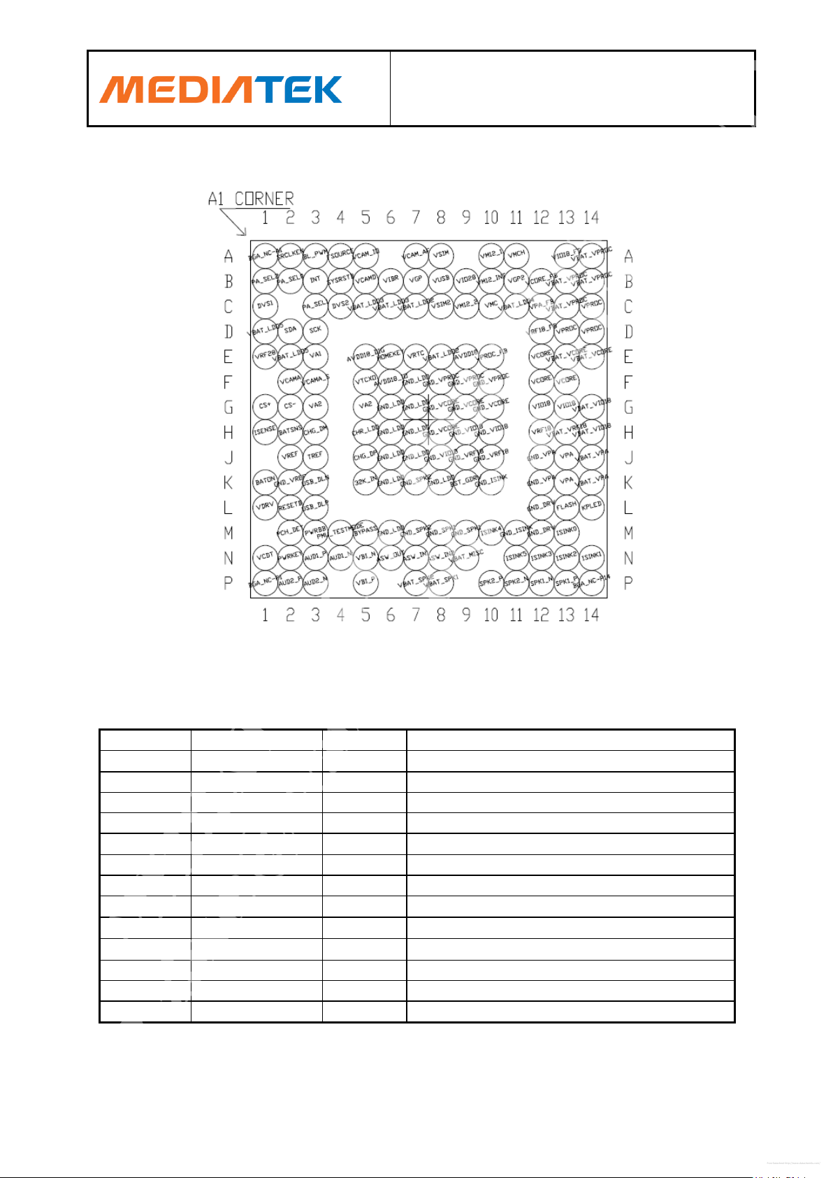
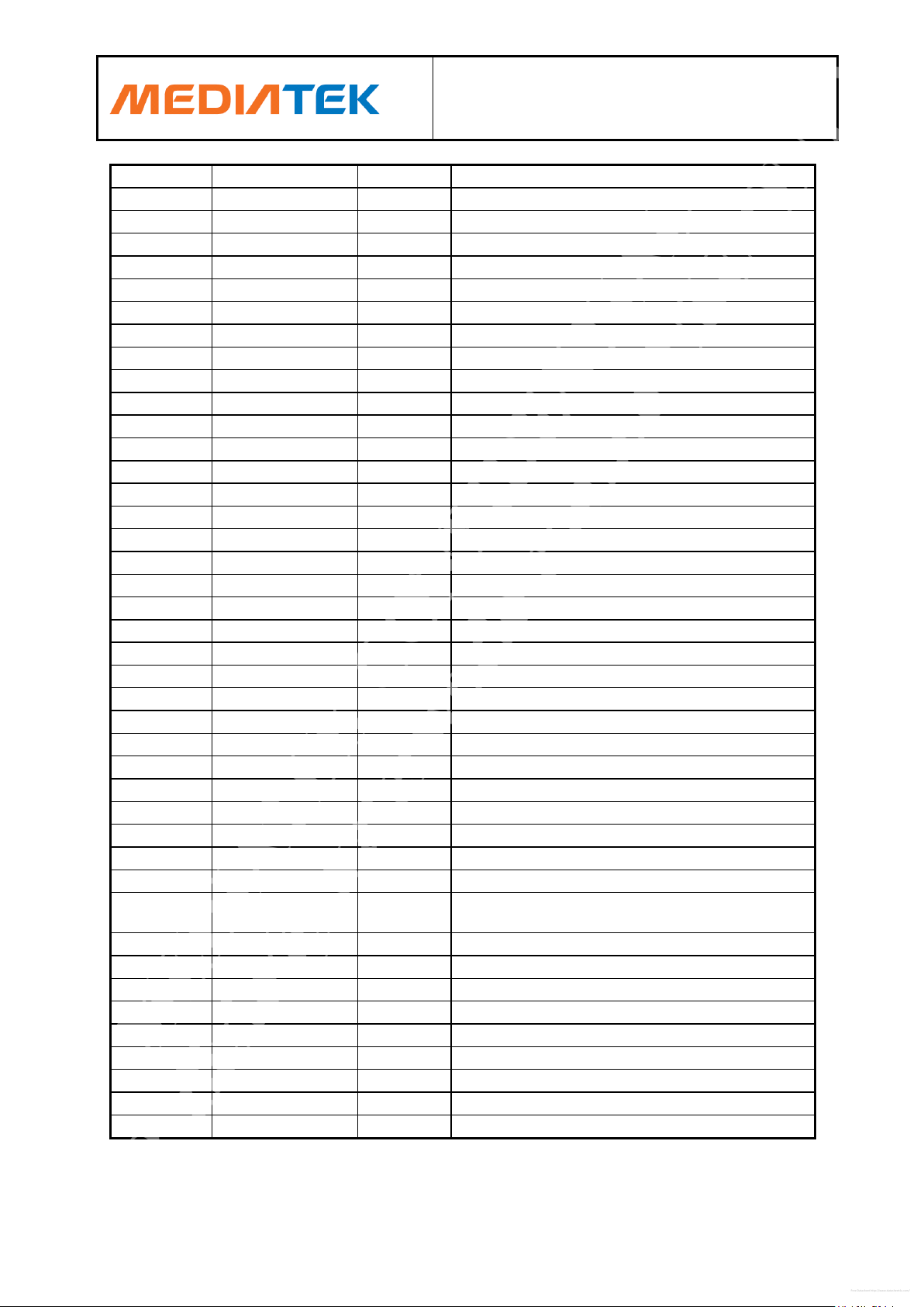
1.6 Pin Assignments and Descriptions
Figure 1: MT6329 TFBGA 155 (7.1x7.1mm) pin assignment
Table 2: MT6329 pin descriptions
MEDIATEK CONFIDENTIAL
This document contains information that is proprietary to MediaTek Inc.
Unauthorized reproduction or disclosure of this information in whole or in part is strictly prohibited.
FOR zlixin@ waterworld.com.cn USE ONLY
MT6329
PMIC Datasheet
Confidential A
MediaTek Confidential
© 2011 - 2012 MediaTek Inc.
Page 9 of 97
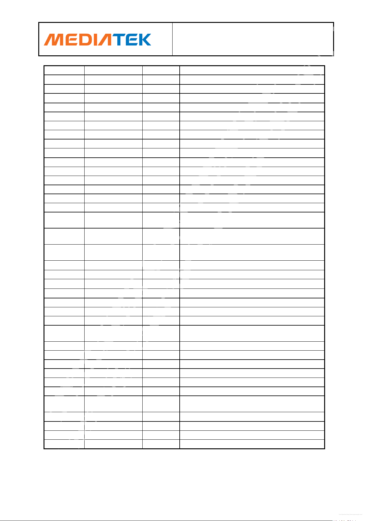
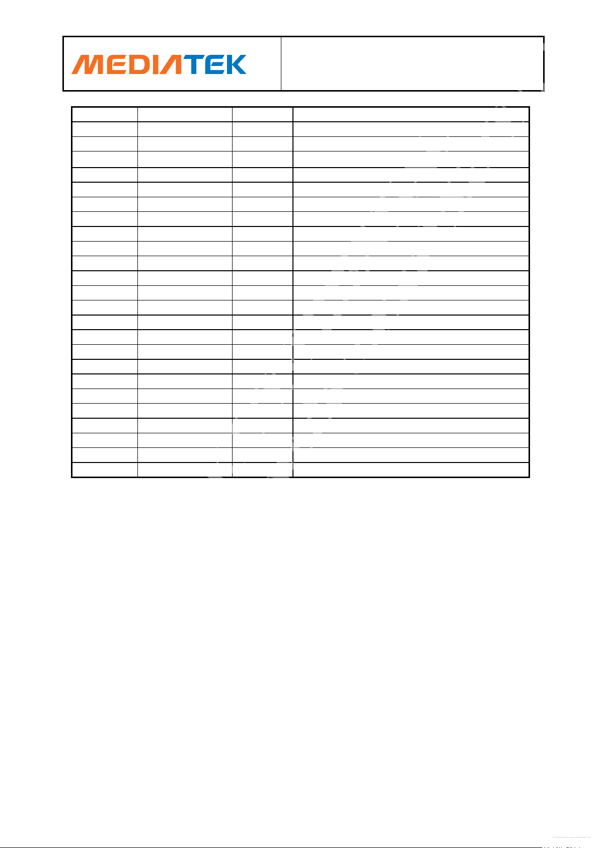
Ball
Symbol
I/O
Description
B3
INT
O
Interrupt output
B4
SYSRSTB
I
External system reset input pin (active low)
B5
VCAMD
O
LDO output used for camera digital
B6
VIBR
O
LDO output used for vibrator
B7
VGP
O
LDO output reserved for further system use
B8
VUSB
O
LDO output used for USB
B9
VIO28
O
LDO output used for 2.8V IO
B10
VM12_INT
O
LDO output used for 1.2V SRAM
B11
VGP2
O
LDO output reserved for further system use
B12
VCORE_FB
I
VCORE feedback input
B13
VBAT_VPROC
PWR
VBAT for VPROC
B14
VBAT_VPROC
PWR
VBAT for VPROC
C1
DVS1
I
VPROC output voltage selection
C3
PA_SEL1
I
PA output voltage selection
C4
DVS2
I
VPROC output voltage selection
C5
VBAT_LDO3
PWR
VBAT for VIBR, VCAM_IO, VCAMD, VRTC and
IBIAS_DLDO1
C6
VBAT_LDO3
PWR
VBAT for VIBR, VCAM_IO, VCAMD, VRTC and
IBIAS_DLDO1
C7
VBAT_LDO2
PWR
VBAT for VIO28, VSIM, VSIM2, VUSB, VGP and
VCAM_AF
C8
VSIM2
O
LDO output used for 2nd SIM card
C9
VM12_2
O
LDO output for 1.2V DRAM or AST3002
C10
VMC
O
LDO output for memory card
C11
VBAT_LDO4
PWR
VBAT for VMC, VMCH, VGP2 and IBIAS_DLDO2
C12
VPA_FB
I
VPA feedback input
C13
VBAT_VPROC
PWR
VBAT for VPROC
C14
VPROC
O
VPROC switching output
D1
VBAT_LDO5
PWR
VBAT for VA1, VA2, VCAMA, VTCXO, VRF28
and IBIAS_ALDO
D2
SDA
I
I2C serial data
D3
SCK
I
I2C serial clock
D12
VRF18_FB
I
VRF18 feedback input
D13
VPROC
O
VPROC switching output
D14
VPROC
O
VPROC switching output
E1
VRF28
O
LDO output for RF
E2
VBAT_LDO5
PWR
VBAT for VA1, VA2, VCAMA, VTCXO, VRF28
and IBIAS_ALDO
E3
VA1
O
LDO output for analog baseband
E5
AVDD18_DIG
O
LDO output bypass pin
E6
HOMEKEY
I
Homekey
E7
VRTC
O
LDO output for RTC
Free Datasheet http://www.datasheet4u.com/
MEDIATEK CONFIDENTIAL
This document contains information that is proprietary to MediaTek Inc.
Unauthorized reproduction or disclosure of this information in whole or in part is strictly prohibited.
FOR zlixin@ waterworld.com.cn USE ONLY
MT6329
PMIC Datasheet
Confidential A
MediaTek Confidential
© 2011 - 2012 MediaTek Inc.
Page 10 of 97
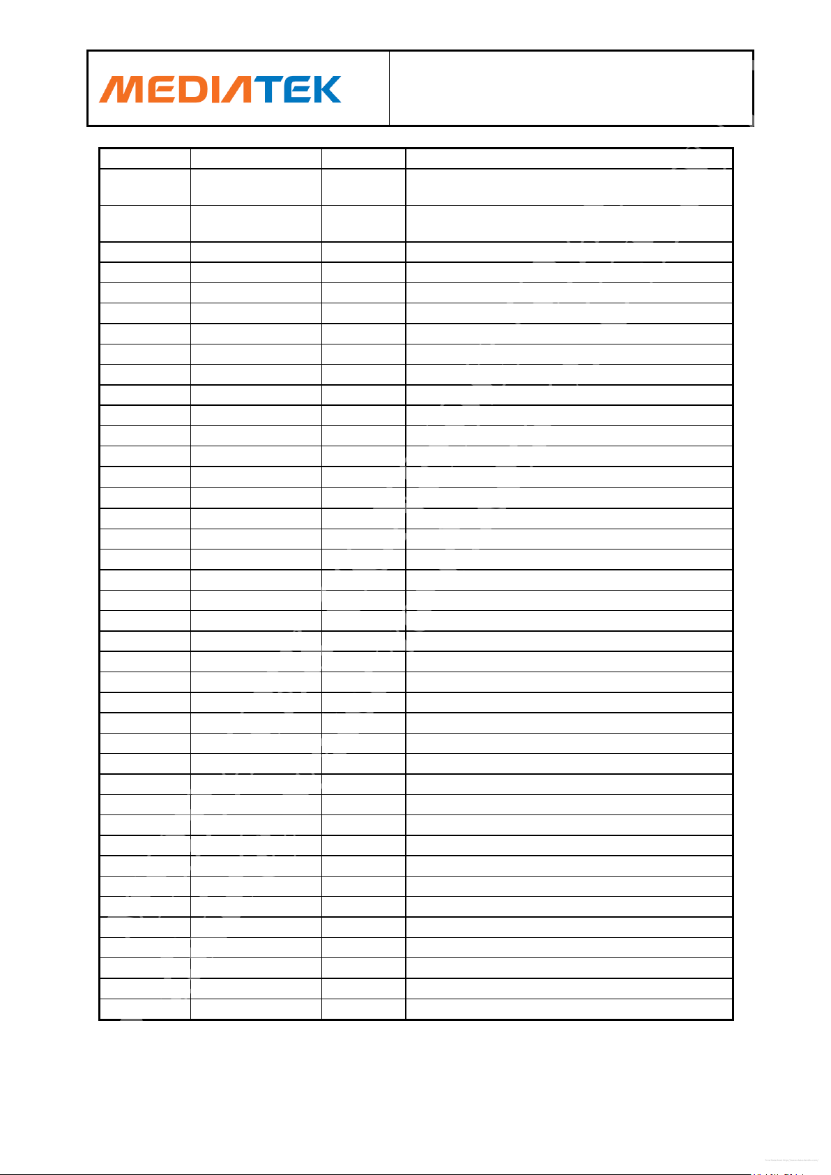
Ball
Symbol
I/O
Description
E8
VBAT_LDO2
PWR
VBAT for VIO28, VSIM, VSIM2, VUSB, VGP and
VCAM_AF
E9
AVDD18
PWR
1.8V power input for VM12_1, VM12_2 and
VM12_INT
E10
VPROC_FB
I
VPROC feedback input
E12
VCORE
O
VCORE switching output
E13
VBAT_VCORE
PWR
VBAT for VCORE
E14
VBAT_VCORE
PWR
VBAT for VCORE
F2
VCAMA
O
LDO output for camaera analog
F3
VCAMA_S
I
Sense input for VCAMA LDO
F5
VTCXO
O
LDO output for TCXO
F6
AVDD18_IO
PWR
1.8V IO power input for internal GPIO
F7
GND_LDO
GND
GND for LDO
F8
GND_VPROC
GND
GND for VPROC
F9
GND_VPROC
GND
GND for VPROC
F10
GND_VPROC
GND
GND for VPROC
F12
VCORE
O
VCORE switching output
F13
VCORE
O
VCORE switching output
G1
CS+
I
Fuel gauge positive current sense point
G2
CS-
I
Fuel gauge negative current sense point
G3
VA2
O
LDO output for analog baseband
G5
VA2_BUF
O
LDO output for analog baseband
G6
GND_LDO
GND
GND for LDO
G7
GND_LDO
GND
GND for LDO
G8
GND_VCORE
GND
GND for VCORE
G9
GND_VCORE
GND
GND for VCORE
G10
GND_VCORE
GND
GND for VCORE
G12
VIO18
O
VIO18 switching output
G13
VIO18
O
VIO18 switching output
G14
VBAT_VIO18
PWR
VBAT for VIO18
H1
ISENSE
I
Charging current sense input
H2
BATSNS
I
Battery voltage sense input
H3
CHG_DM
I
USB D- for BC1.1 standard
H5
CHR_LDO
O
Charger LDO output bypass pin
H6
GND_LDO
GND
GND for LDO
H7
GND_LDO
GND
GND for LDO
H8
GND_VCORE
GND
GND for VCORE
H9
GND_VIO18
GND
GND for VIO18
H10
GND_VIO18
GND
GND for VIO18
H12
VRF18
O
VRF18 switching output
H13
VBAT_VRF18
PWR
VBAT for VRF18
H14
VBAT_VIO18
PWR
VBAT for VIO18
Free Datasheet http://www.datasheet4u.com/
MEDIATEK CONFIDENTIAL
This document contains information that is proprietary to MediaTek Inc.
Unauthorized reproduction or disclosure of this information in whole or in part is strictly prohibited.
FOR zlixin@ waterworld.com.cn USE ONLY
MT6329
PMIC Datasheet
Confidential A
MediaTek Confidential
© 2011 - 2012 MediaTek Inc.
Page 11 of 97
Ball
Symbol
I/O
Description
J2
VREF
O
Internal reference bypass
J3
TREF
O
Battery thermal detection reference voltage
J5
CHG_DP
I
USB D+ for BC1.1 standard
J6
GND_LDO
GND
GND for LDO
J7
GND_LDO
GND
GND for LDO
J8
GND_VIO18
GND
GND for VIO18
J9
GND_VRF18
GND
GND for VRF18
J10
GND_VRF18
GND
GND for VRF18
J12
GND_VPA
GND
GND for VPA
J13
VPA
O
VPA switching output
J14
VBAT_VPA
PWR
VBAT for VPA
K1
BATON
I
Battery thermal detection input
K2
GND_VREF
GND
GND for reference
K3
USB_DLN
I
USB download key
K5
32K_IN
I
RTC 32K input used for fuel gauge operation
K6
GND_LDO
GND
GND for LDO
K7
GND_SPK2
GND
GND for speaker channel 2
K8
GND_LDO
GND
GND for LDO
K9
BST_GDRV
O
Boost controller gate drvie output
K10
GND_ISINK
GND
GND for ISINK
K12
GND_VPA
GND
GND for VPA
K13
VPA
O
VPA switching output
K14
VBAT_VPA
PWR
VBAT for VPA
L1
VDRV
O
Charger current drive output
L2
RESETB
O
Reset output
L3
USB_DLP
I
USB download key
L12
GND_DRV
GND
GND for flashligh and keypad LDO drivers
L13
FLASH
O
Flashlight open drain output
L14
KPLED
O
Keypad LED open drain output
M2
PCH_DET
O
Charging indicator current sink output
M3
PWRBB
I
Power on RTC domain latch signal
M4
PMU_TESTMODE
I
Test mode input (normal function should tie to
GND)
M5
BYPASS
O
SPK common mode voltage bypass
M6
GND_LDO
GND
GND for LDO
M7
GND_SPK2
GND
GND for speaker channel 2
M8
GND_SPK1
GND
GND for speaker channel 1
M9
GND_SPK1
GND
GND for speaker channel 1
M10
ISINK4
O
Current sink channel 4 output
M11
GND_ISINK
GND
GND for ISINK
M12
GND_DRV
GND
GND for flashligh and keypad LDO drivers
M13
ISINK0
O
Current sink channel 0 output
Free Datasheet http://www.datasheet4u.com/
MEDIATEK CONFIDENTIAL
This document contains information that is proprietary to MediaTek Inc.
Unauthorized reproduction or disclosure of this information in whole or in part is strictly prohibited.
FOR zlixin@ waterworld.com.cn USE ONLY
MT6329
PMIC Datasheet
Confidential A
MediaTek Confidential
© 2011 - 2012 MediaTek Inc.
Page 12 of 97
Ball
Symbol
I/O
Description
N1
VCDT
I
Ratioed charger input voltage
N2
PWRKEY
I
Power key
N3
AUD1_P
I
Audio channel 1 differential input (positive)
N4
AUD1_N
I
Audio channel 1 differential input (negative)
N5
VBI_N
I
Voice differential input (negative)
N6
ASW_OUT
O
Analog switch output
N7
ASW_IN1
I
Analog switch input 1
N8
ASW_IN2
I
Analog switch input 2
N9
VBAT_MISC
PWR
VBAT for buck, driver and speaker controller
N11
ISINK5
O
Current sink channel 5 output
N12
ISINK3
O
Current sink channel 4 output
N13
ISINK2
O
Current sink channel 3 output
N14
ISINK1
O
Current sink channel 1 output
P1
BGA_NC-P1
I/O
NC
P2
AUD2_P
I
Audio channel 2 differential input (positive)
P3
AUD2_N
I
Audio channel 2 differential input (negative)
P5
VBI_P
I
Voice differential input (positive)
P7
VBAT_SPK2
PWR
VBAT for speaker channel 2
P8
VBAT_SPK1
PWR
VBAT for speaker channel 1
P10
SPK2_P
O
Speaker channel 2 differential output (positive)
P11
SPK2_N
O
Speaker channel 2 differential output (negative)
P12
SPK1_N
O
Speaker channel 1 differential output (negative)
P13
SPK1_P
O
Speaker channel 1 differential output (positive)
P14
BGA_NC-P14
I/O
NC
Free Datasheet http://www.datasheet4u.com/
MEDIATEK CONFIDENTIAL
This document contains information that is proprietary to MediaTek Inc.
Unauthorized reproduction or disclosure of this information in whole or in part is strictly prohibited.
FOR zlixin@ waterworld.com.cn USE ONLY

MT6329
PMIC Datasheet
Confidential A
MediaTek Confidential
© 2011 - 2012 MediaTek Inc.
Page 13 of 97
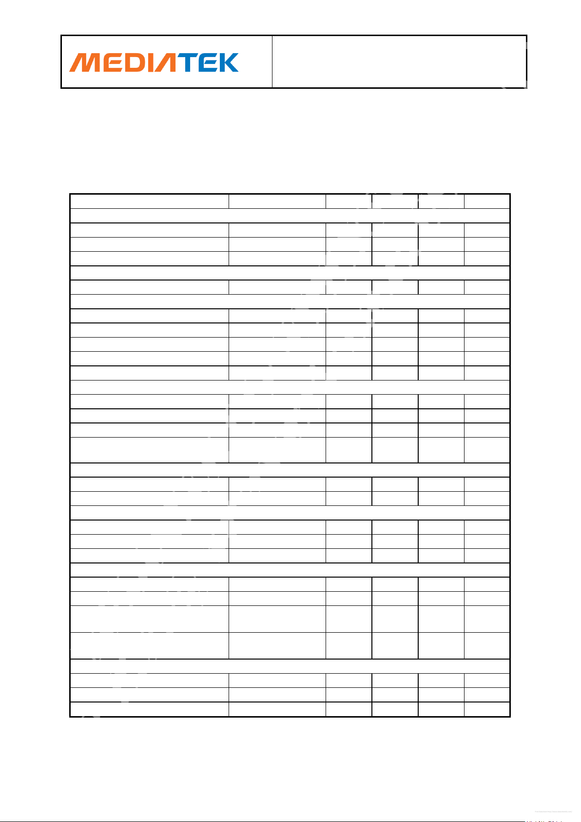
Parameter
Conditions
Min.
Typical
Max.
Unit
Free-air temperature range
-40 85
°C
Storage temperature range
-65 150
°C
Battery input voltage range
4.3
V
ESD robustness
HBM
2,000
V
Charger input withstand
10
V
Parameter
Conditions
Min.
Typical
Max.
Unit
Thermal resistance from
junction to ambient
In free air
39.8[1]
°C/W
Parameter
Conditions
Min.
Typical
Max.
Unit
Operating temperature range
-25 85
°C
Free Datasheet http://www.datasheet4u.com/
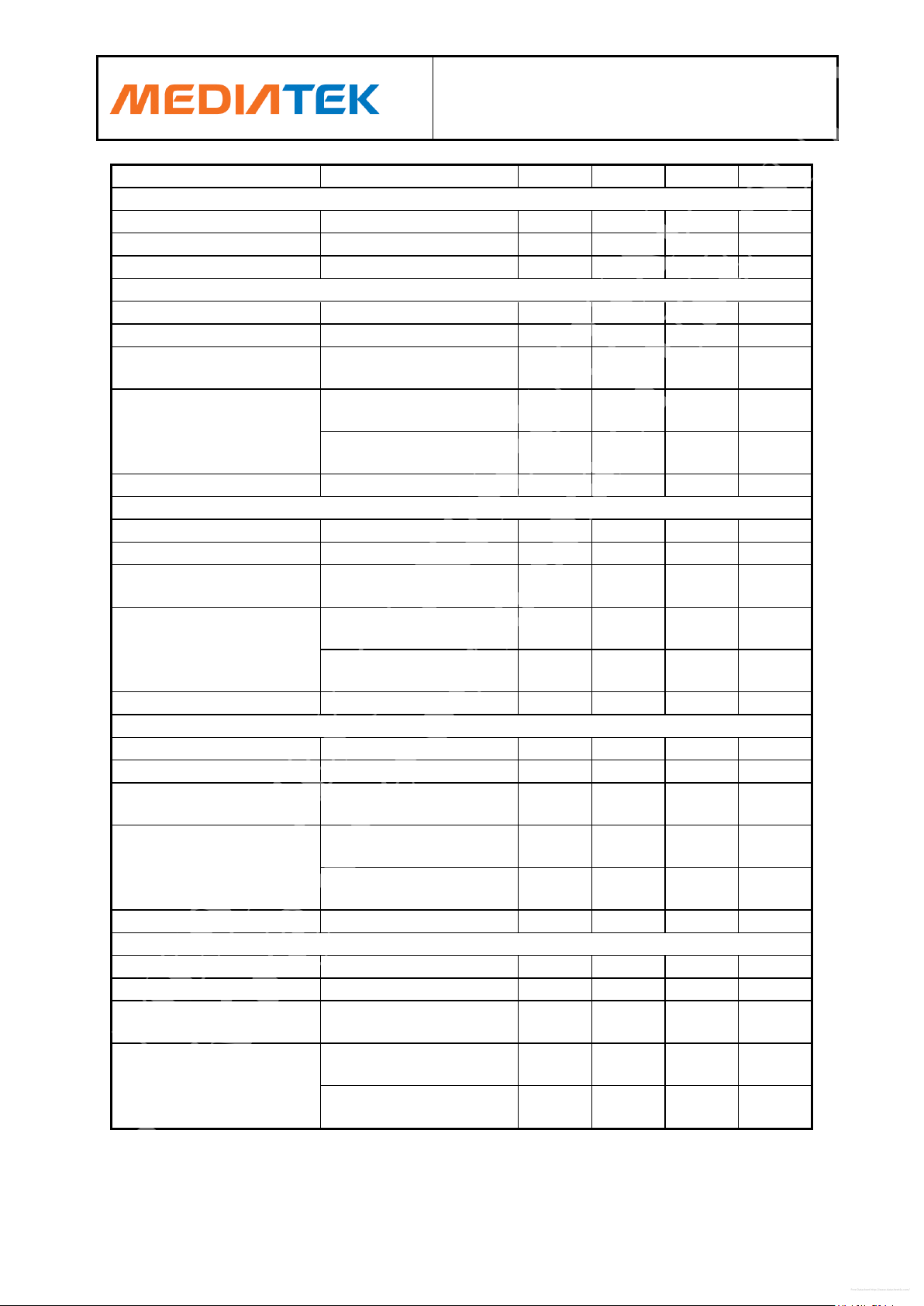
2 Electrical Characteristics
2.1 Absolute Maximum Ratings over Operating Free-Air Temperature Range
Stresses beyond those listed under Table 3 may cause permanent damage to the device. These
numbers are stress ratings only, and functional operation of the device at these or any other
conditions beyond those indicated in the operational sections of specifications is not implied.
Exposure to absolute maximum rating conditions for extended periods may affect the device reliability.
Table 3: Absolute maximum ratings
2.2 Thermal Characteristic
Note: The device is mounted on a 4-metal-layer PCB and modeled per JEDEC51-9 condition.
2.3 Pin Voltage Rating (TBD)
2.4 Recommended Operating Range
MEDIATEK CONFIDENTIAL
Table 4: Operation condition
FOR zlixin@ waterworld.com.cn USE ONLY
This document contains information that is proprietary to MediaTek Inc.
Unauthorized reproduction or disclosure of this information in whole or in part is strictly prohibited.
MT6329
PMIC Datasheet
Confidential A
MediaTek Confidential
© 2011 - 2012 MediaTek Inc.
Page 14 of 97
Parameter
Conditions
Min.
Typical
Max.
Unit
Switch-off mode: supply current
VBAT < 2.4 V
RTC LDO OFF
85 μA
2.4 V < VBAT < 3.2 V
35 μA
3.2 V < VBAT
60 μA
Operation ground current
Standby
Low-power mode
300 μA
Under voltage (UV)
Under voltage falling threshold 1
UV_SEL[1:0] = 00
2.8
2.9
3.0
V
Under voltage falling threshold 2
UV_SEL[1:0] = 01
2.75 V
Under voltage falling threshold 3
UV_SEL[1:0] = 10
2.6 V
Under voltage falling threshold 4
UV_SEL[1:0] = 11
2.5 V
Under voltage rising threshold
UV_SEL[1:0] = xx
3.1
3.2
3.3
V
Reset generator
Output high
VIO-0.4
V
Output low
0.2
V
Output current (Ioh)
Vo > VIO-0.4V
1
mA
Delay Time from switched-on to
RESETB release
100
200
400
ms
Interrupt
Output high
VIO-0.4
V
Output low
0.2
V
Power key input
High voltage
0.7*VBAT
V
Low voltage
0.3*VBAT
V
De-bounce time
25
50
200
Control input voltage
PWRBB input high
2.1
V
PWRBB input low
0.54
V
Other control input high
(SRCLKEN, PA_SEL)
2.0
V
Other control input low
(SRCLKEN, PA_SEL)
0.5
V
Thermal shut-down
PMIC shut-down threshold
150
degree
SW high power latch threshold
125
degree
Interrupt threshold
110
degree
Free Datasheet http://www.datasheet4u.com/
2.5 Electrical Characteristics
VBAT = 3.4 ~ 4.2V, minimum loads applied on all outputs, unless otherwise noted.
Typical values are at TA = 25°C.
Table 5: General electrical specifications
MEDIATEK CONFIDENTIAL
FOR zlixin@ waterworld.com.cn USE ONLY
This document contains information that is proprietary to MediaTek Inc.
Unauthorized reproduction or disclosure of this information in whole or in part is strictly prohibited.
MT6329
PMIC Datasheet
Confidential A
MediaTek Confidential
© 2011 - 2012 MediaTek Inc.
Page 15 of 97
Parameter
Conditions
Min.
Typical
Max.
Unit
LDO enable response time
250 μs
Parameter
Conditions
Min.
Typical
Max.
Unit
Boost controller
Efficiency
Vin = 3.8V, 20mA, Vout =
35V
80 %
Switch on max. duty cycle
93 %
Regulated feedback voltage
(int.)
0.28
0.3
0.32
V
Turn-on rise time
1 ms
OVP on threshold
1.1
1.2
1.3
V
OVP off threshold
1 V
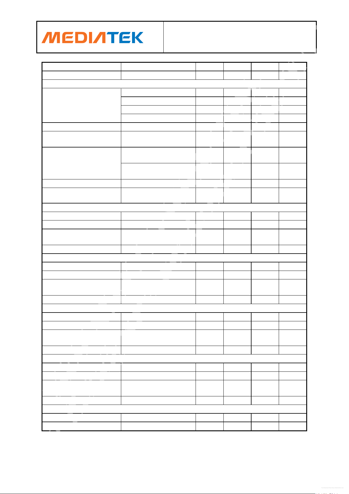
Buck - VCORE
Output voltage
1.1 V
Output current
1,000
mA
Turn-on overshoot
10
%
Load regulation
-10 10
%
Buck - VPROC
Output voltage
1.25 V
Output current
1,500
mA
Turn-on overshoot
10
%
Load regulation
-6 6
%
Buck - VIO18
Output voltage
1.8 V
Output current
1,000
mA
Turn-on overshoot
10
%
Buck - VRF18
Output voltage
1.825 V
Output current
250 mA
Turn-on overshoot
10
%
Free Datasheet http://www.datasheet4u.com/
2.6 Regulator Output
Table 6: Regulator specifications
MEDIATEK CONFIDENTIAL
FOR zlixin@ waterworld.com.cn USE ONLY
This document contains information that is proprietary to MediaTek Inc.
Unauthorized reproduction or disclosure of this information in whole or in part is strictly prohibited.
MT6329
PMIC Datasheet
Confidential A
MediaTek Confidential
© 2011 - 2012 MediaTek Inc.
Page 16 of 97
Parameter
Conditions
Min.
Typical
Max.
Unit
Buck - VPA
Output voltage
0.9 3.4
V
Output current
VOUT=3.4V
800 mA
Turn-on overshoot
10
%
ALDO - VRF28
Output voltage
2.7
2.85 3 V
Output current
200 mA
Output noise
Freq = 10 Hz to 80 kHz
Iout = 0.01Imax ~ full load
90
uVrms
PSRR
100 Hz < freq < 3 kHz
Iout = 0.01Imax/0.5Imax
65 dB
3 kHz < freq < 30 kHz
Iout = 0.01Imax/0.5Imax
45
Turn-on rise time
No load
240
us
ALDO - VTCXO
Output voltage
2.7
2.8
2.9
V
Output current
40 mA
Output noise
Freq = 10 Hz to 80 kHz
Iout = 0.01Imax ~ full load
90
uVrms
PSRR
100 Hz < freq < 3 kHz
Iout = 0.01Imax/0.5Imax
65 dB
3 kHz < freq < 30 kHz
Iout = 0.01Imax/0.5Imax
45
Turn-on rise time
No load
240
us
ALDO - VA1
Output voltage
2.35
2.5
2.65
V
Output current
100 mA
Output noise
Freq = 10 Hz to 80 kHz
Iout = 0.01Imax ~ full load
90
uVrms
PSRR
100 Hz < freq < 3 kHz
Iout = 0.01Imax/0.5Imax
65 dB
3 kHz < freq < 30 kHz
Iout = 0.01Imax/0.5Imax
45
Turn-on rise time
No load
360
us
ALDO - VA2
Output voltage
2.35
2.5
2.65
V
Output current
100 mA
Output Noise
Freq = 10 Hz to 80 kHz
Iout = 0.01Imax ~ full load
90
uVrms
PSRR
100 Hz < freq < 3 kHz
Iout = 0.01Imax/0.5Imax
65 dB
3 kHz < freq < 30 kHz
Iout = 0.01Imax/0.5Imax
45
Free Datasheet http://www.datasheet4u.com/
MEDIATEK CONFIDENTIAL
FOR zlixin@ waterworld.com.cn USE ONLY
This document contains information that is proprietary to MediaTek Inc.
Unauthorized reproduction or disclosure of this information in whole or in part is strictly prohibited.
MT6329
PMIC Datasheet
Confidential A
MediaTek Confidential
© 2011 - 2012 MediaTek Inc.
Page 17 of 97
Parameter
Conditions
Min.
Typical
Max.
Unit
Turn-on rise time
No load
360
us
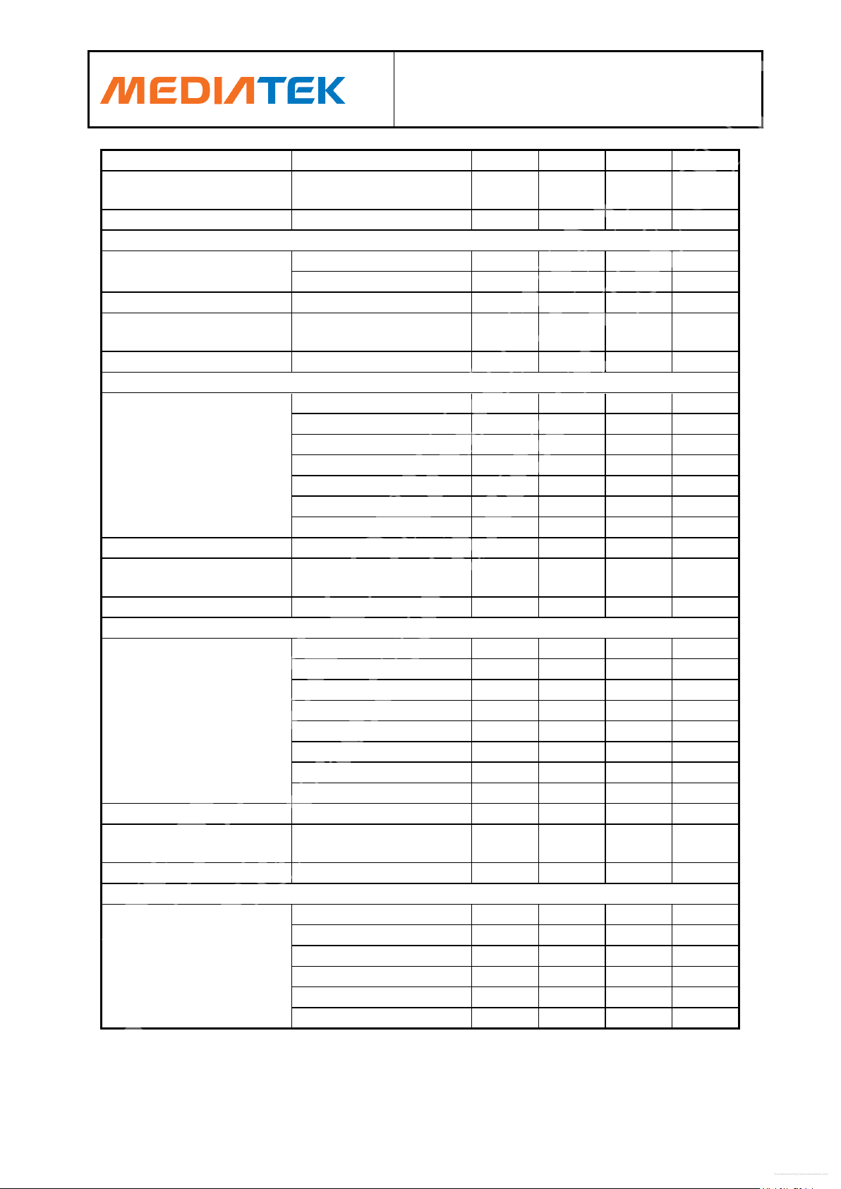
ALDO - VCAMA
Output voltage
VCAMA_SEL = 00
1.4
1.5
1.6
V
VCAMA _SEL = 01
1.7
1.8
1.9
V
VCAMA _SEL = 10
2.35
2.5
2.65
V
VCAMA _SEL = 11
2.65
2.8
2.95
V
Output current
200 mA
Output noise
Freq = 10 Hz to 80 kHz
Iout = 0.01Imax ~ full load
40
uVrms
PSRR
100 Hz < freq < 3 kHz
Iout = 0.01Imax/0.5Imax
65 dB
3 kHz < freq < 30 kHz
Iout = 0.01Imax/0.5Imax
45
Turn-on rise time
No load
1,000
us
Load transient response
IOUT = 1mA to full Load
(15mA/usec)
40
mV
DLDO - VM12_1
Output voltage
1.1
1.2
1.3
V
Output current
300 mA
PSRR
Freq = 217 Hz
Iout = 0.01Imax/0.5Imax
40 dB
Turn-on rise time
No load
360
us
DLDO - VM12_2
Output voltage
1.1
1.2
1.3
V
Output current
300 mA
PSRR
Freq = 217 Hz
Iout = 0.01Imax/0.5Imax
40 dB
Turn-on rise time
No load
360
us
DLDO - VM12_INT
Output voltage
1.1
1.2
1.3
V
Output current
360 mA
PSRR
Freq = 217 Hz
Iout = 0.01Imax/0.5Imax
40 dB
Turn-on rise Time
No load
360
us
DLDO - VIO28
Output voltage
2.65
2.8
2.95
V
Output current
100 mA
PSRR
Freq = 217 Hz
Iout = 0.01Imax/0.5Imax
40 dB
Turn-on rise time
No load
360
us
DLDO - USB
Output voltage
3.1
3.3
3.5
V
Output current
100 mA
Free Datasheet http://www.datasheet4u.com/
MEDIATEK CONFIDENTIAL
FOR zlixin@ waterworld.com.cn USE ONLY
This document contains information that is proprietary to MediaTek Inc.
Unauthorized reproduction or disclosure of this information in whole or in part is strictly prohibited.
MT6329
PMIC Datasheet
Confidential A
MediaTek Confidential
© 2011 - 2012 MediaTek Inc.
Page 18 of 97
Parameter
Conditions
Min.
Typical
Max.
Unit
PSRR
Freq = 217 Hz
Iout = 0.01Imax/0.5Imax
40 dB
Turn-on rise time
No load
360
us
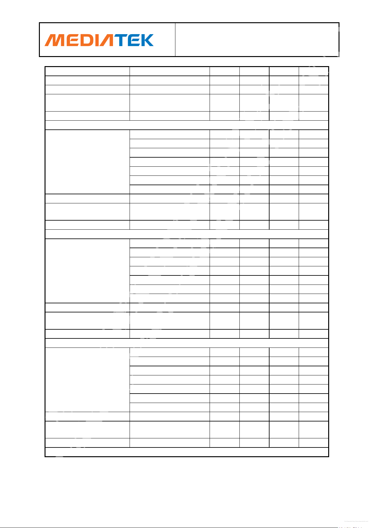
DLDO - SIM1
Output voltage
VSIM1_SEL = 0
1.7
1.8
1.9
V
VSIM1_SEL = 1
2.85
3.0
3.15
V
Output current
100 mA
PSRR
Freq = 217 Hz
Iout = 0.01Imax/0.5Imax
40 dB
Turn-on rise time
No load
360
us
DLDO - SIM2
Output voltage
VSIM2_SEL = 000
1.2
1.3
1.4
V
VSIM2_SEL = 001
1.4
1.5
1.6
V
VSIM2_SEL = 010
1.7
1.8
1.9
V
VSIM2_SEL = 011
2.35
2.5
2.65
V
VSIM2_SEL = 100
2.65
2.8
2.95
V
VSIM2_SEL = 101
2.85
3.0
3.15
V
VSIM2_SEL = 110
3.1
3.3
3.5
V
Output current
100 mA
PSRR
Freq = 217 Hz
Iout = 0.01Imax/0.5Imax
40 dB
Turn-on rise time
No load
360
us
DLDO - VCAMD
Output voltage
VCAMD_SEL = 000
1.2
1.3
1.4
V
VCAMD_SEL = 001
1.4
1.5
1.6
V
VCAMD_SEL = 010
1.7
1.8
1.9
V
VCAMD_SEL = 011
2.35
2.5
2.65
V
VCAMD_SEL = 100
2.65
2.8
2.95
V
VCAMD_SEL = 101
2.85
3.0
3.15
V
VCAMD_SEL = 110
3.1
3.3
3.5
V
VCAMD_SEL = 1111
1.1
1.2
1.3
Output current
300 mA
PSRR
Freq = 217 Hz
Iout = 0.01Imax/0.5Imax
40 dB
Turn-on rise time
No load
360
us
DLDO - VCAM_IO
Output voltage
VCAM_IO_SEL = 000
1.2
1.3
1.4
V
VCAM_IO_SEL = 001
1.4
1.5
1.6
V
VCAM_IO_SEL = 010
1.7
1.8
1.9
V
VCAM_IO_SEL = 011
2.35
2.5
2.65
V
VCAM_IO_SEL = 100
2.65
2.8
2.95
V
VCAM_IO_SEL = 101
2.85
3.0
3.15
V
Free Datasheet http://www.datasheet4u.com/
MEDIATEK CONFIDENTIAL
FOR zlixin@ waterworld.com.cn USE ONLY
This document contains information that is proprietary to MediaTek Inc.
Unauthorized reproduction or disclosure of this information in whole or in part is strictly prohibited.
MT6329
PMIC Datasheet
Confidential A
MediaTek Confidential
© 2011 - 2012 MediaTek Inc.
Page 19 of 97
Parameter
Conditions
Min.
Typical
Max.
Unit
VCAM_IO_SEL = 110
3.1
3.3
3.5
V
Output current
100 mA
PSRR
Freq = 217 Hz
Iout = 0.01Imax/0.5Imax
40 dB
Turn-on rise time
No load
360
us
DLDO - VCAM_AF
Output voltage
VCAM_AF_SEL = 000
1.2
1.3
1.4
V
VCAM_AF_SEL = 001
1.4
1.5
1.6
V
VCAM_AF_SEL = 010
1.7
1.8
1.9
V
VCAM_AF_SEL = 011
2.35
2.5
2.65
V
VCAM_AF_SEL = 100
2.65
2.8
2.95
V
VCAM_AF_SEL = 101
2.85
3.0
3.15
V
VCAM_AF_SEL = 110
3.1
3.3
3.5
V
Output current
200 mA
PSRR
Freq = 217 Hz
Iout = 0.01Imax/0.5Imax
40 dB
Turn-on rise time
No load
360
us
DLDO - VMC
Output voltage
VMC_SEL = 000
1.2
1.3
1.4
V
VMC_SEL = 001
1.4
1.5
1.6
V
VMC_SEL = 010
1.7
1.8
1.9
V
VMC_SEL = 011
2.35
2.5
2.65
V
VMC_SEL = 100
2.65
2.8
2.95
V
VMC_SEL = 101
2.85
3.0
3.15
V
VMC_SEL = 110
3.1
3.3
3.5
V
Output current
200 mA
PSRR
Freq = 217 Hz
Iout = 0.01Imax/0.5Imax
40 dB
Turn-on rise time
No load
40
us
DLDO - VMCH
Output voltage
VMCH_SEL = 000
1.2
1.3
1.4
V
VMCH_SEL = 001
1.4
1.5
1.6
V
VMCH_SEL = 010
1.7
1.8
1.9
V
VMCH_SEL = 011
2.35
2.5
2.65
V
VMCH_SEL = 100
2.65
2.8
2.95
V
VMCH_SEL = 101
2.85
3.0
3.15
V
VMCH_SEL = 110
3.1
3.3
3.5
V
Output current
400 mA
PSRR
Freq = 217 Hz
Iout = 0.01Imax/0.5Imax
40 dB
Turn-on rise time
No load
40
us
DLDO - VGP1
Free Datasheet http://www.datasheet4u.com/
MEDIATEK CONFIDENTIAL
FOR zlixin@ waterworld.com.cn USE ONLY
This document contains information that is proprietary to MediaTek Inc.
Unauthorized reproduction or disclosure of this information in whole or in part is strictly prohibited.
MT6329
PMIC Datasheet
Confidential A
MediaTek Confidential
© 2011 - 2012 MediaTek Inc.
Page 20 of 97
Parameter
Conditions
Min.
Typical
Max.
Unit
Output voltage
VGP1_SEL = 000
1.2
1.3
1.4
V
VGP1_SEL = 001
1.4
1.5
1.6
V
VGP1_SEL = 010
1.7
1.8
1.9
V
VGP1_SEL = 011
2.35
2.5
2.65
V
VGP1_SEL = 100
2.65
2.8
2.95
V
VGP1_SEL = 101
2.85
3.0
3.15
V
VGP1_SEL = 110
3.1
3.3
3.5
V
Output current
200 mA
PSRR
Freq = 217 Hz
Iout = 0.01Imax/0.5Imax
40 dB
Turn-on rise time
No load
360
us
DLDO - VGP2
Output voltage
VGP2_SEL = 000
1.2
1.3
1.4
V
VGP2_SEL = 001
1.4
1.5
1.6
V
VGP2_SEL = 010
1.7
1.8
1.9
V
VGP2_SEL = 011
2.35
2.5
2.65
V
VGP2_SEL = 100
2.65
2.8
2.95
V
VGP2_SEL = 101
2.85
3.0
3.15
V
VGP2_SEL = 110
3.1
3.3
3.5
V
Output current
100 mA
PSRR
Freq = 217 Hz
Iout = 0.01Imax/0.5Imax
40 dB
Turn-on rise time
No load
360
us
DLDO - VIBR
Output voltage
VIBR_SEL = 000
1.2
1.3
1.4
V
VIBR_SEL = 001
1.4
1.5
1.6
V
VIBR_SEL = 010
1.7
1.8
1.9
V
VIBR_SEL = 011
2.35
2.5
2.65
V
VIBR_SEL = 100
2.65
2.8
2.95
V
VIBR_SEL = 101
2.85
3.0
3.15
V
VIBR_SEL = 110
3.1
3.3
3.5
V
Output current
100 mA
PSRR
Freq = 217 Hz
Iout = 0.01Imax/0.5Imax
40 dB
Turn-on rise time
No load
360
us
Class AB parameter
Conditions
Min.
Typical
Max.
Unit
Free Datasheet http://www.datasheet4u.com/
2.7 Class AB/D Audio Amplifier
FOR zlixin@ waterworld.com.cn USE ONLY
MEDIATEK CONFIDENTIAL
Table 7: Class AB/D audio amplifier specifications
This document contains information that is proprietary to MediaTek Inc.
Unauthorized reproduction or disclosure of this information in whole or in part is strictly prohibited.
MT6329
PMIC Datasheet
Confidential A
MediaTek Confidential
© 2011 - 2012 MediaTek Inc.
Page 21 of 97
Class AB parameter
Conditions
Min.
Typical
Max.
Unit
RMS power
8Ω load, VBAT = 4.2 V
THD + N = 1%
850
mW
8Ω load, VBAT = 3.7 V
THD + N = 1%
700
mW
8Ω load, VBAT = 3.4 V
THD + N = 1%
600
mW
THD+N
1 kHz, Po = 0.5Wrms, 4.2V
0.05
0.2
%
PSRR
217 Hz, Vin = 200mVpk-pk
Input AC to ground
75
85 dB
1 kHz, Vin = 200mVpk-pk
Input AC to ground
75
85 dB
4 kHz, Vin = 200mVpk-pk
Input AC to ground
75
85 dB
20 kHz, Vin = 200mVpk-pk
Input AC to ground
50 dB
Noise level
VBAT = 3.3V 0dB gain
8Ω, A-weighted
25
70
μV
VBAT = 4.2V 0dB Gain
8Ω, A-weighted
25
70
uV
Gain adjustment
3
21
dB
Gain adjustment steps
3 dB
Quiescent current
No load 3 6 mA
CMRR
VBAT=3.4/3.8/4.2V
f=1kHz, Vin=200mVpk-pk
49
60 Ω
Class D parameter
Conditions
Min.
Typical
Max.
Unit
RMS power
8Ω load, VBAT = 4.2 V
THD + N = 1%
900
mW
8Ω load, VBAT = 3.7 V
THD + N = 1%
700
mW
8Ω load, VBAT = 3.4V
THD + N = 1%
600
mW
THD+N
1 kHz, Po = 0.5Wrms, 4.2V
0.2
%
PSRR
217 Hz, Vin = 200mVpk-pk
Input AC to ground
65
75 dB
1 kHz, Vin = 200mVpk-pk
Input AC to ground
65
75 dB
4 kHz, Vin = 200mVpk-pk
Input AC to ground
65
75 dB
20 kHz, Vin = 200mVpk-pk
Input AC to ground
50 dB
Noise level
VBAT = 3.3V 0dB gain
8Ω, A-weighted
25
70
μV
VBAT = 4.2V 0dB gain
25
70
uV
Free Datasheet http://www.datasheet4u.com/
MEDIATEK CONFIDENTIAL
FOR zlixin@ waterworld.com.cn USE ONLY
This document contains information that is proprietary to MediaTek Inc.
Unauthorized reproduction or disclosure of this information in whole or in part is strictly prohibited.
MT6329
PMIC Datasheet
Confidential A
MediaTek Confidential
© 2011 - 2012 MediaTek Inc.
Page 22 of 97
Class D parameter
Conditions
Min.
Typical
Max.
Unit
8Ω, A-weighted
Efficiency
VBAT = 4.2V
0.8W, 8Ω with 68uH, 1 kHz
80
90 %
Gain adjustment
Mute 21
dB
Gain adjustment steps
3 dB
Quiescent current
No load 4 6 mA
CMRR
VBAT = 3.4/3.8/4.2V
f=1 kHz, Vin = 200mVpk-pk
49
60 Ω
Parameter
Conditions
Min.
Typical
Max.
Unit
CHRIN voltage
4.3 5 7
V
Operation range VCGRIN
3.2 5 8
V
OTG detection
0.8
2.4 4 V
VCDT CHRIN detection
threshold
VCDT_VTHL[3:0] = 0000 ~
1111
4.2
10.5
V
HV adaptive current @
pre_charge
VCDT switch threshold
(200mA => 70mA)
6
V
Pre-charging indicator
Vchg = 3.3/5V
4.5mA VISINK drop
1000
mV
VBAT CC
3.15
3.3
3.45
V
VBAT CV
4.15
4.2
4.25
V
VBAT OV
4.25
4.3
4.35
V
CC mode charging current
CS_VTH = 1111
14/R
sense
mA
CS_VTH = 1110
40/R
sense
mA
CS_VTH = 1101
80/R
sense
mA
CS_VTH = 1100
90/R
sense
mA
CS_VTH = 1011
110/R
sense
mA
CS_VTH = 1010
130/R
sense
mA
CS_VTH = 1001
140/R
sense
mA
CS_VTH = 1000
160/R
sense
mA
CS_VTH = 0111
180/R
sense
mA
CS_VTH = 0110
200/R
sense
mA
CS_VTH = 0101
220/R
sense
mA
CS_VTH = 0100
240/R
sense
mA
CS_VTH = 0011
260/R
sense
mA
CS_VTH = 0010
280/R
sense
mA
CS_VTH = 0001
300/R
sense
mA
Free Datasheet http://www.datasheet4u.com/
2.8 Battery Charger
Table 8: Charger specifications
MEDIATEK CONFIDENTIAL
FOR zlixin@ waterworld.com.cn USE ONLY
This document contains information that is proprietary to MediaTek Inc.
Unauthorized reproduction or disclosure of this information in whole or in part is strictly prohibited.
MT6329
PMIC Datasheet
Confidential A
MediaTek Confidential
© 2011 - 2012 MediaTek Inc.
Page 23 of 97
Parameter
Conditions
Min.
Typical
Max.
Unit
CS_VTH = 0000
320/R
sense
mA
UVLO
VTHH 3.2 V
VTHL 2.9 V
DDLO
VTHH 2.7 V
VTHL 2.5 V
Parameter
Conditions
Min.
Typical
Max.
Unit
Flash dropout voltage
VFlash @ ISINK = 450mA
0.5
V
Flash soft start time
VFlash @ ISINK = 300mA
1
ms
KPLED dropout voltage
KPLED @ ISINK = 150mA
0.5
V
KPLED soft start time
KPLED @ ISINK = 150mA
1
ms
ISINK current matching
VISINK = 0.3 ~ 2.5V
4/24mA, 5 LEDs
-5 5
%
ISINK LED sink current
ISINK_SEL = 000
4
mA
ISINK_SEL = 001
8
ISINK_SEL = 010
12
ISINK_SEL = 011
16
ISINK_SEL = 100
20
ISINK_SEL = 101
24
ISINK dropout voltage
4 ~ 20mA
VISINK drop
150
250
mV
ISINK rise/fall time
VISINK > 0.3V
3.33
uS
Parameter
Conditions
Min.
Typical
Max.
Unit
Analog switch turn-on
resistance
VBAT = 3.3/4.2V
3
Ω
Analog switch turn-on THD
VBAT = 3.4/4.2V
1k ~ 8 kHz, 200mVpp
10kΩ
70
dB
Parameter
Conditions
Min.
Typical
Max.
Unit
BC11 Charging Port
Standard down-string port
35
70
94
mA
Free Datasheet http://www.datasheet4u.com/
2.9 Driver
Table 9: Driver specifications
2.10 Analog Switch
MEDIATEK CONFIDENTIAL
2.11 BC1.1
FOR zlixin@ waterworld.com.cn USE ONLY
Table 10: Analog switch specifications
This document contains information that is proprietary to MediaTek Inc.
Unauthorized reproduction or disclosure of this information in whole or in part is strictly prohibited.
MT6329
PMIC Datasheet
Confidential A
MediaTek Confidential
© 2011 - 2012 MediaTek Inc.
Page 24 of 97
Parameter
Conditions
Min.
Typical
Max.
Unit
Detection
Standard charging downstring port
35
70
94
mA
DP, DM short
140
200
260
mA
DP, DM floating
140
200
260
mA
BC11 Characteristics
IPU_DP, IPU_DM
9.6 uA
IPD_DP, IPD_DM
96 uA
VSRC on DP, DM
630 mV
Current pulse value under
2.2V
70 mA
Current pulse periode
under 2.2V
550 ms
OSC1M, timer
5
min
RTC, timer
35 min
BC1.1 flow on threshold
2.2 V
Parameter
Conditions
Min.
Typical
Max.
Unit
USBDL
Duration
8.0 s
Current
550 mA
Parameter
Conditions
Min.
Typical
Max.
Unit
FG current characteristics
Output resolution
16 Bit
Conversion time
1/2^15
s
Over-sampling ratio
2^11
2^13
Auto-calibration time
0.25
4.96
s
ADC characteristics
Input voltage range
-50 50
mV
Supply
2.5 V
Current
60 uA
Gain error
-2 2
%
Accuracy
0.03 %
Noise 5 uV
Free Datasheet http://www.datasheet4u.com/
2.12 Down Load Without Battery
2.13 Fuel Gauge
MEDIATEK CONFIDENTIAL
FOR zlixin@ waterworld.com.cn USE ONLY
This document contains information that is proprietary to MediaTek Inc.
Unauthorized reproduction or disclosure of this information in whole or in part is strictly prohibited.
MT6329
PMIC Datasheet
Confidential A
MediaTek Confidential
© 2011 - 2012 MediaTek Inc.
Page 25 of 97
Free Datasheet http://www.datasheet4u.com/
3 Functional Descriptions
3.1 General Descriptions
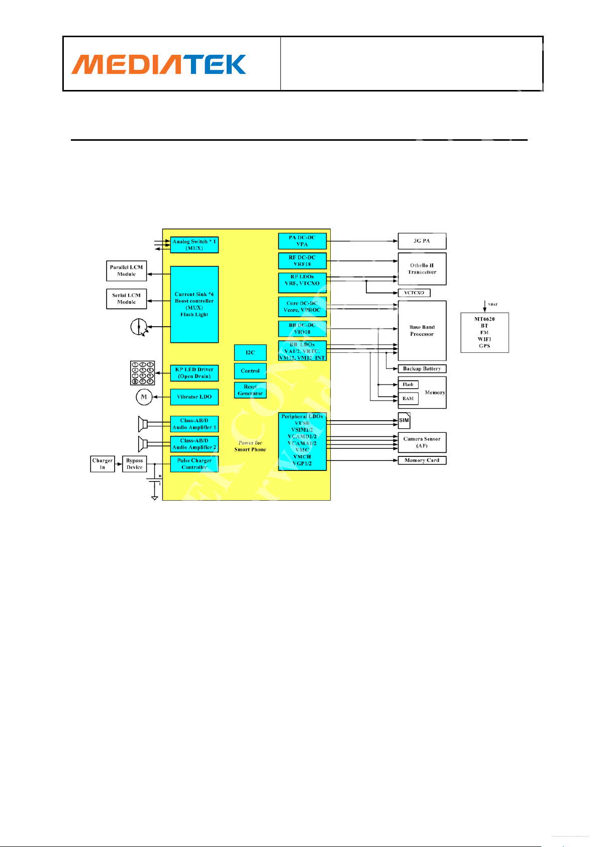
MT6329 is a fully integrated PMIC target for smart phone power provider. See Figure 2 the block
diagram for the whole picture of MT6329 PMIC.
Figure 2: MT6329 block diagram
3.2 PMIC Functional Blocks
MT6329 manages the power supply of the whole chip, such as the baseband, processor, memory,
SIM cards, camera, vibrator, etc. MT6329 includes the following analog functions for the use on smart
phone platforms.
LDO and BUCK: Provide regulated lower output voltage level from Li-Ion battery
Keypad/Flash LED driver (KPLED/FLASHLED) and current sink (ISINK) driver: Sink current for
keypad LED and LCM module
MEDIATEK CONFIDENTIAL
Controller: Generates power-on/off sequence, system reset and exceptional handling function
Charger controller: Controls/Protects battery charging procedure
Class-AB/D audio amplifier: Supports high-power/quality audio amplifier
Fuel gauge: Supports accurate battery capacity monitor
FOR zlixin@ waterworld.com.cn USE ONLY
This document contains information that is proprietary to MediaTek Inc.
Unauthorized reproduction or disclosure of this information in whole or in part is strictly prohibited.
MT6329
PMIC Datasheet
Confidential A
MediaTek Confidential
© 2011 - 2012 MediaTek Inc.
Page 26 of 97
UVLO
DDLO
VM12_1 / VM12_2
RESETB
PWRON
PWRKEY
VCORE
VPROC
VIO18
VIO28 / VM12_INT
VA1 / VA2
2ms
2ms
2ms
2ms
2ms
150ms
de-bounce
50ms
VRTC
PWRBB
VBAT
2ms
VMC / VMCH
2ms
VUSB / VTCXO
< 100ms
Free Datasheet http://www.datasheet4u.com/
More detailed descriptions of each sub-block are explained in the following sections.
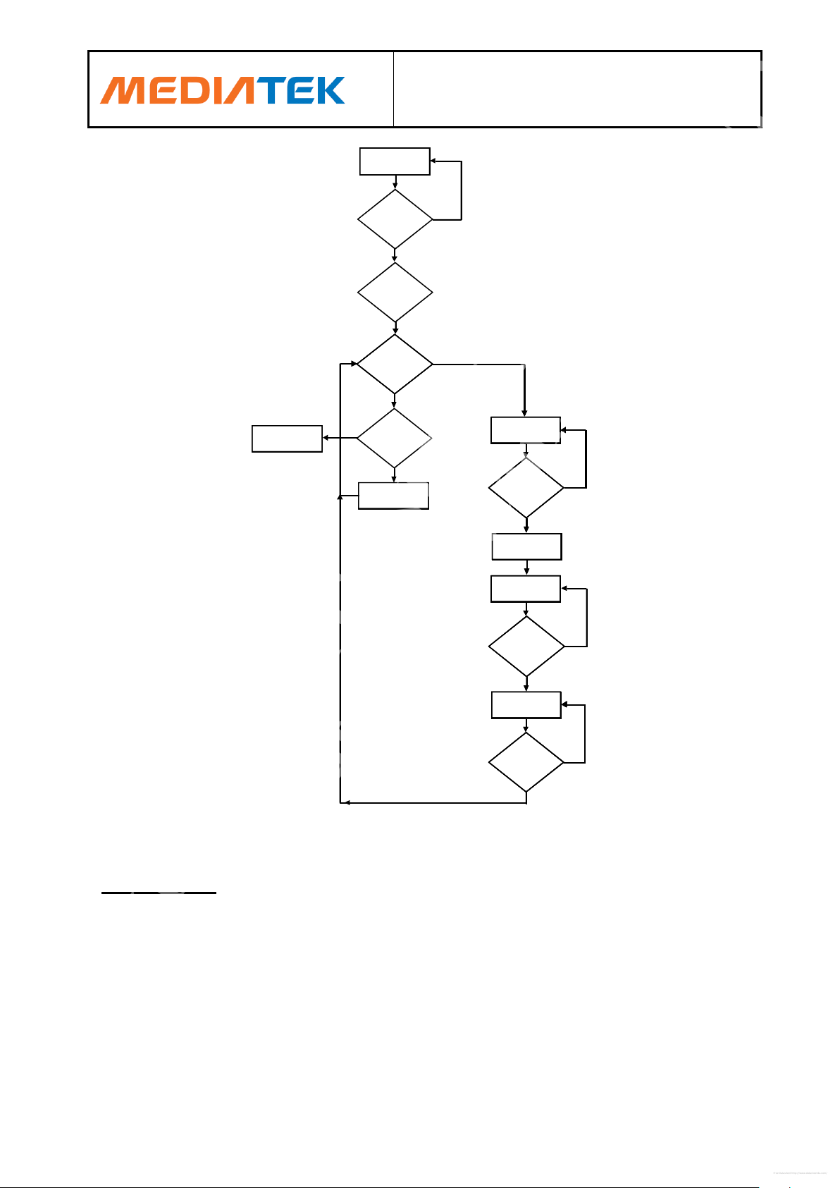
3.2.1 Power-On/Off Sequence
PMIC handles the powe-on and -off of the handset. If the battery voltage is neither in the UVLO state
(VBAT ≥ 3.4V) nor in the thermal condition, there are three methods to power on the handset system:
1) Pulling PWRKEY low (the user pushes PWRKEY), 2) Pulling PWRBB high (baseband BB_WakeUp)
and 3) Valid charger plug-in.
According to different battery voltage (VBAT) and phone state, control signals and regulators will have
different responses.
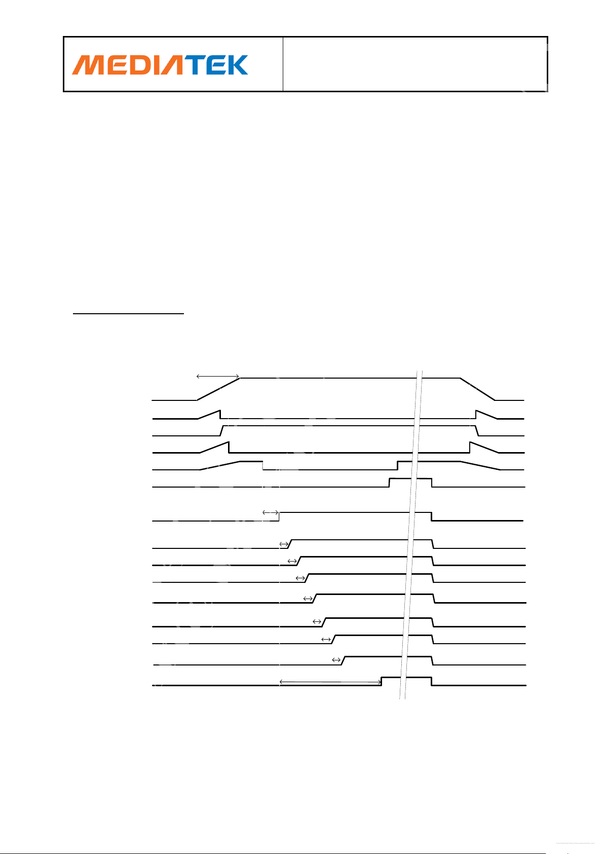
Power on/off sequence
The power-on/off sequence controlled by the “control” and “reset generator” is shown in the figure
below.
FOR zlixin@ waterworld.com.cn USE ONLY
MEDIATEK CONFIDENTIAL
Figure 3: Power-on/off control sequence by pressing PWRKEY
Unauthorized reproduction or disclosure of this information in whole or in part is strictly prohibited.
This document contains information that is proprietary to MediaTek Inc.

MT6329
PMIC Datasheet
Confidential A
MediaTek Confidential
© 2011 - 2012 MediaTek Inc.
Page 27 of 97
Free Datasheet http://www.datasheet4u.com/
Note that the figure above only shows one power-on/off. MT6329 handles the powe-on and -off of the
handset. The following three different ways methods switch on the handset (when VBAT ≥ 3.4V):
1. Pushing PWRKEY (pulling the PWRKEY pin to low level)
Pulling PWRKEY low is typical method to turn on the handset. The VCORE and VPROC buck
converters will be turned on first then VIO18 and VIO28 LDOs are turned on sequentially. The
supplies for the baseband are ready, and the system reset ends at the moment when all the
default-on regulators are fully turned on to ensure correct timing and function. After that, the
baseband sends the PWRBB signal back to PMIC for acknowledgement. To successfully power
on the handset, PWRKEY should be kept low until PMIC receives PWRBB from the baseband.
2. RTC module generates PWRBB to wake up the system
If the RTC module is scheduled to wake up the handset at some time, the PWRBB signal will be
directly sent to PMIC. In this case, PWRBB becomes high at specific moment and allows PMIC
power-on as the sequence described above. This is called the RTC alarm.
3. Valid charger plug-in (CHRIN voltage within valid range)
The charger plug-in will also turn on the handset if the charger is valid (no OVP takes place).
However, if the battery voltage is too low to power on the handset (UVLO state), the system will
not be turned on by any of the three methods. In this case, the charger will charge the battery first,
and the handset will be powered on automatically as long as the battery voltage is high enough.
Under-voltage lockout (UVLO)
The UVLO state in PMIC prevents start-up if the initial voltage of the main battery is below the 3.2V
threshold. It ensures that the handset is powered on with the battery in good condition. The UVLO
function is performed by a hysteretic comparator which ensures smooth power-on sequence. In
addition, when the battery voltage is getting lower, it will enter the UVLO stat,e and PMIC will be
turned off by itself, except for VRTC LDO, to prevent further discharging. Once PMIC enters the
UVLO state, it will draw low quiescent current. RTC LDO will still be working until DDLO disables it.
Deep discharge lockout (DDLO)
PMIC will enter the deep discharge lockout (DDLO) state when the battery voltage drops below 2.5V.
In this state, VRTC LDO will be shut down. Otherwise, it will draw very low quiescent current to
prevent further discharging or even damage to the cells.
Reset
PMIC contains a reset control circuit which takes effect at both power-up and power-down. The
RESETB pin is held low in the beginning of power-up and returns to high after the pre-determined
MEDIATEK CONFIDENTIAL
delay time. The delay time is controlled by a large counter, which uses the clock from the internal ringoscillator. At power-off, the RESETB pin will return to low immediately without any delay.
Over-temperature protection
FOR zlixin@ waterworld.com.cn USE ONLY
This document contains information that is proprietary to MediaTek Inc.
Unauthorized reproduction or disclosure of this information in whole or in part is strictly prohibited.
MT6329
PMIC Datasheet
Confidential A
MediaTek Confidential
© 2011 - 2012 MediaTek Inc.
Page 28 of 97
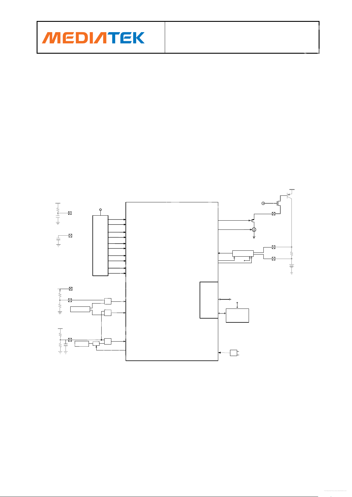
Rsense
VBAT
CHRIN
8V LDMOS
DRV
ISENSE
BATSNS
(VBAT)
gain
CCHRLDO_DET_CMP
VBGR
DXT790AP5
Charger Core
And
Digital Controller
CHRIN
3.3K
1u
1u
CHRLDO28
VREF
CHR_LDO_DET
CHR_LDO_DET
Interface
BC1.1
Controller
To BB
CSDAC_EN
CSDAC_DAT<7:0>
CS_DET
CS_EN
CS_VTH[3:0]
TREF
24k
RNTC
BATON
OTG_BVAILD_EN
CHRIN
VCDT UpTo 10.5V
330k
39k
VCDT
10uF
VBAT_DDLO_DET
VBAT_DDLO_VTH<1:0>
VBAT_UVLO_DET
VBAT_UVLO_VTH<1:0>
VBAT_CC_DET
VBAT_CC_VTH[1:0]
VBAT_CV_DET
VBAT_CV_VTH[1:0]
VBAT_OV_DET
VBAT_OV_VTH[1:0]
BATON_UNDET
OTG_BVALID_DET
VCDT_DET
VCDT_VTH[3:0]
NTR4503N
CHRLDO 2.8V
MUX
VTH CGRLDOGOOD
VBAT
Voltage
divider
VBAT
VCDT VREF GEN
OTG/BATON VREF GEN
COMP
COMP
COMP
Current
Sensing
EN vr
set
in1
in2
VREF
COMP
ON Chip
Off Chip
Charger block diagram
Free Datasheet http://www.datasheet4u.com/
If the die temperature of PMIC exceeds 150°C, PMIC will automatically disable all LDOs except for
VRTC. Once the over-temperature state is resolved, a new power-on sequence will be required to
enable the LDOs.
3.2.2 The Battery Charger (Charger Controller)
The charger controller senses the charger input voltage from either a standard AC-DC adaptor or an
USB charger. When the charger input voltage is within a pre-determined range, the charging process
will be activated. This detector resists higher input voltages than other parts of PMIC.
3.2.2.1 Block Descriptions
3.2.2.1.1 Charger Detection
Whenever an invalid charging source is detected (> 7.0V), the charger detector will stop the charging
process immediately to avoid burning out the chip or even the phone. Furthermore, if the charger-in
FOR zlixin@ waterworld.com.cn USE ONLY
MEDIATEK CONFIDENTIAL
This document contains information that is proprietary to MediaTek Inc.
Unauthorized reproduction or disclosure of this information in whole or in part is strictly prohibited.
Figure 4: PCHR block diagram

MT6329
PMIC Datasheet
Confidential A
MediaTek Confidential
© 2011 - 2012 MediaTek Inc.
Page 29 of 97
Free Datasheet http://www.datasheet4u.com/
level is not high enough (< 4.3V), the charger will also be disabled to avoid improper charging
behavior.
3.2.2.1.2 Charging Control
When the charger is active, the charger controller will manage the charging phase according to the
battery status. During the charging period, the battery voltage is constantly monitored. The battery
charger supports pre-charge mode (VBAT < 3.2V, PMIC power-off state), CC mode (constant current
mode or fast charging mode at the range of 3.2V < VBAT < 4.2V) and CV mode (constant voltage
mode) to optimize the charging procedure for Li-ion battery. See the figure below for the charging
states diagram.
FOR zlixin@ waterworld.com.cn USE ONLY
MEDIATEK CONFIDENTIAL
This document contains information that is proprietary to MediaTek Inc.
Unauthorized reproduction or disclosure of this information in whole or in part is strictly prohibited.
MT6329
PMIC Datasheet
Confidential A
MediaTek Confidential
© 2011 - 2012 MediaTek Inc.
Page 30 of 97
YES
CC Mode
VBAT > 4.1V
YES
NO
VBAT < 4.35V
Charger OFF
More than N times
FULL
YES
YES
NO
CHRIN > 4.3V
PreCC
YES
VBAT > 4.2V
YES
YES
CHRIN DET
VBAT > 3.3V
NON-CHARGING
Dead Battery
VBAT<2.2V
45 min timeout
NO
YES
VBAT < 3.3V
45 min timeout
NO
YES
CV Mode
CHRIN
Charger OFF
NO
NO
Free Datasheet http://www.datasheet4u.com/
Figure 5: Charging states diagram
Pre-charge mode
When the battery voltage is in the UVLO state, the charger will operate in the pre-charge mode. There
are two steps in this mode. While the battery voltage is deeply discharged below 2.2V, PRECC0
trickle charging current is applied to the battery.
MEDIATEK CONFIDENTIAL
The PRECC1 trickle charging current is about 56mA continuous current when VBAT is under 2.2V.
FOR zlixin@ waterworld.com.cn USE ONLY
This document contains information that is proprietary to MediaTek Inc.
Unauthorized reproduction or disclosure of this information in whole or in part is strictly prohibited.

MT6329
PMIC Datasheet
Confidential A
MediaTek Confidential
© 2011 - 2012 MediaTek Inc.
Page 31 of 97
Rsense
40mV
Rsense
V
I
SENSE
adapter ACPRECC2,
Rsense
14mV
Rsense
V
I
SENSE
HOSTUSB PRECC2,
Free Datasheet http://www.datasheet4u.com/
When the battery voltage exceeds 2.2V, i.e. the PRECC2 stage, the closed-loop pre-charge will be
enabled. The voltage drop across the external RSENSE is kept around 40mV (AC charger) or 14mV
(USB host). The closed-loop pre-charge current can be calculated:
Constant current mode
As the battery is charged up and over 3.3V, it can switch to the CC mode. (CHR_EN should be high)
In the CC mode, several charging currents can be set by programming registers or the external
RSENSE resistor. The charging current can be determined by CS_VTH/RSENSE, where CS_VTH is
programmed by registers. For example, if RSENSE is selected as 0.2ohm, the CC mode charging
current can be set from 70 to 800mA. It can accommodate the battery charger to various charger
inputs with different current capability.
Constant-voltage mode and over-voltage protection (OV)
While the battery voltage reaches about 4.2V, a constant current with much shorter period is used for
charging. It allows more often full battery detection in non-charging period. This is called the fullvoltage charging mode or constant-voltage charging mode in correspondence to a linear charger.
While the battery voltage actually reaches 4.2V, more than the pre-setting times within the limited
charging cycles, the end-of-charging process starts. It may prolong the charging and detecting period
for acquiring optimized full charging volume. The end of charging process is fully controlled by the
baseband and can be easily optimized for different battery packs. Once the battery voltage exceeds
4.35V, a hardware OV protection should be activated and turn off the charger immediately.
3.2.2.1.3 BC1.1 Dead-Battery Support of China Standard
MT6255 also support dead-battery condition from China standard (BC1.1). These specifications
protect dead-battery charging by timer and trickle current. Once the battery voltage is below 2.2V, a
period (TUNIT) of trickle current (IUNIT) will be applied to the battery.
If the battery voltage is still below 2.2V after applying the trickle current, the charger will be disabled.
On the other hand, once if the battery voltage rises up to above 2.2V, the charger will enter the
PRECC1 stage, and the charging current will be 70mA or 200mA depending on the type of the
charging port.
Under the condition of battery voltage from 2.2V to 3.3V, the charger will charge the battery with the
PRECC1 current.
A dedicated 5 mins. (T1) timer will be timed out and disable the charger if the battery voltage is always
below 2.7V under charging. Another 35 mins. (T2) timer will also be timed out and disable the charger
if the battery voltage is always kept between 2.7V and 3.3V under charging.
FOR zlixin@ waterworld.com.cn USE ONLY
MEDIATEK CONFIDENTIAL
This document contains information that is proprietary to MediaTek Inc.
Unauthorized reproduction or disclosure of this information in whole or in part is strictly prohibited.

MT6329
PMIC Datasheet
Confidential A
MediaTek Confidential
© 2011 - 2012 MediaTek Inc.
Page 32 of 97
BUCK name
Vout (Volt)
Imax (mA)
Application
VCORE
0.75 ~ 1.3 (25mV/step)
1,000
Digital CORE
VPROC/Vcore2
0.75 ~ 1.3 (25mV/step)
1,500
Processor
VIO18
1.8
1,000
IO
VRF_1V8
1.825
250
RF chip
V3GPA
0.9 ~ 3.4 (0.1V/step)
800
3G power amplifier
Free Datasheet http://www.datasheet4u.com/
The trickle current (IUNIT) and two dedicated timers protect the charging action if the battery is dead.
3.2.3 Buck Converter
There are 5 buck converters in MT6329 to efficiently generate regulated power for processor, digital
core, 3G power amplifier, memory IO and RF circuit. The block diagram is shown in Figure 10. The
buck converters operate with typically 2 MHz fixed frequency pulse width modulation (PWM) mode at
moderate to heavy load currents. At light load currents, the converter automatically enters pulse
frequency modulation (PFM) mode to save power and improve light load efficiency. It also has a forcePWM mode option to allow the converter to remain in the PWM mode regardless of the load current,
so that the noise spectrum of the converter can be minimized for certain highly-noise-sensitive
handset applications. The buck converters also have an internal over-current protection (OCP) circuit
to limit the maximum high-side power FET current in over-load conditions. It has an internal soft start
circuit to control the ramp-up rate of the output voltage during start-up.
Table 10: Buck converter brief specifications
1. Processor power, VPROC
VPROC is a high-current buck converter to provide a highly-efficient power supply for the handset
processor. Powering from a Li-ion battery, VPROC steps down the input voltage from 3.4 ~ 4.3V
to the typical output voltage of 1.2V with a maximum load current capability of 1.2A. The output
voltage can be adjusted between 0.7V and 1.3V. In order to optimize the overall system efficiency
for the processor, VPROC features a Dynamic Voltage Frequency Scaling (DVFS) function which
allows it to dynamically adjust its output voltage between 0.9V and 1.2V under different voltage
supply demands from the processor. For more details, refer to the “Dynamic Voltage Frequency
Scaling (DVFS)” section.
2. Digital CORE power, VCORE
VCORE is a high-current buck converter to provide a highly-efficient power supply for the handset
digital core. Powering from a Li-ion battery, VCORE steps down the input voltage from 3.4 ~ 4.3V
to the typical output voltage of 1.1V with a maximum load current capability of 1.0A. The output
voltage can be adjusted between 0.7V and 1.3V. In order to optimize the overall system efficiency
MEDIATEK CONFIDENTIAL
for digital core, VCORE features a Dynamic Voltage Frequency Scaling (DVFS) function which
allows it to dynamically adjust its output voltage between 0.9V and 1.1V under different voltage
supply demands from the digital core circuit. For more details, refer to the “Dynamic Voltage
Frequency Scaling (DVFS)” section.
FOR zlixin@ waterworld.com.cn USE ONLY
This document contains information that is proprietary to MediaTek Inc.
Unauthorized reproduction or disclosure of this information in whole or in part is strictly prohibited.

MT6329
PMIC Datasheet
Confidential A
MediaTek Confidential
© 2011 - 2012 MediaTek Inc.
Page 33 of 97
RG_VCORE_CTRL
Default:0
RG_VCORE_VOSEL
RG_VCORE_VOSEL_CON1
RG_VCORE_VOSEL
QI_VCORE_VOSEL[4:0]
0
1
0
1
SRCLKEN
0
1
RG_VCORE_VOSEL_SFCHG_EN
Default:0
SOFT_CHG
Free Datasheet http://www.datasheet4u.com/
3. IO & memory power, VIO18
VIO18 is a high-current buck converter to provide a highly-efficient power supply for the handset
I/O power. Powering from a Li-ion battery, VIO18 steps down the input voltage from 3.4 ~ 4.3V to
the typical output voltage of 1.8V with a maximum load current capability of 1.0A.
4. 3G PA power, VPA
VPA regulator is a DC-DC step-down converter which provides 0.9V to 3.4V programmable output
voltage (0.1V per step) and sources 800mA current at 3.4V and 150mA at 0.9V. In addition, its
output voltage can be configured at 1.35V by register settings. It provide 600mA current at 1.35V
and 1.5V output voltage to support DDRIII applications.
5. RF power, VRF18
VRF18 is a buck converter to provide a highly-efficient power supply for the handset RF power.
Powering from a Li-ion battery, VRF18 steps down the input voltage from 3.4 ~ 4.3V to the typical
output voltage of 1.825V with a maximum load current capability of 0.25A.
3.2.4 DVFS Control (Dynamic Voltage Frequency Scaling)
VCORE1, VPROC and VM12_INT have DVFS control respectively. There are two DVS modes: 1)
One-shot mode: If DVFS is issued, the voltage will directly jump to the target one. 2) Soft-change
mode: If DVFS is issued, the voltage will be switched step by step. See the figure below for the
VCORE DVFS voltage control logic:
There are two control modes:
1. Direct control by register (when @RG_VCORE_CTRL = 0)
2. Auto switch between normal operation mode and sleep mode voltage (when
@RG_VCORE_CTRL = 1)
See the figure below for the VPROC DVFS voltage control logic:
MEDIATEK CONFIDENTIAL
FOR zlixin@ waterworld.com.cn USE ONLY
This document contains information that is proprietary to MediaTek Inc.
Unauthorized reproduction or disclosure of this information in whole or in part is strictly prohibited.

MT6329
PMIC Datasheet
Confidential A
MediaTek Confidential
© 2011 - 2012 MediaTek Inc.
Page 34 of 97
RG_VPROC_CTRL[1:0]
Default:2`b00
RG_VPROC_VOSEL[4:0]
DVS1/0
00
01
1x
1
0
SRCLKEN
VPROC_VOSEL_SRCLKEN0[4:0]
VPROC_VOSEL_SRCLKEN1[4:0]
VPROC_VOSEL_DVS00[4:0]
VPROC_VOSEL_DVS01[4:0]
VPROC_VOSEL_DVS10[4:0]
VPROC_VOSEL_DVS11[4:0]
0
100
01
10
11
QI_VPROC_VOSEL[4:0]
0
1
RG_VPROC_VOSEL_SFCHG_EN
Default:0
SOFT_CHG
VPROC_VOSEL_PRE[4:0]
sfchg_out
RG_VM12_INT_CAL[4:0]
VM12_INT_LOW_BOUND[4:0]
VM12_INT_CTRL_SEL
Default :0
QI_VM12_INT_CAL[4:0]
0
1
0
1
SRCLKEN
VM12_INT_SLEEP[4:0]
<=
VPROC_VOSEL[4:0]
0
1
VPROC_VOSEL[4:0]
0
1
RG_VM12_INT_CAL_SFCHG_EN
Default:0
SOFT CHG
Free Datasheet http://www.datasheet4u.com/
There are three control modes:
1. Direct control by register (when @RG_VPROC_CTRL[1:0] = 00)
2. Auto switch between normal operation mode and sleep mode voltage (when
@RG_VPROC_CTRL[1:0] = 01)
3. Voltage control by dedicated pins DVS1 and DVS0. There are 4 dedicated registers for 4 DVS1,0
combinations. This mode enables fast voltage change to achieve better power and performance.
In addition, auto switch between normal operation and sleep mode voltage is still supported in the
mode. (when @RG_VPROC_CTRL[1:0] = 1x)
See the figure below for the VM12_INT DVFS voltage control logic:
There are two control modes:
1. Direct control by register (when @RG_VM12_INT_CTRL_SEL = 0)
2. Auto switch between normal operation mode and sleep mode voltage (when @
FOR zlixin@ waterworld.com.cn USE ONLY
RG_VM12_INT_CTRL_SEL = 1). Note that due to VM12_INT is for CPU internal SRAM power
which needs to track the VPROC voltage, the hardware auto tracking logic is implemented in this
mode. However, it has lower bound during operation to achieve normally access, there is
MEDIATEK CONFIDENTIAL
hardware auto low-voltage limit for this control logic.
This document contains information that is proprietary to MediaTek Inc.
Unauthorized reproduction or disclosure of this information in whole or in part is strictly prohibited.

MT6329
PMIC Datasheet
Confidential A
MediaTek Confidential
© 2011 - 2012 MediaTek Inc.
Page 35 of 97
VREF
VOUT
R1
R2
Current
Limit
Discharge
Control
AVDD43_VXX
VOUT
VOUT
GND
Type
LDO name
Vout (Volt)
Imax (mA)
Application
ALDO
VRF/VRF28
2.85
200
RF chip
ALDO
VTCXO
2.8
40
13/26 MHz reference clock
Free Datasheet http://www.datasheet4u.com/
3.2.5 Low Dropout Regulator (LDOs) and Reference
MT6329 integrates 21 LDOs optimized for their given functions by balancing quiescent current,
dropout voltage, line/load regulation, ripple rejection and output noise.
A low-dropout regulator (LDO) is capable of maintaining its specified output voltage over a wide range
of load current and input voltage, down to a very small difference between input and output voltages.
There are several features in the design of LDO, including discharge control, soft start and current
limit. Before LDO is enabled, the output pin of LDO should be discharged first to avoid voltage
accumulation on the capacitance. Soft-start limits inrush current and controls output-voltage rise time
during power-up. Current limit is the current protection to limit LDO’s output current and power
dissipation.
There are three types of LDOs in the MT6329 PMIC. The analog LDO is optimized for low-frequency
ripple rejection in order to reject the ripple coming from the burst of RF power amplifier. The digital IO
LDO is a linear regulator optimized for very low quiescent current. The single-step RTC LDO is a
linear regulator that can charge up a capacitor-type backup coin cell, which also supplies the RTC
module even at the absence of the main battery. The single-step LDO features the reverse current
protection and is optimized for ultra-low quiescent current while sustaining the RTC function as long
as possible.
MEDIATEK CONFIDENTIAL
FOR zlixin@ waterworld.com.cn USE ONLY
Figure 6: LDO block diagram
Table 11: LDO types and brief specifications
This document contains information that is proprietary to MediaTek Inc.
Unauthorized reproduction or disclosure of this information in whole or in part is strictly prohibited.

MT6329
PMIC Datasheet
Confidential A
MediaTek Confidential
© 2011 - 2012 MediaTek Inc.
Page 36 of 97
Type
LDO name
Vout (Volt)
Imax (mA)
Application
ALDO
VA1
1.8/2.0/2.1/2.5
100
Analog baseband
ALDO
VA2
2.5/2.8
100
Analog baseband
ALDO
VCAMA
1.5/1.8/2.5/2.8
200
Analog power for camera module
DLDO
VM12_1
1.2
300
DRAM
DLDO
VM12_2
1.2/1.1/1.0/0.9
300
DRAM or AST3001
DLDO
VM12_INT
1.2
360
SRAM
DLDO
VIO28
2.8
100
Digital IO
DLDO
VSIM1
1.8/3.0
100
1st SIM card
DLDO
VSIM2
1.3/1.5/1.8/2.5
2.8/3.0/3.3
100
2nd SIM card
DLDO
VUSB
3.3
100
USB
DLDO
VCAMD
1.3/1.5/1.8/2.5
2.8/3.0/3.3
300
Digital power for camera module
DLDO
VCAM_IO
1.3/1.5/1.8/2.5
2.8/3.0/3.3
100
IO power for camera module
DLDO
VCAM_AF
1.3/1.5/1.8/2.5
2.8/3.0/3.3
200
Auto-focus power for camera module
DLDO
VMC
1.3/1.5/1.8/2.5
2.8/3.0/3.3
200
Memory card
DLDO
VMCH
1.3/1.5/1.8/2.5
2.8/3.0/3.3
400
SD3.0 memory card
DLDO
VGP1
1.3/1.5/1.8/2.5
2.8/3.0/3.3
100
1st general-purpose LDO
DLDO
VGP2
1.3/1.5/1.8/2.5
2.8/3.0/3.3
100
2nd general-purpose LDO
DLDO
VIBR
1.3/1.5/1.8/2.5
2.8/3.0/3.3
200
Vibrator
RTCLDO
VRTC
1.8/2.0/2.1/2.8
2
Real-time clock
Free Datasheet http://www.datasheet4u.com/
1. Digital IO LDO (VIO28)
The digital IO LDO is a regulator that sources 100 mA (max.) with fixed 2.8V output voltage. The
LDO supplies the BB circuitry in the handset and is optimized for a very low quiescent current.
The VIO28 LDO is powered on as soon as the system enters the switched-on/stand-by mode.
Besides, the output voltage/current will fold-back as over-current/hard-short occurs.
2. Digital camera LDO (VCAMD)
The digital camera LDO is a regulator that sources 300 mA (max.) with programmable output
voltage. The LDO supplies the camera circuitry in the handset and is optimized for a lowquiescent current. VCAMD LDO can be enabled through the I2C interface. Besides, the foldedback OC protection is also available.
MEDIATEK CONFIDENTIAL
3. Digital camera auto focus LDO (VCAM_AF)
The digital camera auto focus LDO is a regulator that sources 200 mA (max.) with programmable
output voltage. The LDO supplies the camera auto focus circuitry in the handset and is optimized
FOR zlixin@ waterworld.com.cn USE ONLY
This document contains information that is proprietary to MediaTek Inc.
Unauthorized reproduction or disclosure of this information in whole or in part is strictly prohibited.

MT6329
PMIC Datasheet
Confidential A
MediaTek Confidential
© 2011 - 2012 MediaTek Inc.
Page 37 of 97
Free Datasheet http://www.datasheet4u.com/
for a low-quiescent current. VCAM_AF LDO can be enabled through the I2C interface. Besides,
the folded-back OC protection is also available.
4. Digital camera IO power LDO (VCAM_IO)
The digital camera IO power LDO is a regulator that sources 100 mA (max.) with programmable
output voltage. The LDO supplies the camera IO circuitry in the handset and is optimized for a
low-quiescent current. VCAM_IO LDO can be enabled through the I2C interface. Besides, the
folded-back OC protection is also available.
5. Vibrator power LDO (VIBR)
The vibrator power LDO is a regulator that sources 200 mA (max.) with programmable output
voltage. The LDO supplies the vibrator circuitry in the handset and is optimized for a lowquiescent current. VIBR LDO can be enabled through the I2C interface. Besides, the folded-back
OC protection is also available.
6. Memory card power LDO (VMC)
The memory card power LDO is a regulator that sources 200 mA (max.) with programmable
output voltage. The LDO supplies the memory card circuitry in the handset and is optimized for a
low-quiescent current. VMC LDO can be enabled through the I2C interface. Besides, the foldedback OC protection is also available.
7. SD3.0 memory card power LDO (VMCH)
The SD3.0 memory card power LDO is a regulator that sources 400 mA (max.) with
programmable output voltage. The LDO supplies the SD3.0 memory card circuitry in the handset
and is optimized for a low-quiescent current. VMCH LDO can be enabled through the I2C
interface. Besides, the folded-back OC protection is also available.
8. SIM LDO (VSIM1)
The SIM LDO is a regulator that sources 100 mA (max.) with 1.8 V or 3.0 V output voltages based
on the supply specs of subscriber identity module (SIM) card. The VSIM1 LDO supplies the SIMs
in the handset and is controlled independently of the other LDOs. Besides, the folded-back OC
protection is also available.
9. 2nd SIM LDO (VSIM2)
The SIM LDO is a regulator that sources 100 mA (max.) with programmable output voltages
based on the supply specs of subscriber identity module (SIM) card. The VSIM2 LDO supplies the
second SIM card in the handset and is controlled independently of the other LDOs. Besides, the
folded-back OC protection is also available.
10. Memory 1.2V LDO (VM12_1)
MEDIATEK CONFIDENTIAL
The memory 1.2V LDO is a regulator that sources 300 mA (max.) with fixed 1.2V output voltage.
The LDO supplies 1.2V to memory circuitry in the handset and is optimized for a low-quiescent
current. The VM12_1 LDO can be enabled through the I2C interface. Besides, the folded-back
OC protection is also available.
FOR zlixin@ waterworld.com.cn USE ONLY
This document contains information that is proprietary to MediaTek Inc.
Unauthorized reproduction or disclosure of this information in whole or in part is strictly prohibited.

MT6329
PMIC Datasheet
Confidential A
MediaTek Confidential
© 2011 - 2012 MediaTek Inc.
Page 38 of 97
Free Datasheet http://www.datasheet4u.com/
11. Reserve 1.2V power LDO (VM12_2)
The reserved 1.2V power LDO is a regulator that sources 300 mA (max.) with programmable
output voltage. The LDO supplies the reserved 1.2V power for AST3001 core circuitry in the
handset and is optimized for a low-quiescent current. VM12_2 LDO can be enabled through the
I2C interface. Besides, the folded-back OC protection is also available.
12. SRAM 1.2V power LDO (VM12_INT)
The SRAM 1.2V power LDO is a regulator that sources 360 mA (max.) with programmable output
voltage. The LDO supplies the SRAM circuitry in the handset and is optimized for a low-quiescent
current. VM12_INT LDO can be enabled through the I2C interface. Besides, the folded-back OC
protection is also available.
13. Analog camera LDO (VCAMA)
The analog camera LDO is a regulator that sources 200 mA (max.) with programmable
1.5/1.8/2.5/2.8V output voltage. The LDO supplies the camera circuitry in the handset and is
optimized for a very low frequency ripple rejection in order to reject the ripple coming from the
burst of RF power amplifier at 217 Hz. VCAMA LDO can be enabled through the I2C interface.
Besides, the folded-back OC protection is also available.
14. Analog LDO (VA1)
The analog LDO is a regulator that sources 200 mA (max.) with fixed 2.5V output voltage. The
LDO supplies the analog sections of the BB chipsets and is optimized for low-frequency ripple
rejection in order to reject the ripple coming from the burst of RF power amplifier at 217 Hz. VA
LDO is powered on as soon as the system enters the switched-on/stand-by mode. Besides, the
output voltage/current will fold-back as over-current/hard-short occurs.
15. Analog LDO (VA2)
The analog LDO2 is a regulator that sources 100 mA (max.) with fixed 2.5V output voltage. The
LDO supplies the analog sections of the BB chipsets and is optimized for low-frequency ripple
rejection in order to reject the ripple coming from the burst of RF power amplifier at 217 Hz. VA2
LDO is powered on as soon as the system enters the switched-on/stand-by mode. Besides, the
output voltage/current will fold-back as over-current/hard-short occurs.
16. TCXO LDO (VTCXO)
TCXO LDO is a regulator that sources 40 mA (max.) with a 2.8V output voltage. The LDO supplies the
temperature compensated crystal oscillator, which needs its own ultra-low noise supply and very good
ripple rejection ratio.
17. RF LDO (VRF)
MEDIATEK CONFIDENTIAL
The analog LDO is a regulator that sources 200 mA (max.) with fixed 2.85V output voltage. The
LDO supplies the RF circuitry in the handset and is optimized for low-frequency ripple rejection in
order to reject the ripple coming from the burst of RF power amplifier at 217 Hz.
FOR zlixin@ waterworld.com.cn USE ONLY
This document contains information that is proprietary to MediaTek Inc.
Unauthorized reproduction or disclosure of this information in whole or in part is strictly prohibited.

MT6329
PMIC Datasheet
Confidential A
MediaTek Confidential
© 2011 - 2012 MediaTek Inc.
Page 39 of 97
Free Datasheet http://www.datasheet4u.com/
18. General-purpose LDO (VGP1)
The general-purpose LDO is a regulator that sources 100 mA (max.) with programmable output
voltage. The LDO supplies the camera circuitry in the handset and is optimized for a very low
quiescent current. VGP LDO can be enabled through the I2C interface. Besides, the folded-back
OC protection is also available.
19. General-purpose LDO2 (VGP2)
The general-purpose LDO2 is a regulator that sources 100 mA (max.) with programmable output
voltage. The LDO supplies the camera circuitry in the handset and is optimized for a very low
quiescent current. VGP2 LDO can be enabled through the I2C interface. Besides, the folded-back
OC protection is also available.
20. USB LDO (VUSB)
The digital IO LDO is a regulator that sources 100 mA (max.) with fixed 3.3V output voltage. The
LDO supplies the BB circuitry in the handset and is optimized for a very low quiescent current.
VIO LDO is powered on as soon as the system enters the switched-on/stand-by mode. Besides,
the output voltage/current will fold-back as over-current/hard-short occurs.
21. RTC LDO (VRTC)
PMIC features a 2-step RTC that keeps RTC alive for a long time after the battery has been
removed. The first LDO charges a backup battery on the BAT_BACKUP pin to ~ 2.8V. In addition,
when the battery is removed, the first stage prevents the backup battery from leaking back to
VBAT. The second LDO regulates the 2.8V supply to a 1.5V/1.2V optional RTC voltage. The RTC
voltage can be set by the VCORE_SEL pin while BB is alive. The setting is retained while BB is
powered down. When the backup battery is fully charged, the high backup battery voltage, low
reverse current leakage and the low second LDO operating current sustain the RTC block for
even tens of hours with the absence of the main battery.
22. Reference voltage output (VREF)
The reference voltage output is a low-noise, high-PSRR and high-precision reference with a
guaranteed accuracy of 1.5% over temperature. The output is used as the system’s reference for
MT6329 internally. For accurate regulator and charger output voltage, DO NOT load the reference
voltage. Bypass it to GND with a minimum 100nF external capacitor.
3.2.6 Drivers
MT6329 supports backlight LED drivers both in parallel and in series configurations by pin sharing
ISINK and boost controller circuits. Besides, it provides the drivers for keypad LED and Flash light
LED. The following two figures depict two major applications for backlight LEDs and other drivers.
FOR zlixin@ waterworld.com.cn USE ONLY
MEDIATEK CONFIDENTIAL
This document contains information that is proprietary to MediaTek Inc.
Unauthorized reproduction or disclosure of this information in whole or in part is strictly prohibited.

MT6329
PMIC Datasheet
Confidential A
MediaTek Confidential
© 2011 - 2012 MediaTek Inc.
Page 40 of 97
VBAT
ISINK0
ISINK1
ISINK2
ISINK3
ISINK4
ISINK5
Dimming Controlled
By PWM1,2 or 3
Free Datasheet http://www.datasheet4u.com/
Figure 7: Configuration for parallel BL LED drivers
3.2.6.1 Backlight (B.L.) LED Driver
For parallel configuration, MT6329 supports up to 6 LEDs in parallel with 6-step programmable
current in each channel. The B.L. LEDs are supplied by the battery voltage. The LED current are
FOR zlixin@ waterworld.com.cn USE ONLY
Figure 8: Configuration for serial BL LED drivers
MEDIATEK CONFIDENTIAL
This document contains information that is proprietary to MediaTek Inc.
Unauthorized reproduction or disclosure of this information in whole or in part is strictly prohibited.

MT6329
PMIC Datasheet
Confidential A
MediaTek Confidential
© 2011 - 2012 MediaTek Inc.
Page 41 of 97
FLASH DRIVER
PAD_FLASH
RG_FLASH_EN
RG_FLASH_STEP[2:0]
Free Datasheet http://www.datasheet4u.com/
controlled by the current sinks in MT6329. The brightness of the B.L. LEDs can be controlled by
tuning the current for current sinks or switching on/off the current sinks through dimming control. The
dimming frequency and duty can be programmed by registers through the I2C interface. For more
details, refer to the “Dimming Control” section.
For series configuration, MT6329 internal boost controller supports 20mA for up to 10 LEDs in series.
External ballast resistor is necessary and serially connected between the LED string and ground. The
voltage across the external ballast resistor is used to feedback the BL LED current information to the
boost controller of MT6329. The BL LED current is regulated by the negative feedback loop formed in
the boost controller. In addition, the brightness of the B.L. LEDs can be controlled by changing the
external ballast resistors, tuning the feedback voltage (analog dimming) or switching on/off the boost
controller through dimming control (digital dimming). The analog/digital dimming selection, dimming
frequency and duty can be programmed by registers through the I2C interface. For more details on
digital dimming, refer to the “Dimming Control” section.
3.2.6.2 Flash Light LED Driver
The flash light LED driver is a low Ron switch which allows up to 500mA current. The brightness of the
flash light LED can be controlled by changing the external series ballast resistor.
3.2.6.3 Keypad LED Driver
The keypad LED driver is a low Ron switch which allows up to 150mA current. The brightness of the
keypad LED can be controlled by changing the external series ballast resistor.
FOR zlixin@ waterworld.com.cn USE ONLY
Figure 9: Configuration for flash light LED driver
MEDIATEK CONFIDENTIAL
This document contains information that is proprietary to MediaTek Inc.
Unauthorized reproduction or disclosure of this information in whole or in part is strictly prohibited.

MT6329
PMIC Datasheet
Confidential A
MediaTek Confidential
© 2011 - 2012 MediaTek Inc.
Page 42 of 97
KPLED DRIVER
PAD_KPLED
RG_KPLED_EN
RG_KPLED_STEP[2:0]
Free Datasheet http://www.datasheet4u.com/
Figure 10: Configuration for KP LED driver
3.2.6.4 Dimming Control
The intensity of the backlight WLED, flash light LED, keypad LED and vibrator can be adjusted by
dimming control. Although they can be controlled separately, the concepts are the same. It can be
controlled by programming some internal registers to change the on/offF pulse duty cycle and
frequency.
3.2.6.4.1 Pulse Duty Cycle
For all drivers, the output duty cycle is adjusted by selecting the corresponding driver’s PWM_DUTY
value according to the following relationship:
(VIBR/KP/FLASH/BL) PWM duty cycle = (PWM_DUTY + 1) high’s , and 32 - (PWM_DUTY +1) low’s
, where PWM_DUTY ranges from 0 to 31.
3.2.6.4.2 Frequency
For all drivers, the output frequency is changed by adjusting the corresponding driver’s PWM_DIV
value according to the following relationship:
(VIBR/KP/FLASH/BL) PWM frequency = 1.4M/25/(PWM_DIV + 1)/32
, where PWM_DIV ranges from 0 to15.
For FLASH/BL, the output frequency is changed by adjusting PWM_DIV and BYPASS. The output
MEDIATEK CONFIDENTIAL
frequency is governed by:
When bypass = 0,
(FLASH/BL) PWM frequency = 1.4M/25/(PWM_DIV + 1)/32
FOR zlixin@ waterworld.com.cn USE ONLY
This document contains information that is proprietary to MediaTek Inc.
Unauthorized reproduction or disclosure of this information in whole or in part is strictly prohibited.

MT6329
PMIC Datasheet
Confidential A
MediaTek Confidential
© 2011 - 2012 MediaTek Inc.
Page 43 of 97
Driver Enable Duty Div Bypass
VIBR
○ ○ ○
KP
○ ○ ○
FLASH
○ ○ ○ ○
BL
○ ○ ○ ○
Free Datasheet http://www.datasheet4u.com/
When bypass = 1,
(FLASH/BL) PWM frequency = 1.4M/(PWM_DIV + 1)/32
, where PWM_DIV ranges from 0 to 15.
3.2.6.4.3 Summary
The features of each driver are listed in the table below. All drivers can be enabled, and their duty and
frequency can be adjusted. For FLASH and BL, the fixed divisor, 25, can be bypassed.
3.2.7 Analog Switch
MT6239 has a built-in 2-to-1 analog switch with less than 3 ohm turn-on resistance supporting both
microphone input and video line-out operation. THD is up to 70dB for microphone and good PSRR
which is around 75dB across the voice band. The low turn-on resistance ensures linearity of the video
playback.
3.2.8 Class-AB/D Audio Amplifier
MT6329 has built-in dual channel high efficiency class AB/D audio power amplifier capable of
delivering 1 watt of power to an 8 ohm (each channel, stereo) BTL load and up to 2 watts onto parallel
equivalent 4-ohm load (mono in two channels) from a 4.2V battery supply. The THD performance is
74/76dB for class-D/AB mode respectively. The input must be AC-coupled. Over-current protection is
integrated. MT6329 also has built-in receiver bypass function for 2-in-1 loudspeaker. This built–in
receiver bypass supports multi-purpose loudspeaker without any extra BOM cost. The output power
can reach 97mW onto 8 ohm speaker load. The block diagram is shown in Error! Reference source
not found..
MEDIATEK CONFIDENTIAL
FOR zlixin@ waterworld.com.cn USE ONLY
This document contains information that is proprietary to MediaTek Inc.
Unauthorized reproduction or disclosure of this information in whole or in part is strictly prohibited.

MT6329
PMIC Datasheet
Confidential A
MediaTek Confidential
© 2011 - 2012 MediaTek Inc.
Page 44 of 97
Speaker Amplifier
SPKR_P
Audio_R input
+
-
Class ABD
SPKR_N
Audio_L input
+
-
Class ABD
SPKL_P
SPKL_N
Voice input
Input MUX
Free Datasheet http://www.datasheet4u.com/
Figure 11: Block diagram of class-AB/D
3.2.9 Fuel Gauge
The fuel gauging system includes a dedicated ADC for Li-Ion battery current measurement and
utilizes the measurement ADC (AUXADC) for battery voltage and temperature measurement. The
battery state-of-charge (SOC) estimation is performed by the software using the three measuring
methods and the accumulated current measurement. The application diagram of the fuel gauging
system is shown in the figure below, where an external resistor is used to converter the current drawn
from the battery into a voltage which is then measured by FG ADC. The value of the external resistor
must be chosen so that the maximum current during charging or discharging will not cause ADC to
exceed its input voltage range.
The principle of operation of the fuel gauge relies on a combination of Coulomb counting and light
load battery voltage measurement. Coulomb counting provides an estimate of the charge that has
been withdrawn or delivered to the battery, while battery voltage measurement proves a good
estimate of the battery SOC under low-load conditions. The battery voltage measurement
compensates for error accumulation during the current integration inherent in Coulomb counting. The
hardware also includes necessary modes to allow for simultaneous current and voltage measurement
which can be utilized to estimate the battery impedance.
FOR zlixin@ waterworld.com.cn USE ONLY
MEDIATEK CONFIDENTIAL
This document contains information that is proprietary to MediaTek Inc.
Unauthorized reproduction or disclosure of this information in whole or in part is strictly prohibited.

MT6329
PMIC Datasheet
Confidential A
MediaTek Confidential
© 2011 - 2012 MediaTek Inc.
Page 45 of 97
Free Datasheet http://www.datasheet4u.com/
Figure 12: Fuel gauge block diagram and external connection
3.2.9.1 Over-Current and Interrupt
There are 7 groups of interrupts for MT6329 to inform BB IC:
1. Key pressed and released interrupt
PWRKEY: Interrupt is issued when PWRKEY is pressed (and released, set by the register).
After receiving the interrupt, the software will read the PWRKEY_DEB status to see if it is
pressed or released.
HOMEKEY: Interrupt is issued when HOMEKEY is pressed (and released, set by the register).
After receiving the interrupt, the software will read the HOMEKEY_DEB status to see if it is
pressed or released.
2. Thermal interrupt
MT6329 issues THR_H interrupt for the software high power latch if PMIC die temperature is over
125c and issues THR_L for software latch release if PMIC die temperature goes from 125c back
to under 110c.
FOR zlixin@ waterworld.com.cn USE ONLY
MEDIATEK CONFIDENTIAL
This document contains information that is proprietary to MediaTek Inc.
Unauthorized reproduction or disclosure of this information in whole or in part is strictly prohibited.

MT6329
PMIC Datasheet
Confidential A
MediaTek Confidential
© 2011 - 2012 MediaTek Inc.
Page 46 of 97
Free Datasheet http://www.datasheet4u.com/
3. Charger related interrupt
There are several interrupts supported for charger control:
CHRDET
OV
WATCHDOG
OTG_BVALID
VBATON_UNDET
4. Battery voltage/current H/L interrupt
There are two groups of VBAT detection interrupt.
1) VBAT detected by AUXADC
If VBAT is higher than the threshold specified by an register setting, the HIGHBATTERY
interrupt will be issued. If VBAT is lower than the threshold specified by another register
setting, the LOWBATTERY interrupt will be issued.
2) VBAT detected by fuel gauge
If VBAT is higher than the threshold specified by an register setting, the VBAT_H interrupt will
be issued. If VBAT is lower than the threshold specified by another register setting, the
VBAT_L interrupt will be issued.
5. Speaker OC interrupt
MT6329 supports speaker OC interrupt generation which uses PWM detection method.
6. BUCK OC interrupt
MT6329 supports VPA and VRF18 OC interrupt generation which uses PWM detection method.
MEDIATEK CONFIDENTIAL
7. LDO OC interrupt
MT6329 supports LDO OC interrupt generation. It will be issued if any one of the LDOs has OC
condition.
FOR zlixin@ waterworld.com.cn USE ONLY
This document contains information that is proprietary to MediaTek Inc.
Unauthorized reproduction or disclosure of this information in whole or in part is strictly prohibited.

MT6329
PMIC Datasheet
Confidential A
MediaTek Confidential
© 2011 - 2012 MediaTek Inc.
Page 47 of 97
Module name Interrupt Signal Name Level/Edge
STRUP PWRKEY_DEB_INT_FLAG RG_PWRKEY_INT_EN bank0, 0x16, bit 1
RG_PWRKEY_INT_STATUS bank0, 0x19, bit1 edge(rising & falling)
STRUP HOMEKEY_DEB_INT_FLAG RG_HOMEKEY_INT_EN bank0, 0x18, bit 5
RG_HOMEKEY_INT_STATUS bank0, 0x1B, bit5 edge(rising & falling)
STRUP THR_H_INT_FLAG RG_THR_H_INT_EN bank0, 0x16, bit 3
RG_THR_H_INT_STATUS bank0, 0x19, bit3 edge(rising)
STRUP THR_L_INT_FLAG RG_THR_L_INT_EN bank0, 0x16, bit 2
RG_THR_L_INT_STATUS bank0, 0x19, bit2 edge(falling)
Charger CHRDET_INT_FLAG RG_CHRDET_INT_EN bank0, 0x16, bit 6
RG_CHRDET_INT_STATUS bank0, 0x19, bit6 edge(rising & falling)
Charger OV_INT_FLAG RG_OV_INT_EN bank0, 0x16, bit 7
RG_OV_INT_STATUS bank0, 0x19, bit7 edge(rising)
Charger WATCHDOG_INT_FLAG RG_WATCHDOG_INT_EN bank0, 0x16, bit 0
RG_WATCHDOG_INT_STATUS bank0, 0x19, bit0 level
Charger OTG_BVALID RG_BVALID_DET_INT_EN bank0, 0x16, bit 5
RG_BVALID_DET_INT_STATUS bank0, 0x19, bit5 level
Charger VBATON_UNDET RG_VBATON_UNDET_INT_EN bank0, 0x16, bit 4
RG_VBATON_UNDET_INT_STATUS bank0, 0x19, bit4 level
Auxadc HIGHBATTERY_INT_FLAG RG_HIGH_BAT_INT_EN bank0, 0x17, bit 5
RG_HIGH_BAT_INT_STATUS bank0, 0x1A, bit5 level
Auxadc LOWBATTERY_INT_FLAG RG_LOW_BAT_INT_EN bank0, 0x17, bit 4
RG_LOW_BAT_INT_STATUS bank0, 0x1A, bit4 level
FGADC VBAT_H_INT_FLAG RG_FG_BAT_H_INT_EN bank0, 0x17, bit 7
RG_FG_BAT_H_INT_STATUS bank0, 0x1A, bit7 level
FGADC VBAT_L_INT_FLAG RG_FG_BAT_L_INT_EN bank0, 0x17, bit 6
RG_FG_BAT_L_INT_STATUS bank0, 0x1A, bit6 level
Speaker SPKR_D_OC_FLAG RG_SPKR_D_OC_INT_EN bank0, 0x17, bit 3
RG_SPKR_D_OC_INT_STATUS bank0, 0x1A, bit3 level
Speaker SPKL_D_OC_FLAG RG_SPKL_D_OC_INT_EN bank0, 0x17, bit 2
RG_SPKL_D_OC_INT_STATUS bank0, 0x1A, bit2 level
Speaker SPKR_AB_OC_FLAG RG_SPKR_AB_OC_INT_EN bank0, 0x17, bit 1
RG_SPKR_AB_OC_INT_STATUS bank0, 0x1A, bit1 level
Speaker SPKL_AB_OC_FLAG RG_SPKL_AB_OC_INT_EN bank0, 0x17, bit 0
RG_SPKL_AB_OC_INT_STATUS bank0, 0x1A, bit0 level
Regulator VRF18_OC_FLAG RG_VRF18_OC_INT_EN bank0, 0x18, bit 4
RG_VRF18_OC_INT_STATUS bank0, 0x1B, bit4 level
Regulator VPA_OC_FLAG RG_VPA_OC_INT_EN bank0, 0x18, bit 3
RG_VPA_OC_INT_STATUS bank0, 0x1B, bit3 level
Regulator LDO_OC_FLAG RG_LDO_OC_INT_EN bank0, 0x18, bit 2
RG_LDO_OC_INT_STATUS bank0, 0x1B, bit2 level
enable
status
Interrupt Signal Name default en? de-bounce time
Status Clear
Condition
PWRKEY_DEB_INT_FLAG 1 50ms (in STRUP) Write 1 Clear
HOMEKEY_DEB_INT_FLAG 0 50ms (in STRUP) Write 1 Clear
THR_H_INT_FLAG 0 40ms (in STRUP) Write 1 Clear
THR_L_INT_FLAG 0 40ms (in STRUP) Write 1 Clear
CHRDET_INT_FLAG 1 50ms (in STRUP) Read Clear
OV_INT_FLAG 1 4us (in PCHR_DIG) Read Clear
WATCHDOG_INT_FLAG 1 No Write 1 Clear
OTG_BVALID 1 0/100/200/400us (in INT_CTRL) Write 1 Clear
VBATON_UNDET 1 4us (in PCHR_DIG) Write 1 Clear
HIGHBATTERY_INT_FLAG 0 V (in AUXADC) Write 1 Clear
LOWBATTERY_INT_FLAG 0 V (in AUXADC) Write 1 Clear
VBAT_H_INT_FLAG 0 V (in FGADC) Write 1 Clear
VBAT_L_INT_FLAG 0 V (in FGADC) Write 1 Clear
SPKR_D_OC_FLAG 0 V (in SPK) Write 1 Clear
SPKL_D_OC_FLAG 0 V (in SPK) Write 1 Clear
SPKR_AB_OC_FLAG 0 V (in SPK) Write 1 Clear
SPKL_AB_OC_FLAG 0 V (in SPK) Write 1 Clear
VRF18_OC_FLAG 0 PMW deb (in INT_CTRL) Write 1 Clear
VPA_OC_FLAG 0 PMW deb (in INT_CTRL) Write 1 Clear
LDO_OC_FLAG 1
100/200/400/800us
(in INT_CTRL)
Write 1 Clear
Free Datasheet http://www.datasheet4u.com/
MT6329 interrupt tables:
3.2.9.2 Watchdog
Watchdog is used to monitor whether the baseband is still awake while charging. The user can set up
the time-out threshold by TIMEOUT_GEAR. They are 4s, 8s, 16s, and 32s respectively. The figure
below is the state diagram of watchdog. Watchdog timer starts to count when the charger enabling
register is set. If the software does not write the specific register within designated time, the watchdog
will time out and issue interrupts. It means that the watchdog is also one type of interrupt source in
addition to those described in 4.3.10.1. The software can select a proper time-out value by setting up
the time-out gear register. Like most of the interrupt mechanism mentioned above, the watchdog
interrupt is write-clear.
PMIC can start to charge only when the charger is detected, charger enabling register is set, and
watchdog is not timed-out. If one of the three conditions is false, the charging will be prohibited.
FOR zlixin@ waterworld.com.cn USE ONLY
MEDIATEK CONFIDENTIAL
This document contains information that is proprietary to MediaTek Inc.
Unauthorized reproduction or disclosure of this information in whole or in part is strictly prohibited.

MT6329
PMIC Datasheet
Confidential A
MediaTek Confidential
© 2011 - 2012 MediaTek Inc.
Page 48 of 97
IDLE
Never write RG_WATCHDOG_INT_FLAG_STATUS within 4/8/16/32 sec
&& RG_CHR_EN =1
TIMEOUT
CHARGER related
Watchdog:
Chr_en:
INT
RG
_
WATCHDOG
_
INT
_
FLAG
_
STATUS
=
1
Write RG
_
WATCHDOG
_
INT
_
FLAG
_
STATUS
IDLE CHARGING
CHR_EN=1 && CHRDET=1 && no TIMEOUT
CHR_EN=0 || CHRDET=0 || TIMEOUT
S Device AddressR/W Data
7 7 71 0 0 0
Write Sequence
P
Bit
… … …
AA AS Device AddressR/W Data
7 7 71 0 0 0
Write Sequence
P
Bit
… … …
AA A
Free Datasheet http://www.datasheet4u.com/
Figure 13: Watchdog
3.2.10 I2C Interface
PMIC uses a 2-wire interface consisting of a clock and data signals (SCL and SDA) to connect to BB.
This bi-directional serial bus interface allows BB to write commands to and read status from PMIC.
The SCL signal is driven by the master, whereas the SDA signal is bidirectional and can be driven by
either the master or slave.
3.2.10.1 Write Sequence
I2C write cycle:
“S” is the start bit as defined in I2C spec. “Device” is the device ID, and our device ID is “1100000”.
R/W is read/write flag of the following byte. 1 means read, and 0 means write. “A” is the
acknowledgement bit. “P” is the stop bit. The number below the blue bar is the bit order. The device
has 7 bits from 7 to 1, and bit 0 is R/W. The “Address” and “Data” both have 8 bits. After the write
sequence, the data in “Data” will be written to address “Address”.
MEDIATEK CONFIDENTIAL
3.2.10.2 Read Sequence
I2C read cycle:
FOR zlixin@ waterworld.com.cn USE ONLY
This document contains information that is proprietary to MediaTek Inc.
Unauthorized reproduction or disclosure of this information in whole or in part is strictly prohibited.

MT6329
PMIC Datasheet
Confidential A
MediaTek Confidential
© 2011 - 2012 MediaTek Inc.
Page 49 of 97
Constraint
Min.
Max.
Description
tF
25ns
100ns
Fall time
tR
25ns
100ns
Rise time
tHD
100ns
-
Hold time of SDA to SCL
S Device AddressR/W
7 71 0 0
Read Sequence
DataS Device R/W
7 71 0 0
P
Bit
… …
… …
A A
A A
S Device AddressR/W
7 71 0 0
Read Sequence
DataS Device R/W
7 71 0 0
P
Bit
… …
… …
A A
A A
t
F
t
R
tHDt
SU
t
HIGH
t
LOW
SCL
SDA
All signal
Free Datasheet http://www.datasheet4u.com/
The write sequence has 3 byte of data, but the read sequence has 4 bytes. In the read sequence, the
device and R/W are sent twice, and R/W is 0 (write) at the first time and 1 (read) at the second time.
There are also two start bits. The second start bit means the device will be sent again, and the
read/write mode can be switched. The address is sent from the host, and the data will be given from
the device.
3.2.10.1 Bank Address
There are two register banks: bank 0 and bank 1
Bank 0
Device address[7:1] = 0110000
Includes top, startup, interrupt, pulse charger, Buck, analog LDO, digital LDO and AUXADC related
control settings.
Bank 1
Device address[7:1] = 0110001
Includes test, driver, boost, speaker, analog switch, fuel gauge, OTP and I2C related control settings.
3.2.10.2 Timing Constraint
MEDIATEK CONFIDENTIAL
FOR zlixin@ waterworld.com.cn USE ONLY
This document contains information that is proprietary to MediaTek Inc.
Unauthorized reproduction or disclosure of this information in whole or in part is strictly prohibited.

MT6329
PMIC Datasheet
Confidential A
MediaTek Confidential
© 2011 - 2012 MediaTek Inc.
Page 50 of 97
Constraint
Min.
Max.
Description
tSU
100ns
-
Setup time of SDA to SCL
t
HIGH
100ns
-
Period when SCL is high
t
LOW
100ns
-
Period when SCL is low
SCL …… ……
SDA …… ……
START
W
Slave
ack
Slave
ack
Slave
ack
STOP
DEV[7:1]
ADDR[7:0]
DATA[7:0]
Address
Name
Widt
h
Register Function
21
CHR_CON0
8
Charger Control Register 0
Set this register for PMIC Charger circuit configuration controls.
22
CHR_CON1
8
Charger Control Register 1
23
CHR_CON2
8
Charger Control Register 2
Set this register for PMIC Charger circuit configuration controls.
24
CHR_CON3
8
Charger Control Register 3
25
CHR_CON4
8
Charger Control Register 4
Free Datasheet http://www.datasheet4u.com/
3.2.10.3 Example
(1) MTK’s register write protocol
(2) MTK’s register read protocol
3.2.10.4 Related Registers
SCL and SDA can be pulled high optionally by I2C_PULL_HIGH_B. If the master in baseband forces
to send 1 through SCL and SDA to slave, the slave can set I2C_PULL_HIGH_B to 1 (not pull high
internally) to save power. If the master only pulls SCL and SDA high internally, I2C_PULL_HIGH_B
must be set to 0 to meet the I2C protocol.
3.3 Register Table and Descriptions
3.3.1 Bank 0
MEDIATEK CONFIDENTIAL
This document contains information that is proprietary to MediaTek Inc.
FOR zlixin@ waterworld.com.cn USE ONLY
Unauthorized reproduction or disclosure of this information in whole or in part is strictly prohibited.

MT6329
PMIC Datasheet
Confidential A
MediaTek Confidential
© 2011 - 2012 MediaTek Inc.
Page 51 of 97
Set this register for PMIC Charger circuit configuration controls.
27
CHR_CON6
8
Charger Control Register 6
Set this register for PMIC Charger circuit configuration controls.
28
CHR_CON7
8
Charger Control Register 7
2B
CHR_CONA
8
Charger Control Register 10
Set this register for PMIC Charger circuit configuration controls.
2E
CHR_COND
8
Charger Control Register 13
30
CHR_CONF
8
Charger Control Register 15
44
VPROC_CON5
8
VPROC Control Register 5
45
VPROC_CON6
8
VPROC Control Register 6
47
VPROC_CON8
8
VPROC Control Register 8
48
VPROC_CON9
8
VPROC Control Register 9
49
VPROC_CONA
8
VPROC Control Register A
4A
VPROC_CONB
8
VPROC Control Register B
4B
VPROC_CONC
8
VPROC Control Register C
57
VCORE_CON5
8
VCORE Control Register 5
59
VCORE_CON7
8
VCORE Control Register 7
60
VRF18_CON3
8
VRF18 Control Register 3
73
VPA_CON3
8
VPA Control Register 3
75
VPA_CON5
8
VPA Control Register 5
76
VPA_CON6
8
VPA Control Register 6
77
VPA_CON7
8
VPA Control Register 7
78
VPA_CON8
8
VPA Control Register 8
79
VPA_CON9
8
VPA Control Register 9
7A
VPA_CONA
8
VPA Control Register A
7B
VPA_CONB
8
VPA Control Register B
7C
VPA_CONC
8
VPA Control Register C
7D
VPA_COND
8
VPA Control Register D
7E
VPA_CONE
8
VPA Control Register E
7F
VPA_CONF
8
VPA Control Register F
83
DIGLDO_CON1
8
Digital LDO Control Register 1
87
DIGLDO_CON5
8
Digital LDO Control Register 5
95
DIGLDO_CON13
8
Digital LDO Control Register 13
98
DIGLDO_CON16
8
Digital LDO Control Register 16
9E
DIGLDO_CON1C
8
Digital LDO Control Register 1C
A1
DIGLDO_CON1F
8
Digital LDO Control Register 1F
A4
DIGLDO_CON22
8
Digital LDO Control Register 22
A7
DIGLDO_CON25
8
Digital LDO Control Register 25
AB
DIGLDO_CON29
8
Digital LDO Control Register 29
AF
DIGLDO_CON2D
8
Digital LDO Control Register 2D
B2
DIGLDO_CON30
8
Digital LDO Control Register 30
B5
DIGLDO_CON33
8
Digital LDO Control Register 33
B7
DIGLDO_CON35
8
Digital LDO Control Register 35
B8
DIGLDO_CON36
8
Digital LDO Control Register 36
BA
DIGLDO_RSV
8
Reserved register
Free Datasheet http://www.datasheet4u.com/
MEDIATEK CONFIDENTIAL
This document contains information that is proprietary to MediaTek Inc.
Unauthorized reproduction or disclosure of this information in whole or in part is strictly prohibited.
FOR zlixin@ waterworld.com.cn USE ONLY

MT6329
PMIC Datasheet
Confidential A
MediaTek Confidential
© 2011 - 2012 MediaTek Inc.
Page 52 of 97
BE
ANALDO_CON1
8
Analog LDO Control Register 1
C1
ANALDO_CON4
8
Analog LDO Control Register 4
C8
ANALDO_CONB
8
Analog LDO Control Register B
CB
ANALDO_CONE
8
Analog LDO Control Register E
D0
ANALDO_CON13
8
Analog LDO Control Register 13
DA
AUXADC_CON0
8
AUXADC Control Register 0
DB
AUXADC_CON1
8
AUXADC Control Register 1
DC
AUXADC_CON2
8
AUXADC Control Register 2
DD
AUXADC_CON3
8
AUXADC Control Register 3
DE
AUXADC_CON4
8
AUXADC Control Register 4
DF
AUXADC_CON5
8
AUXADC Control Register 5
E0
AUXADC_CON6
8
AUXADC Control Register 6
E1
AUXADC_CON7
8
AUXADC Control Register 7
E2
AUXADC_CON8
8
AUXADC Control Register 8
E3
AUXADC_CON9
8
AUXADC Control Register 9
E6
AUXADC_CON12
8
AUXADC Control Register 12
E7
AUXADC_CON13
8
AUXADC Control Register 13
E8
AUXADC_CON14
8
AUXADC Control Register 14
21
CHR_CON0
Charger Control
Register 0
01
Bit
7 6 5 4 3 2 1
0
Name
VCDT_HV
_DET
CHRDET
CHR_EN
CSDAC_E
N
CHR_LD
O_DET
VCDT_HV
_EN
Type
RO RO
RW
RW RO
RW
Reset
0 0 0 0 0
1
Bit(s)
Mnemonic
Name
Description
7
VCDT_HV_
DET
VCDT_HV_DET
Charger-in high voltage detection (with de-bounce).
0: charge-in voltage < VCDT_HV_VTH
1: charge-in voltage > VCDT_HV_VTH
5
CHRDET
CHRDET
Charger-in detect.
4
CHR_EN
CHR_EN
Charger enable setting, which would gated CSDAC_EN & PCHR_AUTO
& charger watch-dog timer
3
CSDAC_EN
CSDAC_EN
CS DAC enable.
1
CHR_LDO_
DET
CHR_LDO_DET
Charger LDO Detect. If not detect, PCHR won't work
0
VCDT_HV_
EN
VCDT_HV_EN
Charger-in high voltage detection comparator enable.
0: disable. Only compare LV threshold
1: enable. Compare both LV and HV threshold
22
CHR_CON1
Charger Control
Register 1
F2
Bit
7 6 5 4 3 2 1 0 Name
VCDT_HV_VTH
Free Datasheet http://www.datasheet4u.com/
MEDIATEK CONFIDENTIAL
This document contains information that is proprietary to MediaTek Inc.
Unauthorized reproduction or disclosure of this information in whole or in part is strictly prohibited.
FOR zlixin@ waterworld.com.cn USE ONLY

MT6329
PMIC Datasheet
Confidential A
MediaTek Confidential
© 2011 - 2012 MediaTek Inc.
Page 53 of 97
22
CHR_CON1
Charger Control
Register 1
F2
Type
RW
Reset
1 1 1 1
Bit(s)
Mnemonic
Name
Description
7:4
VCDT_HV_
VTH
VCDT_HV_VTH
Charger-in high voltage detection vth.
0000~1000: 4.2V~4.6V with 50mV/step
1001~1100: 6V~7.5V with 500mV/step
1101~1111: 8.5V~10.5V with 1000mV/step
23
CHR_CON2
Charger Control
Register 2
04
Bit
7 6 5 4 3 2 1
0
Name
VBAT_CC
_DET
VBAT_CV
_DET
CS_DET
CS_EN
VBAT_CV
_EN
Type
RO
RO
RO RW RW
Reset
0 0 0 0 0
Bit(s)
Mnemonic
Name
Description
7
VBAT_CC_
DET
VBAT_CC_DET
VBAT voltage detection for CC.
0: VBAT voltage < VBAT_CC_VTH
1: VBAT voltage > VBAT_CC_VTH
6
VBAT_CV_
DET
VBAT_CV_DET
VBAT voltage detection for CV.
0: VBAT voltage < VBAT_CV_VTH
1: VBAT voltage > VBAT_CV_VTH
5
CS_DET
CS_DET
Current sense voltage detection.
0: CS voltage < CS_VTH
1: CS voltage > CS_VTH
3
CS_EN
CS_EN
Current sense voltage detection comparator enable.
1
VBAT_CV_
EN
VBAT_CV_EN
Battery CV detection enable (0: disable, 1: enable)
24
CHR_CON3
Charger Control
Register 3
80
Bit
7 6 5 4 3 2 1 0 Name
VBAT_CV_VTH
Type
RW
Reset
0 0 0 0
0
Bit(s)
Mnemonic
Name
Description
4:0
VBAT_CV_
VTH
VBAT_CV_VTH
Battery CV dection threshold trimming option, default 4.2V
this register is used for FT CV threshold trimming and not for customer's fine
tuning (pchr_dig should invert MSB bit. otherwise, BC1.1 2.2V threshold
would be wrong)
10000~11111: 4.0000V~4.1875V with 12.5mV/step
00000~00111: 4.2000V~4.2875V with 12.5mV/step
01000~01110: 4.2000V~4.2750V with 12.5mV/step
01111: 2.2V (used in BC1.1 application)
Free Datasheet http://www.datasheet4u.com/
MEDIATEK CONFIDENTIAL
FOR zlixin@ waterworld.com.cn USE ONLY
This document contains information that is proprietary to MediaTek Inc.
Unauthorized reproduction or disclosure of this information in whole or in part is strictly prohibited.

MT6329
PMIC Datasheet
Confidential A
MediaTek Confidential
© 2011 - 2012 MediaTek Inc.
Page 54 of 97
25
CHR_CON4
Charger Control
Register 4
0F
Bit
7 6 5 4 3 2 1 0 Name
CS_VTH
Type
RW
Reset
1 1 1
1
Bit(s)
Mnemonic
Name
Description
3:0
CS_VTH
CS_VTH
Current sense voltage detection threshold @ Rcs=0.2ohm
1111: 70mA
1110: 200mA
1101: 400mA
1100: 450mA
1011: 550mA
1010: 650mA
1001: 700mA
1000: 800mA
0111: 900mA
0110: 1000mA
0101: 1100mA
0100: 1200mA
0011: 1300mA
0010: 1400mA
0001: 1500mA
0000: 1600mA
27
CHR_CON6
Charger Control
Register 6
07
Bit
7 6 5 4 3 2 1
0
Name
VBAT_OV
_DET
VBAT_OV
_DEG
VBAT_OV_VTH
VBAT_OV
_EN
Type
RO
RW
RW
RW
Reset
0 0 1 1
1
Bit(s)
Mnemonic
Name
Description
6
VBAT_OV_
DET
VBAT_OV_DET
VBAT_OV voltage detection.
0: VBAT voltage < VBAT_OV_VTH
1: VBAT voltage > VBAT_OV_VTH
5
VBAT_OV_
DEG
VBAT_OV_DEG
VBAT OV voltage detection deglitch enable.
0: no debounce
1: debounce one cycle (1us)
2:1
VBAT_OV_
VTH
VBAT_OV_VTH
VBAT OV voltage detection threshold
00: 4.300V
01: 4.350V
10: 4.375V
11: 4.115V
0
VBAT_OV_
EN
VBAT_OV_EN
VBAT OV over-voltage detection comparator enable.
28
CHR_CON7
Charger Control
Register 7
02
Bit
7 6 5 4 3 2 1
0
Free Datasheet http://www.datasheet4u.com/
MEDIATEK CONFIDENTIAL
This document contains information that is proprietary to MediaTek Inc.
Unauthorized reproduction or disclosure of this information in whole or in part is strictly prohibited.
FOR zlixin@ waterworld.com.cn USE ONLY

MT6329
PMIC Datasheet
Confidential A
MediaTek Confidential
© 2011 - 2012 MediaTek Inc.
Page 55 of 97
28
CHR_CON7
Charger Control
Register 7
02
Name
BATON_U
NDET
BATON_H
T_EN
BATON_E
N
Type
RO
RW
RW
Reset
0 0 1
Bit(s)
Mnemonic
Name
Description
7
BATON_UN
DET
BATON_UNDET
BATON_UNDET voltage detection. BATON_UNDET always is 0 during
DDLO/UVLO
0 Battery is OK
1 Battery is Fail
2
BATON_HT
_EN
BATON_HT_EN
Battery-On HW high temperature detection (1: enable, 0: disable)
1
BATON_EN
BATON_EN
BATON_UNDET detection enable.
0 BATON_UNDET always = 0
1 Compare enable
2B
CHR_CONA
Charger Control
Register 10
20
Bit
7 6 5 4 3 2 1
0
Name
OTG_BVA
LID
OTG_BVA
LID_EN
Type
RO
RW
Reset
0 1
Bit(s)
Mnemonic
Name
Description
6
OTG_BVAL
ID
OTG_BVALID
Indicates if the session for B-peripheral is valid (0.8V<Vth<4V). Here
VBUS is connected to CHRIN.
0: Vbus < 0.8V
1: Vbus > 4V
5
OTG_BVAL
ID_EN
OTG_BVALID_EN
BVALID detect enable.
2E
CHR_COND
Charger Control
Register 13
10
Bit
7 6 5 4 3 2 1
0
Name
CHRWDT
_EN
CHRWDT_TD
Type
RW
RW
Reset
1 0 0 0
0
Bit(s)
Mnemonic
Name
Description
4
CHRWDT_
EN
CHRWDT_EN
Enable setting for charger watch-dog timer
0: disable
1: enable if (CHR_EN(@CHR_CON0) == 1)
Note1: UVLO don't care this bit and will timeout after 3000s
Note2: PCHR_TESTMODE can force to control watch-dog enable by using
this bit
3:0
CHRWDT_
TD
CHRWDT_TD
Time constant setting for charger watch-dog timer
b0000: 4 sec
Free Datasheet http://www.datasheet4u.com/
MEDIATEK CONFIDENTIAL
FOR zlixin@ waterworld.com.cn USE ONLY
This document contains information that is proprietary to MediaTek Inc.
Unauthorized reproduction or disclosure of this information in whole or in part is strictly prohibited.

MT6329
PMIC Datasheet
Confidential A
MediaTek Confidential
© 2011 - 2012 MediaTek Inc.
Page 56 of 97
Bit(s)
Mnemonic
Name
Description
b0001: 8 sec
b0010: 16 sec
b0011: 32 sec
b0100: 128 sec
b0101: 256 sec
b0110: 512 sec
b0111: 1024 sec
b1xxx: 3000 sec
30
CHR_CONF
Charger Control
Register 15
00
Bit
7 6 5 4 3 2 1
0
Name
CHRWDT
_OUT
CHRWDT
_FLAG_W
R
CHRWDT
_INT_EN
Type
RO
RW
RW
Reset
0 0
0
Bit(s)
Mnemonic
Name
Description
2
CHRWDT_
OUT
CHRWDT_OUT
Time-out flag for charger watch-dog timer
Read:
0: no time-out status
1: has time-out status
Write:
1: clear time-out status flag to 0
1
CHRWDT_
FLAG_WR
CHRWDT_FLAG_
WR
Time-out flag for charger watch-dog timer
Read:
0: no time-out status
1: has time-out status
Write:
1: clear time-out status flag to 0
0
CHRWDT_I
NT_EN
CHRWDT_INT_EN
Interrupt enable setting for charger watch-dog timer.
44
VPROC_CON5
VPROC Control
Register 5
14
Bit
7 6 5 4 3 2 1 0 Name
RG_VPROC_VOSEL
Type
RW
Reset
1 0 1 0
0
Bit(s)
Mnemonic
Name
Description
4:0
RG_VPRO
C_VOSEL
RG_VPROC_VOSE
L
Vout selection
(25mV/step)
00000: 0.700V
00001: 0.725V
00010: 0.750V
00011: 0.775V
00100: 0.800V
00101: 0.825V
00110: 0.850V
00111: 0.875V
01000: 0.900V
01001: 0.925V
Free Datasheet http://www.datasheet4u.com/
MEDIATEK CONFIDENTIAL
FOR zlixin@ waterworld.com.cn USE ONLY
This document contains information that is proprietary to MediaTek Inc.
Unauthorized reproduction or disclosure of this information in whole or in part is strictly prohibited.

MT6329
PMIC Datasheet
Confidential A
MediaTek Confidential
© 2011 - 2012 MediaTek Inc.
Page 57 of 97
Bit(s)
Mnemonic
Name
Description
01010: 0.950V
01011: 0.975V
01100: 1.000V
01101: 1.025V
01110: 1.050V
01111: 1.075V
10000: 1.100V
10001: 1.125V
10010: 1.150V
10011: 1.175V
10100: 1.200V
10101: 1.225V
10110: 1.250V
10111: 1.275V
11000: 1.300V
11001~11111: 1.300V
45
VPROC_CON6
VPROC Control
Register 6
14
Bit
7 6 5 4 3 2 1 0 Name
VPROC_VOSEL_SRCLKEN0
Type
RW
Reset
1 0 1 0
0
Bit(s)
Mnemonic
Name
Description
4:0
VPROC_VO
SEL_SRCL
KEN0
VPROC_VOSEL_S
RCLKEN0
VPROC voltage setting for SRCLKEN=0
The setting is the same as RG_VPROC_VOSEL
47
VPROC_CON8
VPROC Control
Register 8
14
Bit
7 6 5 4 3 2 1 0 Name
VPROC_VOSEL_DVS00
Type
RW
Reset
1 0 1 0
0
Bit(s)
Mnemonic
Name
Description
4:0
VPROC_VO
SEL_DVS0
0
VPROC_VOSEL_D
VS00
VPROC voltage setting for DVS=00
The setting is the same as RG_VPROC_VOSEL
48
VPROC_CON9
VPROC Control
Register 9
14
Bit
7 6 5 4 3 2 1 0 Name
VPROC_VOSEL_DVS01
Type
RW
Reset
1 0 1 0
0
Bit(s)
Mnemonic
Name
Description
Free Datasheet http://www.datasheet4u.com/
MEDIATEK CONFIDENTIAL
This document contains information that is proprietary to MediaTek Inc.
Unauthorized reproduction or disclosure of this information in whole or in part is strictly prohibited.
FOR zlixin@ waterworld.com.cn USE ONLY

MT6329
PMIC Datasheet
Confidential A
MediaTek Confidential
© 2011 - 2012 MediaTek Inc.
Page 58 of 97
Bit(s)
Mnemonic
Name
Description
4:0
VPROC_VO
SEL_DVS0
1
VPROC_VOSEL_D
VS01
VPROC voltage setting for DVS=01
The setting is the same as RG_VPROC_VOSEL
49
VPROC_CONA
VPROC Control
Register A
14
Bit
7 6 5 4 3 2 1 0 Name
VPROC_VOSEL_DVS10
Type
RW
Reset
1 0 1 0
0
Bit(s)
Mnemonic
Name
Description
4:0
VPROC_VO
SEL_DVS1
0
VPROC_VOSEL_D
VS10
VPROC voltage setting for DVS=10
The setting is the same as RG_VPROC_VOSEL
4A
VPROC_CONB
VPROC Control
Register B
14
Bit
7 6 5 4 3 2 1 0 Name
VPROC_VOSEL_DVS11
Type
RW
Reset
1 0 1 0
0
Bit(s)
Mnemonic
Name
Description
4:0
VPROC_VO
SEL_DVS1
1
VPROC_VOSEL_D
VS11
VPROC voltage setting for DVS=11
The setting is the same as RG_VPROC_VOSEL
4B
VPROC_CONC
VPROC Control
Register C
00
Bit
7 6 5 4 3 2 1 0 Name
RG_VPROC_CTRL
Type
RW
Reset
0
0
Bit(s)
Mnemonic
Name
Description
1:0
RG_VPRO
C_CTRL
RG_VPROC_CTRL
VPROC control
00: by SW RG_VPROC_VOSEL
01: Only by SRCLKEN
1x: Control by SRCLKEN and DVS1/0
57
VCORE_CON5
VCORE Control
Register 5
10
Bit
7 6 5 4 3 2 1
0
Free Datasheet http://www.datasheet4u.com/
MEDIATEK CONFIDENTIAL
This document contains information that is proprietary to MediaTek Inc.
FOR zlixin@ waterworld.com.cn USE ONLY
Unauthorized reproduction or disclosure of this information in whole or in part is strictly prohibited.

MT6329
PMIC Datasheet
Confidential A
MediaTek Confidential
© 2011 - 2012 MediaTek Inc.
Page 59 of 97
57
VCORE_CON5
VCORE Control
Register 5
10
Name
RG_VCORE_VOSEL
Type
RW
Reset
1 0 0 0
0
Bit(s)
Mnemonic
Name
Description
4:0
RG_VCOR
E_VOSEL
RG_VCORE_VOSE
L
Vout selection
(25mV/step)
5'b00000: 0.700V
5'b00001: 0.725V
5'b00010: 0.750V
5'b00011: 0.775V
5'b00100: 0.800V
5'b00101: 0.825V
5'b00110: 0.850V
5'b00111: 0.875V
5'b01000: 0.900V
5'b01001: 0.925V
5'b01010: 0.950V
5'b01011: 0.975V
5'b01100: 1.000V
5'b01101: 1.025V
5'b01110: 1.050V
5'b01111: 1.075V
5'b10000: 1.100V
5'b10001: 1.125V
5'b10010: 1.150V
5'b10011: 1.175V
5'b10100: 1.200V
5'b10101: 1.225V
5'b10110: 1.250V
5'b10111: 1.275V
5'b11000: 1.300V
5'b11001: 1.300V
5'b11010: 1.300V
5'b11011: 1.300V
5'b11100: 1.300V
5'b11101: 1.300V
5'b11110: 1.300V
5'b11111: 1.300V
59
VCORE_CON7
VCORE Control
Register 7
00
Bit
7 6 5 4 3 2 1
0
Name
RG_VCO
RE_CTRL
Type
RW
Reset
0
Bit(s)
Mnemonic
Name
Description
0
RG_VCOR
E_CTRL
RG_VCORE_CTRL
VCORE control
0: by SW RG_VCORE_VOSEL
1: by SRCLKEN
Free Datasheet http://www.datasheet4u.com/
MEDIATEK CONFIDENTIAL
This document contains information that is proprietary to MediaTek Inc.
Unauthorized reproduction or disclosure of this information in whole or in part is strictly prohibited.
FOR zlixin@ waterworld.com.cn USE ONLY

MT6329
PMIC Datasheet
Confidential A
MediaTek Confidential
© 2011 - 2012 MediaTek Inc.
Page 60 of 97
60
VRF18_CON3
VRF18 Control
Register 3
00
Bit
7 6 5 4 3 2 1
0
Name
RG_VRF1
8_EN
Type
RW
Reset
0
Bit(s)
Mnemonic
Name
Description
0
RG_VRF18
_EN
RG_VRF18_EN
VRF18 enable
1'b1: enable
1'b0: disable
73
VPA_CON3
VPA Control
Register 3
00
Bit
7 6 5 4 3 2 1
0
Name
RG_VPA_
EN
Type
RW
Reset
0
Bit(s)
Mnemonic
Name
Description
0
RG_VPA_E
N
RG_VPA_EN
VPA enable signal
0: disable
1: enable
75
VPA_CON5
VPA Control
Register 5
00
Bit
7 6 5 4 3 2 1 0 Name
RG_VPA_VOSEL
Type
RW
Reset
0 0 0 0
0
Bit(s)
Mnemonic
Name
Description
4:0
RG_VPA_V
OSEL
RG_VPA_VOSEL
Vout selection
00000: 0.9V ~ 11001: 3.4V (100mV/step)
5'b00000: 0.9V
5'b00001: 1.0V
5'b00010: 1.1V
5'b00011: 1.2V
5'b00100: 1.3V
5'b00101: 1.4V
5'b00110: 1.5V
5'b00111: 1.6V
5'b01000: 1.7V
5'b01001: 1.8V
5'b01010: 1.9V
5'b01011: 2.0V
5'b01100: 2.1V
5'b01101: 2.2V
5'b01110: 2.3V
5'b01111: 2.4V
5'b10000: 2.5V
Free Datasheet http://www.datasheet4u.com/
FOR zlixin@ waterworld.com.cn USE ONLY
MEDIATEK CONFIDENTIAL
This document contains information that is proprietary to MediaTek Inc.
Unauthorized reproduction or disclosure of this information in whole or in part is strictly prohibited.

MT6329
PMIC Datasheet
Confidential A
MediaTek Confidential
© 2011 - 2012 MediaTek Inc.
Page 61 of 97
Bit(s)
Mnemonic
Name
Description
5'b10001: 2.6V
5'b10010: 2.7V
5'b10011: 2.8V
5'b10100: 2.9V
5'b10101: 3.0V
5'b10110: 3.1V
5'b10111: 3.2V
5'b11000: 3.3V
5'b11001: 3.4V
5'b11010~5'b11111: 3.4V
76
VPA_CON6
VPA Control
Register 6
00
Bit
7 6 5 4 3 2 1 0 Name
RG_PASEL_SET0
Type
RW
Reset
0 0 0 0
0
Bit(s)
Mnemonic
Name
Description
4:0
RG_PASEL
_SET0
RG_PASEL_SET0
VPA voltage control with PASEL=000
same as RG_VPA_VOSEL
77
VPA_CON7
VPA Control
Register 7
00
Bit
7 6 5 4 3 2 1 0 Name
RG_PASEL_SET1
Type
RW
Reset
0 0 0 0
0
Bit(s)
Mnemonic
Name
Description
4:0
RG_PASEL
_SET1
RG_PASEL_SET1
VPA voltage control with PASEL=001
same as RG_VPA_VOSEL
78
VPA_CON8
VPA Control
Register 8
00
Bit
7 6 5 4 3 2 1 0 Name
RG_PASEL_SET2
Type
RW
Reset
0 0 0 0
0
Bit(s)
Mnemonic
Name
Description
4:0
RG_PASEL
_SET2
RG_PASEL_SET2
VPA voltage control with PASEL=010
same as RG_VPA_VOSEL
Free Datasheet http://www.datasheet4u.com/
MEDIATEK CONFIDENTIAL
FOR zlixin@ waterworld.com.cn USE ONLY
This document contains information that is proprietary to MediaTek Inc.
Unauthorized reproduction or disclosure of this information in whole or in part is strictly prohibited.

MT6329
PMIC Datasheet
Confidential A
MediaTek Confidential
© 2011 - 2012 MediaTek Inc.
Page 62 of 97
79
VPA_CON9
VPA Control
Register 9
00
Bit
7 6 5 4 3 2 1 0 Name
RG_PASEL_SET3
Type
RW
Reset
0 0 0 0
0
Bit(s)
Mnemonic
Name
Description
4:0
RG_PASEL
_SET3
RG_PASEL_SET3
VPA voltage control with PASEL=011
same as RG_VPA_VOSEL
7A
VPA_CONA
VPA Control
Register A
00
Bit
7 6 5 4 3 2 1 0 Name
RG_PASEL_SET4
Type
RW
Reset
0 0 0 0
0
Bit(s)
Mnemonic
Name
Description
4:0
RG_PASEL
_SET4
RG_PASEL_SET4
VPA voltage control with PASEL=100
same as RG_VPA_VOSEL
7B
VPA_CONB
VPA Control
Register B
00
Bit
7 6 5 4 3 2 1 0 Name
RG_PASEL_SET5
Type
RW
Reset
0 0 0 0
0
Bit(s)
Mnemonic
Name
Description
4:0
RG_PASEL
_SET5
RG_PASEL_SET5
VPA voltage control with PASEL=101
same as RG_VPA_VOSEL
7C
VPA_CONC
VPA Control
Register C
00
Bit
7 6 5 4 3 2 1 0 Name
RG_PASEL_SET6
Type
RW
Reset
0 0 0 0
0
Bit(s)
Mnemonic
Name
Description
4:0
RG_PASEL
_SET6
RG_PASEL_SET6
VPA voltage control with PASEL=110
same as RG_VPA_VOSEL
Free Datasheet http://www.datasheet4u.com/
MEDIATEK CONFIDENTIAL
FOR zlixin@ waterworld.com.cn USE ONLY
This document contains information that is proprietary to MediaTek Inc.
Unauthorized reproduction or disclosure of this information in whole or in part is strictly prohibited.

MT6329
PMIC Datasheet
Confidential A
MediaTek Confidential
© 2011 - 2012 MediaTek Inc.
Page 63 of 97
7D
VPA_COND
VPA Control
Register D
00
Bit
7 6 5 4 3 2 1 0 Name
RG_PASEL_SET7
Type
RW
Reset
0 0 0 0
0
Bit(s)
Mnemonic
Name
Description
4:0
RG_PASEL
_SET7
RG_PASEL_SET7
VPA voltage control with PASEL=111
same as RG_VPA_VOSEL
7E
VPA_CONE
VPA Control
Register E
00
Bit
7 6 5 4 3 2 1
0
Name
RG_VPA_RSV
RG_VPA_
VO_UP50
MV
RG_VPA_
CTRL
Type
RW
RW RW
Reset
0 0 0 0
0
Bit(s)
Mnemonic
Name
Description
7:5
RG_VPA_R
SV
RG_VPA_RSV
reserved
4
RG_VPA_V
O_UP50MV
RG_VPA_VO_UP50
MV
Vout shift selection
0: no shift
1: shift up by 50mV
0
RG_VPA_C
TRL
RG_VPA_CTRL
VPA control
0: by SW RG_VPA_CAL
1: by PASEL2/1/0
7F
VPA_CONF
VPA Control
Register F
00
Bit
7 6 5 4 3 2 1 0 Name
QI_VPA_VOSEL
Type
RO
Reset
0 0 0 0
0
Bit(s)
Mnemonic
Name
Description
4:0
QI_VPA_VOSEL
83
DIGLDO_CON1
Digital LDO
Control Register 1
01
Bit
7 6 5 4 3 2 1
0
Name
QI_VM12_
1_EN
VM12_1_
EN
Type
RO
RW
Reset
0
1
Free Datasheet http://www.datasheet4u.com/
MEDIATEK CONFIDENTIAL
This document contains information that is proprietary to MediaTek Inc.
Unauthorized reproduction or disclosure of this information in whole or in part is strictly prohibited.
FOR zlixin@ waterworld.com.cn USE ONLY

MT6329
PMIC Datasheet
Confidential A
MediaTek Confidential
© 2011 - 2012 MediaTek Inc.
Page 64 of 97
Bit(s)
Mnemonic
Name
Description
7 QI_VM12_1_EN
LDO enable/disable status
0 VM12_1_EN
VM12 enable
1'b1: enable
1'b0: disable
87
DIGLDO_CON5
Digital LDO
Control Register 5
01
Bit
7 6 5 4 3 2 1
0
Name
VM12_2_
EN
Type
RW
Reset
1
Bit(s)
Mnemonic
Name
Description
0 VM12_2_EN
VM12_2 enable
1'b1: enable
1'b0: disable
95
DIGLDO_CON13
Digital LDO
Control Register
13
10
Bit
7 6 5 4 3 2 1
0
Name
RG_VSIM
_VOSEL
RG_VSIM
_EN
Type
RW RW
Reset
1
0
Bit(s)
Mnemonic
Name
Description
4 RG_VSIM_VOSEL
output selection signal
(1'b0:1.8V)
1'b0: 1.8V
1'b1: 3.0V
0 RG_VSIM_EN
Enable
1'b1: enable
1'b0: disable
98
DIGLDO_CON16
Digital LDO
Control Register
16
50
Bit
7 6 5 4 3 2 1
0
Name
RG_VSIM2_VOSEL
RG_VSIM
2_EN
Type
RW
RW
Reset
1 0 1
0
Free Datasheet http://www.datasheet4u.com/
MEDIATEK CONFIDENTIAL
This document contains information that is proprietary to MediaTek Inc.
FOR zlixin@ waterworld.com.cn USE ONLY
Unauthorized reproduction or disclosure of this information in whole or in part is strictly prohibited.

MT6329
PMIC Datasheet
Confidential A
MediaTek Confidential
© 2011 - 2012 MediaTek Inc.
Page 65 of 97
Bit(s)
Mnemonic
Name
Description
6:4
RG_VSIM2_VOSEL
output selection signal
(3'b010:1.8V)
3'b000: 1.3V
3'b001: 1.5V
3'b010: 1.8V
3'b011: 2.5V
3'b100: 2.8V
3'b101: 3.0V
3'b110: 3.3V
3'b111: 3.3V
0 RG_VSIM2_EN
Enable
(1'b1: enable; 1'b0: disable)
1'b1: enable
1'b0: disable
9E
DIGLDO_CON1C
Digital LDO
Control Register
1C
10
Bit
7 6 5 4 3 2 1
0
Name
RG_VCAMD_VOSEL
RG_VCA
MD_EN
Type
RW
RW
Reset
0 0 1
0
Bit(s)
Mnemonic
Name
Description
6:4
RG_VCAMD_VOSE
L
output selection signal
(3'b000:1.3V)
3'b000: 1.3V
3'b001: 1.5V
3'b010: 1.8V
3'b011: 2.5V
3'b100: 2.8V
3'b101: 3.0V
3'b110: 3.3V
3'b111: 1.2V
0 RG_VCAMD_EN
Enable
1'b1: enable
1'b0: disable
A1
DIGLDO_CON1F
Digital LDO
Control Register
1F
20
Bit
7 6 5 4 3 2 1
0
Name
RG_VCAM_IO_VOSEL
RG_VCA
M_IO_EN
Type
RW
RW
Reset
0 1 0
0
Bit(s)
Mnemonic
Name
Description
6:4
RG_VCAM_IO_VO
SEL
output selection signal
(3'b010:1.8V)
3'b000: 1.3V
3'b001: 1.5V
Free Datasheet http://www.datasheet4u.com/
MEDIATEK CONFIDENTIAL
FOR zlixin@ waterworld.com.cn USE ONLY
This document contains information that is proprietary to MediaTek Inc.
Unauthorized reproduction or disclosure of this information in whole or in part is strictly prohibited.

MT6329
PMIC Datasheet
Confidential A
MediaTek Confidential
© 2011 - 2012 MediaTek Inc.
Page 66 of 97
Bit(s)
Mnemonic
Name
Description
3'b010: 1.8V
3'b011: 2.5V
3'b100: 2.8V
3'b101: 3.0V
3'b110: 3.3V
3'b111: 3.3V
0 RG_VCAM_IO_EN
Enable
1'b1: enable
1'b0: disable
A4
DIGLDO_CON22
Digital LDO
Control Register
22
40
Bit
7 6 5 4 3 2 1
0
Name
RG_VCAM_AF_VOSEL
RG_VCA
M_AF_EN
Type
RW
RW
Reset
1 0 0
0
Bit(s)
Mnemonic
Name
Description
6:4
RG_VCAM_AF_VO
SEL
output selection signal
(3'b100:2.8V)
3'b000: 1.3V
3'b001: 1.5V
3'b010: 1.8V
3'b011: 2.5V
3'b100: 2.8V
3'b101: 3.0V
3'b110: 3.3V
3'b111: 3.3V
0 RG_VCAM_AF_EN
Enable
1'b1: enable
1'b0: disable
A7
DIGLDO_CON25
Digital LDO
Control Register
25
71
Bit
7 6 5 4 3 2 1
0
Name
RG_VMC_VOSEL
RG_VMC
_EN
Type
RW
RW
Reset
1 1 1
1
Bit(s)
Mnemonic
Name
Description
6:4
RG_VMC_VOSEL
output selection signal
(3'b100:2.8V)
3'b000: 1.3V
3'b001: 1.5V
3'b010: 1.8V
3'b011: 2.5V
3'b100: 2.8V
3'b101: 3.0V
3'b110: 3.3V
Free Datasheet http://www.datasheet4u.com/
MEDIATEK CONFIDENTIAL
FOR zlixin@ waterworld.com.cn USE ONLY
This document contains information that is proprietary to MediaTek Inc.
Unauthorized reproduction or disclosure of this information in whole or in part is strictly prohibited.

MT6329
PMIC Datasheet
Confidential A
MediaTek Confidential
© 2011 - 2012 MediaTek Inc.
Page 67 of 97
Bit(s)
Mnemonic
Name
Description
3'b111: 3.3V
0 RG_VMC_EN
VMC0 enable
1'b1: enable
1'b0: disable
AB
DIGLDO_CON29
Digital LDO
Control Register
29
71
Bit
7 6 5 4 3 2 1
0
Name
RG_VMCH_VOSEL
RG_VMC
H_EN
Type
RW
RW
Reset
1 1 1
1
Bit(s)
Mnemonic
Name
Description
6:4
RG_VMCH_VOSEL
output selection signal
(3'b100:2.8V)
3'b000: 1.3V
3'b001: 1.5V
3'b010: 1.8V
3'b011: 2.5V
3'b100: 2.8V
3'b101: 3.0V
3'b110: 3.3V
3'b111: 3.3V
0 RG_VMCH_EN
VMC1 enable
1'b1: enable
1'b0: disable
AF
DIGLDO_CON2D
Digital LDO
Control Register
2D
40
Bit
7 6 5 4 3 2 1
0
Name
RG_VGP_VOSEL
RG_VGP_
EN
Type
RW
RW
Reset
1 0 0
0
Bit(s)
Mnemonic
Name
Description
6:4
RG_VGP_VOSEL
output selection signal
(3'b100:2.8V)
3'b000: 1.3V
3'b001: 1.5V
3'b010: 1.8V
3'b011: 2.5V
3'b100: 2.8V
3'b101: 3.0V
3'b110: 3.3V
3'b111: 3.3V
0 RG_VGP_EN
Enable
1'b1: enable
1'b0: disable
Free Datasheet http://www.datasheet4u.com/
MEDIATEK CONFIDENTIAL
FOR zlixin@ waterworld.com.cn USE ONLY
This document contains information that is proprietary to MediaTek Inc.
Unauthorized reproduction or disclosure of this information in whole or in part is strictly prohibited.

MT6329
PMIC Datasheet
Confidential A
MediaTek Confidential
© 2011 - 2012 MediaTek Inc.
Page 68 of 97
B2
DIGLDO_CON30
Digital LDO
Control Register
30
40
Bit
7 6 5 4 3 2 1
0
Name
RG_VGP2_VOSEL
RG_VGP2
_EN
Type
RW
RW
Reset
1 0 0
0
Bit(s)
Mnemonic
Name
Description
6:4
RG_VGP2_VOSEL
output selection signal
(3'b100:2.8V)
3'b000: 1.3V
3'b001: 1.5V
3'b010: 1.8V
3'b011: 2.5V
3'b100: 2.8V
3'b101: 3.0V
3'b110: 3.3V
3'b111: 3.3V
0 RG_VGP2_EN
Enable
1'b1: enable
1'b0: disable
B5
DIGLDO_CON33
Digital LDO
Control Register
33
60
Bit
7 6 5 4 3 2 1
0
Name
RG_VIBR_VOSEL
RG_VIBR
_EN
Type
RW
RW
Reset
1 1 0
0
Bit(s)
Mnemonic
Name
Description
6:4
RG_VIBR_VOSEL
output selection signal
(3'b110:3.3V)
3'b000: 1.3V
3'b001: 1.5V
3'b010: 1.8V
3'b011: 2.5V
3'b100: 2.8V
3'b101: 3.0V
3'b110: 3.3V
3'b111: 3.3V
0 RG_VIBR_EN
Enable
1'b1: enable
1'b0: disable
Free Datasheet http://www.datasheet4u.com/
MEDIATEK CONFIDENTIAL
FOR zlixin@ waterworld.com.cn USE ONLY
This document contains information that is proprietary to MediaTek Inc.
Unauthorized reproduction or disclosure of this information in whole or in part is strictly prohibited.

MT6329
PMIC Datasheet
Confidential A
MediaTek Confidential
© 2011 - 2012 MediaTek Inc.
Page 69 of 97
B7
DIGLDO_CON35
Digital LDO
Control Register
35
00
Bit
7 6 5 4 3 2 1
0
Name
RO_QI_V
USB_OC_
STATUS
RO_QI_V
SIM2_OC
_STATUS
RO_QI_V
SIM_OC_
STATUS
RO_QI_VI
O28_OC_
STATUS
RO_QI_V
M12_INT_
OC_STAT
US
RO_QI_V
M12_2_O
C_STATU
S
RO_QI_V
M12_1_O
C_STATU
S
Type
RO
RO
RO
RO
RO
RO
RO
Reset
0 0 0 0 0 0
0
Bit(s)
Mnemonic
Name
Description
6
RO_QI_VUSB_OC_
STATUS
over current status
1'b1: over current occur
1'b0: no over current occur
5
RO_QI_VSIM2_OC
_STATUS
over current status
1'b1: over current occur
1'b0: no over current occur
4
RO_QI_VSIM_OC_
STATUS
over current status
1'b1: over current occur
1'b0: no over current occur
3
RO_QI_VIO28_OC
_STATUS
over current status
1'b1: over current occur
1'b0: no over current occur
2
RO_QI_VM12_INT_
OC_STATUS
over current status
1'b1: over current occur
1'b0: no over current occur
1
RO_QI_VM12_2_O
C_STATUS
over current status
1'b1: over current occur
1'b0: no over current occur
0
RO_QI_VM12_1_O
C_STATUS
over current status
1'b1: over current occur
1'b0: no over current occur
B8
DIGLDO_CON36
Digital LDO
Control Register
36
00
Bit
7 6 5 4 3 2 1
0
Name
RO_QI_VI
BR_OC_S
TATUS
RO_QI_V
GP2_OC_
STATUS
RO_QI_V
GP_OC_S
TATUS
RO_QI_V
MCH_OC
_STATUS
RO_QI_V
MC_OC_
STATUS
RO_QI_V
CAM_AF_
OC_STAT
US
RO_QI_V
CAM_IO_
OC_STAT
US
RO_QI_V
CAMD_O
C_STATU
S
Type
RO
RO
RO
RO
RO
RO
RO
RO
Reset
0 0 0 0 0 0 0
0
Bit(s)
Mnemonic
Name
Description
7
RO_QI_VIBR_OC_
STATUS
over current status
1'b1: over current occur
1'b0: no over current occur
6
RO_QI_VGP2_OC_
STATUS
over current status
1'b1: over current occur
1'b0: no over current occur
5
RO_QI_VGP_OC_
STATUS
over current status
1'b1: over current occur
Free Datasheet http://www.datasheet4u.com/
MEDIATEK CONFIDENTIAL
This document contains information that is proprietary to MediaTek Inc.
FOR zlixin@ waterworld.com.cn USE ONLY
Unauthorized reproduction or disclosure of this information in whole or in part is strictly prohibited.

MT6329
PMIC Datasheet
Confidential A
MediaTek Confidential
© 2011 - 2012 MediaTek Inc.
Page 70 of 97
Bit(s)
Mnemonic
Name
Description
1'b0: no over current occur
4
RO_QI_VMCH_OC
_STATUS
over current status
1'b1: over current occur
1'b0: no over current occur
3
RO_QI_VMC_OC_
STATUS
over current status
1'b1: over current occur
1'b0: no over current occur
2
RO_QI_VCAM_AF_
OC_STATUS
over current status
1'b1: over current occur
1'b0: no over current occur
1
RO_QI_VCAM_IO_
OC_STATUS
over current status
1'b1: over current occur
1'b0: no over current occur
0
RO_QI_VCAMD_O
C_STATUS
over current status
1'b1: over current occur
1'b0: no over current occur
BA
DIGLDO_RSV
Reserved register
00
Bit
7 6 5 4 3 2 1 0 Name
RG_VM12_2_VOSEL
Type
RW
Reset
0 0
Bit(s)
Mnemonic
Name
Description
3:2
RG_VM12_2_VOS
EL
VM12_2 output voltage select
2'b00: 1.2V
2'b01: 1.1V
2'b10: 1.0V
2'b11: 0.9V
BE
ANALDO_CON1
Analog LDO
Control Register 1
00
Bit
7 6 5 4 3 2 1
0
Name
VRF_ON_
CTRL
RG_VRF_
EN
Type
RW
RW
Reset
0
0
Bit(s)
Mnemonic
Name
Description
1 VRF_ON_CTRL
VRF enable control
0: SW control by RG_VRF_EN
1: SRCLKEN
0 RG_VRF_EN
VRF enable
C1
ANALDO_CON4
Analog LDO
Control Register 4
03
Bit
7 6 5 4 3 2 1
0
Free Datasheet http://www.datasheet4u.com/
MEDIATEK CONFIDENTIAL
FOR zlixin@ waterworld.com.cn USE ONLY
This document contains information that is proprietary to MediaTek Inc.
Unauthorized reproduction or disclosure of this information in whole or in part is strictly prohibited.

MT6329
PMIC Datasheet
Confidential A
MediaTek Confidential
© 2011 - 2012 MediaTek Inc.
Page 71 of 97
C1
ANALDO_CON4
Analog LDO
Control Register 4
03
Name
QI_VTCX
O_EN
RG_VTCX
O_EN
Type
RO
RW
Reset
0
1
Bit(s)
Mnemonic
Name
Description
7 QI_VTCXO_EN
VTCXO enable status
1'b1: enable
1'b0: disable
0 RG_VTCXO_EN
VTCXO enable
1'b1: enable
1'b0: disable
C8
ANALDO_CONB
Analog LDO
Control Register B 81
Bit
7 6 5 4 3 2 1
0
Name
RG_VA2_
EN
Type
RW
Reset
1
Bit(s)
Mnemonic
Name
Description
0 RG_VA2_EN
VA2 enable
1'b1: enable
1'b0: disable
CB
ANALDO_CONE
Analog LDO
Control Register E 30
Bit
7 6 5 4 3 2 1
0
Name
RG_VCAMA_VOSEL
RG_VCA
MA_EN
Type
RW
RW
Reset
1 1
0
Bit(s)
Mnemonic
Name
Description
5:4
RG_VCAMA_VOSE
L
output voltage select
2'b00: 1.5V
2'b01: 1.8V
2b'10: 2.5V
2b'11: 2.8V
0 RG_VCAMA_EN
Enable
1'b1: enable
1'b0: disable
Free Datasheet http://www.datasheet4u.com/
MEDIATEK CONFIDENTIAL
FOR zlixin@ waterworld.com.cn USE ONLY
This document contains information that is proprietary to MediaTek Inc.
Unauthorized reproduction or disclosure of this information in whole or in part is strictly prohibited.

MT6329
PMIC Datasheet
Confidential A
MediaTek Confidential
© 2011 - 2012 MediaTek Inc.
Page 72 of 97
D0
ANALDO_CON13
Analog LDO
Control Register
13
00
Bit
7 6 5 4 3 2 1
0
Name
RO_QI_V
CAMA_O
C_STATU
S
RO_QI_V
A2_OC_S
TATUS
RO_QI_V
A1_OC_S
TATUS
RO_QI_V
TCXO_O
C_STATU
S
RO_QI_V
RF_OC_S
TATUS
Type
RO
RO
RO
RO
RO
Reset
0 0 0 0
0
Bit(s)
Mnemonic
Name
Description
4
RO_QI_VCAMA_O
C_STATUS
over current status
1'b1: over current occur
1'b0: no over current occur
3
RO_QI_VA2_OC_S
TATUS
over current status
1'b1: over current occur
1'b0: no over current occur
2
RO_QI_VA1_OC_S
TATUS
over current status
1'b1: over current occur
1'b0: no over current occur
1
RO_QI_VTCXO_O
C_STATUS
over current status
1'b1: over current occur
1'b0: no over current occur
0
RO_QI_VRF_OC_S
TATUS
over current status
1'b1: over current occur
1'b0: no over current occur
DA
AUXADC_CON0
AUXADC Control
Register 0
00
Bit
7 6 5 4 3 2 1 0 Name
RG_ADC_OUT[7:0]
Type
RO
Reset
0 0 0 0 0 0 0
0
Bit(s)
Mnemonic
Name
Description
7:0
RG_ADC_O
UT[7:0]
RG_ADC_OUT_C0
_7_0
AUXADC channel 0 output data
DB
AUXADC_CON1
AUXADC Control
Register 1
00
Bit
7 6 5 4 3 2 1
0
Name
RG_ADC_
RDY
RG_ADC_OUT[9:8]
Type
RO RO
Reset
0 0
0
Bit(s)
Mnemonic
Name
Description
7
RG_ADC_R
DY
RG_ADC_RDY_C0
AUXADC channel 0 output data ready
0: AUXADC data proceeding
Free Datasheet http://www.datasheet4u.com/
MEDIATEK CONFIDENTIAL
This document contains information that is proprietary to MediaTek Inc.
FOR zlixin@ waterworld.com.cn USE ONLY
Unauthorized reproduction or disclosure of this information in whole or in part is strictly prohibited.

MT6329
PMIC Datasheet
Confidential A
MediaTek Confidential
© 2011 - 2012 MediaTek Inc.
Page 73 of 97
Bit(s)
Mnemonic
Name
Description
1: AUXADC data ready
1:0
RG_ADC_O
UT[9:8]
RG_ADC_OUT_C0
_9_8
AUXADC channel 0 output data
DC
AUXADC_CON2
AUXADC Control
Register 2
00
Bit
7 6 5 4 3 2 1 0 Name
RG_ADC_OUT_WAKEUP[7:0]
Type
RO
Reset
0 0 0 0 0 0 0
0
Bit(s)
Mnemonic
Name
Description
7:0
RG_ADC_O
UT_WAKE
UP[7:0]
RG_ADC_OUT_C1
_7_0
AUXADC channel 1 output data
DD
AUXADC_CON3
AUXADC Control
Register 3
00
Bit
7 6 5 4 3 2 1
0
Name
RG_ADC_
RDY_WA
KEUP
RG_ADC_OUT_WAKE
UP[9:8]
Type
RO RO
Reset
0 0
0
Bit(s)
Mnemonic
Name
Description
7
RG_ADC_R
DY_WAKE
UP
RG_ADC_RDY_C1
AUXADC channel 1 output data ready
0: AUXADC data proceeding
1: AUXADC data ready
1:0
RG_ADC_O
UT_WAKE
UP[9:8]
RG_ADC_OUT_C1
_9_8
AUXADC channel 1 output data
DE
AUXADC_CON4
AUXADC Control
Register 4
00
Bit
7 6 5 4 3 2 1 0 Name
RG_ADC_OUT_LBAT[7:0]
Type
RO
Reset
0 0 0 0 0 0 0
0
Bit(s)
Mnemonic
Name
Description
7:0
RG_ADC_O
UT_LBAT[7
:0]
RG_ADC_OUT_C2
_7_0
AUXADC channel 2 output data
Free Datasheet http://www.datasheet4u.com/
MEDIATEK CONFIDENTIAL
This document contains information that is proprietary to MediaTek Inc.
Unauthorized reproduction or disclosure of this information in whole or in part is strictly prohibited.
FOR zlixin@ waterworld.com.cn USE ONLY

MT6329
PMIC Datasheet
Confidential A
MediaTek Confidential
© 2011 - 2012 MediaTek Inc.
Page 74 of 97
DF
AUXADC_CON5
AUXADC Control
Register 5
00
Bit
7 6 5 4 3 2 1
0
Name
RG_ADC_
RDY_LBAT
RG_ADC_OUT_LBAT[9
:8]
Type
RO RO
Reset
0 0
0
Bit(s)
Mnemonic
Name
Description
7
RG_ADC_R
DY_LBAT
RG_ADC_RDY_C2
AUXADC channel 2 output data ready
0: AUXADC data proceeding
1: AUXADC data ready
1:0
RG_ADC_O
UT_LBAT[9
:8]
RG_ADC_OUT_C2
_9_8
AUXADC channel 2 output data
E0
AUXADC_CON6
AUXADC Control
Register 6
00
Bit
7 6 5 4 3 2 1 0 Name
RG_ADC_OUT_TRIM[7:0]
Type
RO
Reset
0 0 0 0 0 0 0
0
Bit(s)
Mnemonic
Name
Description
7:0
RG_ADC_O
UT_TRIM[7:
0]
RG_ADC_OUT_C3
_7_0
AUXADC channel 3 output data
E1
AUXADC_CON7
AUXADC Control
Register 7
00
Bit
7 6 5 4 3 2 1
0
Name
RG_ADC_
RDY_TRIM
RG_ADC_OUT_TRIM[9
:8]
Type
RO RO
Reset
0 0
0
Bit(s)
Mnemonic
Name
Description
7
RG_ADC_R
DY_TRIM
RG_ADC_RDY_C3
AUXADC channel 3 output data ready
0: AUXADC data proceeding
1: AUXADC data ready
1:0
RG_ADC_O
UT_TRIM[9:
8]
RG_ADC_OUT_C3
_9_8
AUXADC channel 3 output data
E2
AUXADC_CON8
AUXADC Control
Register 8
00
Free Datasheet http://www.datasheet4u.com/
MEDIATEK CONFIDENTIAL
This document contains information that is proprietary to MediaTek Inc.
Unauthorized reproduction or disclosure of this information in whole or in part is strictly prohibited.
FOR zlixin@ waterworld.com.cn USE ONLY

MT6329
PMIC Datasheet
Confidential A
MediaTek Confidential
© 2011 - 2012 MediaTek Inc.
Page 75 of 97
E2
AUXADC_CON8
AUXADC Control
Register 8
00
Bit
7 6 5 4 3 2 1 0 Name
RG_ADC_OUT_WAKUP[7:0]
Type
RO
Reset
0 0 0 0 0 0 0
0
Bit(s)
Mnemonic
Name
Description
7:0
RG_ADC_O
UT_WAKU
P[7:0]
RG_ADC_OUT_WA
KEUP_7_0
AUXADC wakeup output data
E3
AUXADC_CON9
AUXADC Control
Register 9
00
Bit
7 6 5 4 3 2 1
0
Name
RG_ADC_
RDY_WA
KUP
RG_ADC_OUT_WAKU
P[9:8]
Type
RO RO
Reset
0 0
0
Bit(s)
Mnemonic
Name
Description
7
RG_ADC_R
DY_WAKU
P
RG_ADC_RDY_WA
KEUP
AUXADC wakeup output data ready
0: AUXADC wakeup data not ready
1: AUXADC wakeup data ready
1:0
RG_ADC_O
UT_WAKU
P[9:8]
RG_ADC_OUT_WA
KEUP_9_8
AUXADC wakeup output data
E6
AUXADC_CON12
AUXADC Control
Register 12
00
Bit
7 6 5 4 3 2 1 0 Name
RG_ADC_OUT_TRIM[7:0]
Type
RO
Reset
0 0 0 0 0 0 0
0
Bit(s)
Mnemonic
Name
Description
7:0
RG_ADC_O
UT_TRIM[7:
0]
RG_ADC_OUT_TRI
M_7_0
AUXADC trimming output data
E7
AUXADC_CON13
AUXADC Control
Register 13
00
Bit
7 6 5 4 3 2 1
0
Name
RG_ADC_
RDY_TRIM
RG_ADC_OUT_TRIM[9
:8]
Type
RO RO
Free Datasheet http://www.datasheet4u.com/
MEDIATEK CONFIDENTIAL
This document contains information that is proprietary to MediaTek Inc.
Unauthorized reproduction or disclosure of this information in whole or in part is strictly prohibited.
FOR zlixin@ waterworld.com.cn USE ONLY

MT6329
PMIC Datasheet
Confidential A
MediaTek Confidential
© 2011 - 2012 MediaTek Inc.
Page 76 of 97
E7
AUXADC_CON13
AUXADC Control
Register 13
00
Reset
0 0
0
Bit(s)
Mnemonic
Name
Description
7
RG_ADC_R
DY_TRIM
RG_ADC_RDY_TRI
M
AUXADC trimming output data ready
0: AUXADC trimming data proceeding
1: AUXADC trimming data ready
1:0
RG_ADC_O
UT_TRIM[9:
8]
RG_ADC_OUT_TRI
M_9_8
AUXADC trimming output data
E8
AUXADC_CON14
AUXADC Control
Register 14
02
Bit
7 6 5 4 3 2 1
0
Name
RG_AUXADC_CHSEL
RG_AUX
ADC_STA
RT
Type
RW
RW
Reset
0 0 0 0
0
Bit(s)
Mnemonic
Name
Description
7:4
RG_AUXA
DC_CHSEL
RG_AUXADC_CHS
EL
AUXADC channel selection
4'h0: VBAT
4'h1: VISENSE
4'h2: VCHARGER
4'h3: TBAT
4'h4~4'h15: Reserved
0
RG_AUXA
DC_START
RG_AUXADC_STA
RT
AUXADC start trigger, write 1 trigger, auto clear to 0
0: AUXADC not start trigger
1: AUXADC start trigger
Address
Name
Widt
h
Register Function
22
FLASH_CON0
8
FLASH Control Register 0
23
FLASH_CON1
8
FLASH Control Register 1
24
FLASH_CON2
8
FLASH Control Register 2
26
FLASH_CON4
8
FLASH Control Register 4
27
KPLED_CON0
8
KPLED Control Register 0
28
KPLED_CON1
8
KPLED Control Register 1
29
KPLED_CON2
8
KPLED Control Register 2
2A
KPLED_CON3
8
KPLED Control Register 3
2B
KPLED_CON4
8
KPLED Control Register 4
Free Datasheet http://www.datasheet4u.com/
3.3.2 Bank 1
MEDIATEK CONFIDENTIAL
FOR zlixin@ waterworld.com.cn USE ONLY
This document contains information that is proprietary to MediaTek Inc.
Unauthorized reproduction or disclosure of this information in whole or in part is strictly prohibited.

MT6329
PMIC Datasheet
Confidential A
MediaTek Confidential
© 2011 - 2012 MediaTek Inc.
Page 77 of 97
2C
ISINKS_CON0
8
ISINKS Control Register 0
2D
ISINKS_CON1
8
ISINKS Control Register 1
2E
ISINKS_CON2
8
ISINKS Control Register 2
2F
ISINKS_CON3
8
ISINKS Control Register 3
30
ISINKS_CON4
8
ISINKS Control Register 4
31
ISINKS_CON5
8
ISINKS Control Register 5
32
ISINKS_CON6
8
ISINKS Control Register 6
33
ISINKS_CON7
8
ISINKS Control Register 7
34
ISINKS_CON8
8
ISINKS Control Register 8
35
ISINKS_CON9
8
ISINKS Control Register 9
36
ISINKS_CON10
8
ISINKS Control Register 10
37
ISINKS_CON11
8
ISINKS Control Register 11
38
ISINKS_CON12
8
ISINKS Control Register 12
39
ISINKS_CON13
8
ISINKS Control Register 13
3F
BOOST_CON0
8
BOOST Control Register 0
40
BOOST_CON1
8
BOOST Control Register 1
46
SPK_CON0
8
Speaker Control Register 0
47
SPK_CON1
8
Speaker Control Register 1
4C
SPK_CON6
8
Speaker Control Register 6
4D
SPK_CON7
8
Speaker Control Register 7
5A
SPK_CON20
8
Speaker Control Register 20
5F
ASW_CON0
8
ASW Control Register 0
6B
FGADC_CON2
8
FGADC Control Register 2
6C
FGADC_CON3
8
FGADC Control Register 3
6D
FGADC_CON4
8
FGADC Control Register 4
6E
FGADC_CON5
8
FGADC Control Register 5
6F
FGADC_CON6
8
FGADC Control Register 6
70
FGADC_CON7
8
FGADC Control Register 7
71
FGADC_CON8
8
FGADC Control Register 8
72
FGADC_CON9
8
FGADC Control Register 9
73
FGADC_CON10
8
FGADC Control Register 10
78
FGADC_CON15
8
FGADC Control Register 15
79
FGADC_CON16
8
FGADC Control Register 16
22
FLASH_CON0
FLASH Control
Register 0
00
Bit
7 6 5 4 3 2 1 0 Name
FLASH_DIM_DUTY
Type
RW
Reset
0 0 0 0
0
Bit(s)
Mnemonic
Name
Description
4:0
FLASH_DI
M_DUTY
FLASH_DIM_DUTY
Flash ON-duty of dimming control
0: 1/32
Free Datasheet http://www.datasheet4u.com/
MEDIATEK CONFIDENTIAL
This document contains information that is proprietary to MediaTek Inc.
Unauthorized reproduction or disclosure of this information in whole or in part is strictly prohibited.
FOR zlixin@ waterworld.com.cn USE ONLY

MT6329
PMIC Datasheet
Confidential A
MediaTek Confidential
© 2011 - 2012 MediaTek Inc.
Page 78 of 97
Bit(s)
Mnemonic
Name
Description
1: 2/32
2: 3/32
N: N+1/32
31: 32/32
23
FLASH_CON1
FLASH Control
Register 1
00
Bit
7 6 5 4 3 2 1
0
Name
FLASH_T
HER_SHD
N_EN
FLASH_E
N
Type
RW
RW
Reset
0
0
Bit(s)
Mnemonic
Name
Description
1
FLASH_TH
ER_SHDN_
EN
FLASH_THER_SH
DN_EN
Flash thermal shut down enable
0: Disable
1: Enable
0
FLASH_EN
FLASH_EN
Turn on Flash driver
0: Disable
1: Enable
24
FLASH_CON2
FLASH Control
Register 2
00
Bit
7 6 5 4 3 2 1 0 Name
FLASH_DIM_DIV
Type
RW
Reset
0 0 0 0 0 0 0
0
Bit(s)
Mnemonic
Name
Description
7:0
FLASH_DI
M_DIV
FLASH_DIM_DIV
Flash dimming frequency division
0: /1
1: /2
2: /3
N: /N+1
255: 256
26
FLASH_CON4
FLASH Control
Register 4
00
Bit
7 6 5 4 3 2 1
0
Name
FLASH_S
FSTREN
FLASH_SFSTR
FLASH_M
ODE
Type
RW RW
RW
Reset
0 0 0
0
Bit(s)
Mnemonic
Name
Description
7
FLASH_SF
STREN
FLASH_SFSTREN
Flash soft-start enable
0: Disable
Free Datasheet http://www.datasheet4u.com/
MEDIATEK CONFIDENTIAL
FOR zlixin@ waterworld.com.cn USE ONLY
This document contains information that is proprietary to MediaTek Inc.
Unauthorized reproduction or disclosure of this information in whole or in part is strictly prohibited.

MT6329
PMIC Datasheet
Confidential A
MediaTek Confidential
© 2011 - 2012 MediaTek Inc.
Page 79 of 97
Bit(s)
Mnemonic
Name
Description
1: Enable
5:4
FLASH_SF
STR
FLASH_SFSTR
Flash soft-start time
00: 30.52us
01: 61.04us
10: 91.55us
11: 122.07us
0
FLASH_MO
DE
FLASH_MODE
Flash enable mode select
0: PWM mode
1: Register mode (FLASH_EN)
27
KPLED_CON0
KPLED Control
Register 0
00
Bit
7 6 5 4 3 2 1 0 Name
KPLED_DIM_DUTY
Type
RW
Reset
0 0 0 0
0
Bit(s)
Mnemonic
Name
Description
4:0
KPLED_DI
M_DUTY
KPLED_DIM_DUTY
Kpled ON-duty of dimming control
0: 1/32
1: 2/32
2: 3/32
N: N+1/32
31: 32/32
28
KPLED_CON1
KPLED Control
Register 1
00
Bit
7 6 5 4 3 2 1
0
Name
KPLED_T
HER_SHD
N_EN
KPLED_E
N
Type
RW
RW
Reset
0
0
Bit(s)
Mnemonic
Name
Description
1
KPLED_TH
ER_SHDN_
EN
KPLED_THER_SH
DN_EN
Kpled thermal shut down enable
0: Disable
1: Enable
0
KPLED_EN
KPLED_EN
Turn on kpled
0: Disable
1: Enable
29
KPLED_CON2
KPLED Control
Register 2
00
Bit
7 6 5 4 3 2 1
0
Name
KPLED_DIM_DIV
Type
RW
Reset
0 0 0 0 0 0 0
0
Free Datasheet http://www.datasheet4u.com/
MEDIATEK CONFIDENTIAL
FOR zlixin@ waterworld.com.cn USE ONLY
This document contains information that is proprietary to MediaTek Inc.
Unauthorized reproduction or disclosure of this information in whole or in part is strictly prohibited.

MT6329
PMIC Datasheet
Confidential A
MediaTek Confidential
© 2011 - 2012 MediaTek Inc.
Page 80 of 97
Bit(s)
Mnemonic
Name
Description
7:0
KPLED_DI
M_DIV
KPLED_DIM_DIV
Kpled dimming frequency division
0: /1
1: /2
2: /3
N: /N+1
255: 256
2A
KPLED_CON3
KPLED Control
Register 3
00
Bit
7 6 5 4 3 2 1 0 Name
KPLED_SEL
Type
RW
Reset
0 0
0
Bit(s)
Mnemonic
Name
Description
2:0
KPLED_SE
L
KPLED_SEL
Kpled driving step select
2B
KPLED_CON4
KPLED Control
Register 4
00
Bit
7 6 5 4 3 2 1
0
Name
KPLED_S
FSTREN
KPLED_SFSTR
KPLED_M
ODE
Type
RW RW
RW
Reset
0 0 0
0
Bit(s)
Mnemonic
Name
Description
7
KPLED_SF
STREN
KPLED_SFSTREN
Kpled soft-start enable
0: Disable
1: Enable
5:4
KPLED_SF
STR
KPLED_SFSTR
Kpled soft-start time
00: 30.52us
01: 61.04us
10: 91.55us
11: 122.07us
0
KPLED_MO
DE
KPLED_MODE
Kpled enable mode select
0: PWM mode
1: Register mode (KPLED_EN)
2C
ISINKS_CON0
ISINKS Control
Register 0
00
Bit
7 6 5 4 3 2 1 0 Name
ISINK_DIM0_DUTY
Type
RW
Reset
0 0 0
0
Free Datasheet http://www.datasheet4u.com/
MEDIATEK CONFIDENTIAL
FOR zlixin@ waterworld.com.cn USE ONLY
This document contains information that is proprietary to MediaTek Inc.
Unauthorized reproduction or disclosure of this information in whole or in part is strictly prohibited.

MT6329
PMIC Datasheet
Confidential A
MediaTek Confidential
© 2011 - 2012 MediaTek Inc.
Page 81 of 97
Bit(s)
Mnemonic
Name
Description
3:0
ISINK_DIM
0_DUTY
ISINK_DIM0_DUTY
ISINK ON-duty of dimming0 control
0: 1/16
1: 2/16
2: 3/16
N: N+1/16
15: 16/16
2D
ISINKS_CON1
ISINKS Control
Register 1
0B
Bit
7 6 5 4 3 2 1 0 Name
ISINK_DIM0_FSEL
Type
RW
Reset
0 1 0 1
1
Bit(s)
Mnemonic
Name
Description
4:0
ISINK_DIM
0_FSEL
ISINK_DIM0_FSEL
ISINK dimming0 frequency selection
0: 31.25KHz
1: 29.762KHz
2: 28.409KHz
3: 27.174KHz
4: 26.042KHz
5: 25KHz
6: 24.038KHz
7: 23.148KHz
8: 22.321KHz
9: 21.552KHz
10: 20.833KHz
11: 20.161KHz
12: 19.531KHz
13: 1KHz
14: 901Hz
15: 800Hz
16: 700Hz
17: 600Hz
18: 500Hz
19: 400Hz
20: 300Hz
21: 200Hz
22: 100Hz
Others: Reserved
2E
ISINKS_CON2
ISINKS Control
Register 2
00
Bit
7 6 5 4 3 2 1 0 Name
ISINK_DIM1_DUTY
Type
RW
Reset
0 0 0 0
0
Bit(s)
Mnemonic
Name
Description
4:0
ISINK_DIM
1_DUTY
ISINK_DIM1_DUTY
ISINK ON-duty of dimming1 control
0: 1/32
1: 2/32
2: 3/32
N: N+1/32
31: 32/32
Free Datasheet http://www.datasheet4u.com/
MEDIATEK CONFIDENTIAL
This document contains information that is proprietary to MediaTek Inc.
Unauthorized reproduction or disclosure of this information in whole or in part is strictly prohibited.
FOR zlixin@ waterworld.com.cn USE ONLY

MT6329
PMIC Datasheet
Confidential A
MediaTek Confidential
© 2011 - 2012 MediaTek Inc.
Page 82 of 97
2F
ISINKS_CON3
ISINKS Control
Register 3
08
Bit
7 6 5 4 3 2 1 0 Name
ISINK_DIM1_FSEL
Type
RW
Reset
0 1 0 0
0
Bit(s)
Mnemonic
Name
Description
4:0
ISINK_DIM
1_FSEL
ISINK_DIM1_FSEL
ISINK dimming1 frequency selection
ISINK_DIM1_CKSEL[1: 0]=00/01/10/11
0: 1008Hz/504Hz/252Hz/126Hz
1: 893Hz/446Hz/223Hz/112Hz
2: 801Hz/400Hz/200Hz/100Hz
3: 694Hz/347Hz/174Hz/87Hz
4: 601Hz/300Hz/150Hz/75Hz
5: 496Hz/248Hz/124Hz/62Hz
6: 401Hz/200Hz/100Hz/50Hz
7: 300Hz/150Hz/75Hz/37.5Hz
8: 200Hz/100Hz/50Hz/25Hz
9: 100Hz/50Hz/25Hz/12.5Hz
10: 90Hz/45Hz/22.5Hz/11.3Hz
11: 80Hz/40Hz/20Hz/10Hz
12: 70Hz/35Hz/17.5Hz/8.75Hz
13: 60Hz/30Hz/15Hz/7.5Hz
14: 50Hz/25Hz/12.5Hz/6.25Hz
15: 40Hz/20Hz/10Hz/5Hz
16: 30Hz/15Hz/7.5Hz/3.75Hz
17: 20Hz/10Hz/5Hz/2.5Hz
18: 10Hz/5Hz/2.5Hz/1.25Hz
19: 9Hz/4.5Hz/2.25Hz/1.125Hz
20: 8Hz/4Hz/2Hz/1Hz
21: 7Hz/3.5Hz/1.75Hz/0.875Hz
22: 6Hz/3Hz/1.5Hz/0.75Hz
23: 5Hz/2.5Hz/1.25Hz/0.625Hz
24: 4Hz/2Hz/1Hz/0.5Hz
25: 3Hz/1.5Hz/0.75Hz/0.375Hz
26: 2Hz/1Hz/0.5Hz/0.25Hz
27: 1.5Hz/0.75Hz/0.375Hz/0.188Hz
28: 1Hz/0.5Hz/0.25Hz/0.125Hz
29: 0.8Hz/0.4Hz/0.2Hz/0.1Hz
30: 0.6Hz/0.3Hz/0.15Hz/0.075Hz
31: 0.5Hz/0.25Hz/0.125Hz/0.0625Hz
30
ISINKS_CON4
ISINKS Control
Register 4
00
Bit
7 6 5 4 3 2 1 0 Name
ISINK_DIM2_DUTY
Type
RW
Reset
0 0 0 0
0
Bit(s)
Mnemonic
Name
Description
4:0
ISINK_DIM
2_DUTY
ISINK_DIM2_DUTY
ISINK ON-duty of dimming2 control
0: 1/32
1: 2/32
2: 3/32
N: N+1/32
Free Datasheet http://www.datasheet4u.com/
MEDIATEK CONFIDENTIAL
This document contains information that is proprietary to MediaTek Inc.
Unauthorized reproduction or disclosure of this information in whole or in part is strictly prohibited.
FOR zlixin@ waterworld.com.cn USE ONLY

MT6329
PMIC Datasheet
Confidential A
MediaTek Confidential
© 2011 - 2012 MediaTek Inc.
Page 83 of 97
Bit(s)
Mnemonic
Name
Description
31: 32/32
31
ISINKS_CON5
ISINKS Control
Register 5
08
Bit
7 6 5 4 3 2 1 0 Name
ISINK_DIM2_FSEL
Type
RW
Reset
0 1 0 0
0
Bit(s)
Mnemonic
Name
Description
4:0
ISINK_DIM
2_FSEL
ISINK_DIM2_FSEL
ISINK dimming2 frequency selection
ISINK_DIM2_CKSEL[1: 0]=00/01/10/11
0: 1008Hz/504Hz/252Hz/126Hz
1: 893Hz/446Hz/223Hz/112Hz
2: 801Hz/400Hz/200Hz/100Hz
3: 694Hz/347Hz/174Hz/87Hz
4: 601Hz/300Hz/150Hz/75Hz
5: 496Hz/248Hz/124Hz/62Hz
6: 401Hz/200Hz/100Hz/50Hz
7: 300Hz/150Hz/75Hz/37.5Hz
8: 200Hz/100Hz/50Hz/25Hz
9: 100Hz/50Hz/25Hz/12.5Hz
10: 90Hz/45Hz/22.5Hz/11.3Hz
11: 80Hz/40Hz/20Hz/10Hz
12: 70Hz/35Hz/17.5Hz/8.75Hz
13: 60Hz/30Hz/15Hz/7.5Hz
14: 50Hz/25Hz/12.5Hz/6.25Hz
15: 40Hz/20Hz/10Hz/5Hz
16: 30Hz/15Hz/7.5Hz/3.75Hz
17: 20Hz/10Hz/5Hz/2.5Hz
18: 10Hz/5Hz/2.5Hz/1.25Hz
19: 9Hz/4.5Hz/2.25Hz/1.125Hz
20: 8Hz/4Hz/2Hz/1Hz
21: 7Hz/3.5Hz/1.75Hz/0.875Hz
22: 6Hz/3Hz/1.5Hz/0.75Hz
23: 5Hz/2.5Hz/1.25Hz/0.625Hz
24: 4Hz/2Hz/1Hz/0.5Hz
25: 3Hz/1.5Hz/0.75Hz/0.375Hz
26: 2Hz/1Hz/0.5Hz/0.25Hz
27: 1.5Hz/0.75Hz/0.375Hz/0.188Hz
28: 1Hz/0.5Hz/0.25Hz/0.125Hz
29: 0.8Hz/0.4Hz/0.2Hz/0.1Hz
30: 0.6Hz/0.3Hz/0.15Hz/0.075Hz
31: 0.5Hz/0.25Hz/0.125Hz/0.0625Hz
32
ISINKS_CON6
ISINKS Control
Register 6
00
Bit
7 6 5 4 3 2 1
0
Name
ISINKS_C
H5_EN
ISINKS_C
H4_EN
ISINKS_C
H3_EN
ISINKS_C
H2_EN
ISINKS_C
H1_EN
ISINKS_C
H0_EN
Type
RW
RW
RW
RW
RW
RW
Reset
0 0 0 0 0
0
Bit(s)
Mnemonic
Name
Description
5
ISINKS_CH
ISINKS_CH5_EN
Turn on ISINK Channel 5
Free Datasheet http://www.datasheet4u.com/
MEDIATEK CONFIDENTIAL
This document contains information that is proprietary to MediaTek Inc.
Unauthorized reproduction or disclosure of this information in whole or in part is strictly prohibited.
FOR zlixin@ waterworld.com.cn USE ONLY

MT6329
PMIC Datasheet
Confidential A
MediaTek Confidential
© 2011 - 2012 MediaTek Inc.
Page 84 of 97
Bit(s)
Mnemonic
Name
Description
5_EN
4
ISINKS_CH
4_EN
ISINKS_CH4_EN
Turn on ISINK Channel 4
3
ISINKS_CH
3_EN
ISINKS_CH3_EN
Turn on ISINK Channel 3
2
ISINKS_CH
2_EN
ISINKS_CH2_EN
Turn on ISINK Channel 2
1
ISINKS_CH
1_EN
ISINKS_CH1_EN
Turn on ISINK Channel 1
0
ISINKS_CH
0_EN
ISINKS_CH0_EN
Turn on ISINK Channel 0
33
ISINKS_CON7
ISINKS Control
Register 7
00
Bit
7 6 5 4 3 2 1
0
Name
ISINKS_C
H5_CABC
_EN
ISINKS_C
H4_CABC
_EN
ISINKS_C
H3_CABC
_EN
ISINKS_C
H2_CABC
_EN
ISINKS_C
H1_CABC
_EN
ISINKS_C
H0_CABC
_EN
Type
RW
RW
RW
RW
RW
RW
Reset
0 0 0 0 0
0
Bit(s)
Mnemonic
Name
Description
5
ISINKS_CH
5_CABC_E
N
ISINKS_CH5_CAB
C_EN
ISINK Channel 5 CABC enable
0: Disable
1: Enable
4
ISINKS_CH
4_CABC_E
N
ISINKS_CH4_CAB
C_EN
ISINK Channel 4 CABC enable
0: Disable
1: Enable
3
ISINKS_CH
3_CABC_E
N
ISINKS_CH3_CAB
C_EN
ISINK Channel 3 CABC enable
0: Disable
1: Enable
2
ISINKS_CH
2_CABC_E
N
ISINKS_CH2_CAB
C_EN
ISINK Channel 2 CABC enable
0: Disable
1: Enable
1
ISINKS_CH
1_CABC_E
N
ISINKS_CH1_CAB
C_EN
ISINK Channel 1 CABC enable
0: Disable
1: Enable
0
ISINKS_CH
0_CABC_E
N
ISINKS_CH0_CAB
C_EN
ISINK Channel 0 CABC enable
0: Disable
1: Enable
34
ISINKS_CON8
ISINKS Control
Register 8
00
Bit
7 6 5 4 3 2 1 0 Name
ISINKS_CH0_STEP
ISINKS_CH0_MODE
Type
RW
RW
Reset
0 0 0 0
0
Bit(s)
Mnemonic
Name
Description
6:4
ISINKS_CH
ISINKS_CH0_STEP
Coarse 6 step current level for ISINK CH0
Free Datasheet http://www.datasheet4u.com/
MEDIATEK CONFIDENTIAL
This document contains information that is proprietary to MediaTek Inc.
Unauthorized reproduction or disclosure of this information in whole or in part is strictly prohibited.
FOR zlixin@ waterworld.com.cn USE ONLY

MT6329
PMIC Datasheet
Confidential A
MediaTek Confidential
© 2011 - 2012 MediaTek Inc.
Page 85 of 97
Bit(s)
Mnemonic
Name
Description
0_STEP
000: 4mA
001: 8mA
010: 12mA
011: 16mA
100: 20mA
101: 24mA
110: 24mA
111: 24mA
1:0
ISINKS_CH
0_MODE
ISINKS_CH0_MOD
E
ISINK Channel 0 enable mode select
00: PWM0 mode
01: PWM1 mode
10: PWM2 mode
11: Register mode (ISINKS_CH0_EN)
35
ISINKS_CON9
ISINKS Control
Register 9
00
Bit
7 6 5 4 3 2 1 0 Name
ISINKS_CH1_STEP
ISINKS_CH1_MODE
Type
RW
RW
Reset
0 0 0 0
0
Bit(s)
Mnemonic
Name
Description
6:4
ISINKS_CH
1_STEP
ISINKS_CH1_STEP
Coarse 6 step current level for ISINK CH1
000: 4mA
001: 8mA
010: 12mA
011: 16mA
100: 20mA
101: 24mA
110: 24mA
111: 24mA
1:0
ISINKS_CH
1_MODE
ISINKS_CH1_MOD
E
ISINK Channel 1 enable mode select
00: PWM0 mode
01: PWM1 mode
10: PWM2 mode
11: Register mode (ISINKS_CH1_EN)
36
ISINKS_CON10
ISINKS Control
Register 10
00
Bit
7 6 5 4 3 2 1 0 Name
ISINKS_CH2_STEP
ISINKS_CH2_MODE
Type
RW
RW
Reset
0 0 0 0
0
Bit(s)
Mnemonic
Name
Description
6:4
ISINKS_CH
2_STEP
ISINKS_CH2_STEP
Coarse 6 step current level for ISINK CH2
000: 4mA
001: 8mA
010: 12mA
011: 16mA
100: 20mA
101: 24mA
110: 24mA
111: 24mA
Free Datasheet http://www.datasheet4u.com/
MEDIATEK CONFIDENTIAL
FOR zlixin@ waterworld.com.cn USE ONLY
This document contains information that is proprietary to MediaTek Inc.
Unauthorized reproduction or disclosure of this information in whole or in part is strictly prohibited.

MT6329
PMIC Datasheet
Confidential A
MediaTek Confidential
© 2011 - 2012 MediaTek Inc.
Page 86 of 97
Bit(s)
Mnemonic
Name
Description
1:0
ISINKS_CH
2_MODE
ISINKS_CH2_MOD
E
ISINK Channel 2 enable mode select
00: PWM0 mode
01: PWM1 mode
10: PWM2 mode
11: Register mode (ISINKS_CH2_EN)
37
ISINKS_CON11
ISINKS Control
Register 11
00
Bit
7 6 5 4 3 2 1 0 Name
ISINKS_CH3_STEP
ISINKS_CH3_MODE
Type
RW
RW
Reset
0 0 0 0
0
Bit(s)
Mnemonic
Name
Description
6:4
ISINKS_CH
3_STEP
ISINKS_CH3_STEP
Coarse 6 step current level for ISINK CH3
000: 4mA
001: 8mA
010: 12mA
011: 16mA
100: 20mA
101: 24mA
110: 24mA
111: 24mA
1:0
ISINKS_CH
3_MODE
ISINKS_CH3_MOD
E
ISINK Channel 3 enable mode select
00: PWM0 mode
01: PWM1 mode
10: PWM2 mode
11: Register mode (ISINKS_CH3_EN)
38
ISINKS_CON12
ISINKS Control
Register 12
00
Bit
7 6 5 4 3 2 1 0 Name
ISINKS_CH4_STEP
ISINKS_CH4_MODE
Type
RW
RW
Reset
0 0 0 0
0
Bit(s)
Mnemonic
Name
Description
6:4
ISINKS_CH
4_STEP
ISINKS_CH4_STEP
Coarse 6 step current level for ISINK CH4
000: 4mA
001: 8mA
010: 12mA
011: 16mA
100: 20mA
101: 24mA
110: 24mA
111: 24mA
1:0
ISINKS_CH
4_MODE
ISINKS_CH4_MOD
E
ISINK Channel 4 enable mode select
00: PWM0 mode
01: PWM1 mode
10: PWM2 mode
11: Register mode (ISINKS_CH4_EN)
Free Datasheet http://www.datasheet4u.com/
MEDIATEK CONFIDENTIAL
FOR zlixin@ waterworld.com.cn USE ONLY
This document contains information that is proprietary to MediaTek Inc.
Unauthorized reproduction or disclosure of this information in whole or in part is strictly prohibited.

MT6329
PMIC Datasheet
Confidential A
MediaTek Confidential
© 2011 - 2012 MediaTek Inc.
Page 87 of 97
39
ISINKS_CON13
ISINKS Control
Register 13
00
Bit
7 6 5 4 3 2 1 0 Name
ISINKS_CH5_STEP
ISINKS_CH5_MODE
Type
RW
RW
Reset
0 0 0 0
0
Bit(s)
Mnemonic
Name
Description
6:4
ISINKS_CH
5_STEP
ISINKS_CH5_STEP
Coarse 6 step current level for ISINK CH5
000: 4mA
001: 8mA
010: 12mA
011: 16mA
100: 20mA
101: 24mA
110: 24mA
111: 24mA
1:0
ISINKS_CH
5_MODE
ISINKS_CH5_MOD
E
ISINK Channel 5 enable mode select
00: PWM0 mode
01: PWM1 mode
10: PWM2 mode
11: Register mode (ISINKS_CH5_EN)
3F
BOOST_CON0
BOOST Control
Register 0
00
Bit
7 6 5 4 3 2 1
0
Name
BOOST_I
SINK_HW
_SEL
BOOST_MODE
BOOST_
CABC_EN
BOOST_E
N
Type
RW RW
RW RW
Reset
0 0 0 0
0
Bit(s)
Mnemonic
Name
Description
7
BOOST_ISI
NK_HW_SE
L
BOOST_ISINK_HW
_SEL
select BOOST mode or ISINK
0: ISINK mode
1: BOOST mode
5:4
BOOST_M
ODE
BOOST_MODE
Boost mode
00: PWM0 mode
01: PWM1 mode
10: PWM2 mode
11: Register mode (BOOST_EN)
2
BOOST_CA
BC_EN
BOOST_CABC_EN
CABC mode enable. PWM is from BL_PWM.
0: Disable
1: Enable
0
BOOST_EN
BOOST_EN
Boost backlight enable signal
0: Disable
1: Enable
40
BOOST_CON1
BOOST Control
Register 1
00
Bit
7 6 5 4 3 2 1
0
Free Datasheet http://www.datasheet4u.com/
MEDIATEK CONFIDENTIAL
FOR zlixin@ waterworld.com.cn USE ONLY
This document contains information that is proprietary to MediaTek Inc.
Unauthorized reproduction or disclosure of this information in whole or in part is strictly prohibited.

MT6329
PMIC Datasheet
Confidential A
MediaTek Confidential
© 2011 - 2012 MediaTek Inc.
Page 88 of 97
40
BOOST_CON1
BOOST Control
Register 1
00
Name
BOOST_SR_NMOS
BOOST_VRSEL
Type
RW
RW
Reset
0 0 0 0 0
0
Bit(s)
Mnemonic
Name
Description
7:6
BOOST_SR
_NMOS
BOOST_SR_NMOS
Slew-Rate control (NMOS)
00: driving x2
01: driving x1
10: driving x4
11: driving x3
3:0
BOOST_VR
SEL
BOOST_VRSEL
select regulated voltage or current
4'b0000: ILED=25mV*1/R
4'b0001: ILED=25mV*2/R
4'b0010: ILED=25mV*3/R
4'b0011: ILED=25mV*4/R
4'b0100: ILED=25mV*5/R
4'b0101: ILED=25mV*6/R
4'b0110: ILED=25mV*7/R
4'b0111: ILED=25mV*8/R
4'b1000: ILED=25mV*9/R
4'b1001: ILED=25mV*10/R
4'b1010: ILED=25mV*11/R
4'b1011: ILED=25mV*12/R
4'b1100: ILED=25mV*13/R
4'b1101: ILED=25mV*14/R
4'b1110: ILED=25mV*15/R
4'b1111: ILED=25mV*16/R
46
SPK_CON0
Speaker Control
Register 0
00
Bit
7 6 5 4 3 2 1
0
Name
SPK_THE
R_SHDN_
L_EN
SPKMOD
E_L
SPK_EN_
L
Type
RW RW RW
Reset
0 0
0
Bit(s)
Mnemonic
Name
Description
6
SPK_THER
_SHDN_L_
EN
SPK_THER_SHDN
_L_EN
Speaker L-ch thermal shut down enable
0: Disable
1: Enable
2
SPKMODE
_L
SPKMODE_L
speaker L-ch driver mode select
0: class D mode
1: class AB mode
0
SPK_EN_L
SPK_EN_L
speaker amp. L-ch enable
0: disable
1: enable
47
SPK_CON1
Speaker Control
Register 1
03
Bit
7 6 5 4 3 2 1
0
Free Datasheet http://www.datasheet4u.com/
MEDIATEK CONFIDENTIAL
This document contains information that is proprietary to MediaTek Inc.
Unauthorized reproduction or disclosure of this information in whole or in part is strictly prohibited.
FOR zlixin@ waterworld.com.cn USE ONLY

MT6329
PMIC Datasheet
Confidential A
MediaTek Confidential
© 2011 - 2012 MediaTek Inc.
Page 89 of 97
47
SPK_CON1
Speaker Control
Register 1
03
Name
SPK_VOL_L
Type
RW
Reset
0 1
1
Bit(s)
Mnemonic
Name
Description
2:0
SPK_VOL_
L
SPK_VOL_L
speaker L-ch volume control
000: 3dB
001: 6dB
010: 9dB
011: 12dB
100: 15dB
101: 18dB
110: 21dB
111: mute
4C
SPK_CON6
Speaker Control
Register 6
00
Bit
7 6 5 4 3 2 1
0
Name
SPK_THE
R_SHDN_
R_EN
SPKMOD
E_R
SPK_EN_
R
Type
RW RW RW
Reset
0 0
0
Bit(s)
Mnemonic
Name
Description
6
SPK_THER
_SHDN_R_
EN
SPK_THER_SHDN
_R_EN
Speaker R-ch thermal shut down enable
0: Disable
1: Enable
2
SPKMODE
_R
SPKMODE_R
speaker R-ch driver mode select
0: class D mode
1: class AB mode
0
SPK_EN_R
SPK_EN_R
speaker amp. R-ch enable
0: disable
1: enable
4D
SPK_CON7
Speaker Control
Register 7
03
Bit
7 6 5 4 3 2 1 0 Name
SPK_VOL_R
Type
RW
Reset
0 1
1
Bit(s)
Mnemonic
Name
Description
2:0
SPK_VOL_
R
SPK_VOL_R
speaker R-ch volume control
000: 3dB
001: 6dB
010: 9dB
011: 12dB
100: 15dB
101: 18dB
Free Datasheet http://www.datasheet4u.com/
MEDIATEK CONFIDENTIAL
FOR zlixin@ waterworld.com.cn USE ONLY
This document contains information that is proprietary to MediaTek Inc.
Unauthorized reproduction or disclosure of this information in whole or in part is strictly prohibited.

MT6329
PMIC Datasheet
Confidential A
MediaTek Confidential
© 2011 - 2012 MediaTek Inc.
Page 90 of 97
Bit(s)
Mnemonic
Name
Description
110: 21dB
111: mute
5A
SPK_CON20
Speaker Control
Register 20
00
Bit
7 6 5 4 3 2 1
0
Name
SPKMOD
E_L_SW
SPKMOD
E_R_SW
Type
RW
RW
Reset
0 0
Bit(s)
Mnemonic
Name
Description
5
SPKMODE
_L_SW
SPKMODE_L_SW
speaker L-ch driver mode select
0: class D mode
1: class AB mode
4
SPKMODE
_R_SW
SPKMODE_R_SW
speaker R-ch driver mode select
0: class D mode
1: class AB mode
5F
ASW_CON0
ASW Control
Register 0
00
Bit
7 6 5 4 3 2 1
0
Name
ANA_SW
_SEL
Type
RW
Reset
0
Bit(s)
Mnemonic
Name
Description
0
ANA_SW_S
EL
RG_ANA_SW_SEL
Analog SW channel selection
0: Channel 2
1: Channel 1
6B
FGADC_CON2
FGADC Control
Register 2
00
Bit
7 6 5 4 3 2 1 0 Name
FG_CAR_35_32
Type
RO
Reset
0 0 0
0
Bit(s)
Mnemonic
Name
Description
3:0
FG_CAR_3
5_32
FG_CAR_35_32
Current charge value[35:32]
Free Datasheet http://www.datasheet4u.com/
MEDIATEK CONFIDENTIAL
This document contains information that is proprietary to MediaTek Inc.
Unauthorized reproduction or disclosure of this information in whole or in part is strictly prohibited.
FOR zlixin@ waterworld.com.cn USE ONLY

MT6329
PMIC Datasheet
Confidential A
MediaTek Confidential
© 2011 - 2012 MediaTek Inc.
Page 91 of 97
6C
FGADC_CON3
FGADC Control
Register 3
00
Bit
7 6 5 4 3 2 1 0 Name
FG_CAR_31_24
Type
RO
Reset
0 0 0 0 0 0 0
0
Bit(s)
Mnemonic
Name
Description
7:0
FG_CAR_3
1_24
FG_CAR_31_24
Current charge value[31:24]
6D
FGADC_CON4
FGADC Control
Register 4
00
Bit
7 6 5 4 3 2 1 0 Name
FG_CAR_23_16
Type
RO
Reset
0 0 0 0 0 0 0
0
Bit(s)
Mnemonic
Name
Description
7:0
FG_CAR_2
3_16
FG_CAR_23_16
Current charge value[23:16]
6E
FGADC_CON5
FGADC Control
Register 5
00
Bit
7 6 5 4 3 2 1 0 Name
FG_CAR_15_08
Type
RO
Reset
0 0 0 0 0 0 0
0
Bit(s)
Mnemonic
Name
Description
7:0
FG_CAR_1
5_08
FG_CAR_15_08
Current charge value[15:8]
6F
FGADC_CON6
FGADC Control
Register 6
00
Bit
7 6 5 4 3 2 1 0 Name
FG_CAR_07_00
Type
RO
Reset
0 0 0 0 0 0 0
0
Bit(s)
Mnemonic
Name
Description
7:0
FG_CAR_0
7_00
FG_CAR_07_00
Current charge value[7:0]
Free Datasheet http://www.datasheet4u.com/
MEDIATEK CONFIDENTIAL
FOR zlixin@ waterworld.com.cn USE ONLY
This document contains information that is proprietary to MediaTek Inc.
Unauthorized reproduction or disclosure of this information in whole or in part is strictly prohibited.

MT6329
PMIC Datasheet
Confidential A
MediaTek Confidential
© 2011 - 2012 MediaTek Inc.
Page 92 of 97
70
FGADC_CON7
FGADC Control
Register 7
00
Bit
7 6 5 4 3 2 1 0 Name
FG_NTER_29_24
Type
RO
Reset
0 0 0 0 0
0
Bit(s)
Mnemonic
Name
Description
5:0
FG_NTER_
29_24
FG_NTER_29_24
Current charge time value[29:24]
71
FGADC_CON8
FGADC Control
Register 8
00
Bit
7 6 5 4 3 2 1 0 Name
FG_NTER_23_16
Type
RO
Reset
0 0 0 0 0 0 0
0
Bit(s)
Mnemonic
Name
Description
7:0
FG_NTER_
23_16
FG_NTER_23_16
Current charge time value[23:16]
72
FGADC_CON9
FGADC Control
Register 9
00
Bit
7 6 5 4 3 2 1 0 Name
FG_NTER_15_08
Type
RO
Reset
0 0 0 0 0 0 0
0
Bit(s)
Mnemonic
Name
Description
7:0
FG_NTER_
15_08
FG_NTER_15_08
Current charge time value[15:8]
73
FGADC_CON10
FGADC Control
Register 10
00
Bit
7 6 5 4 3 2 1 0 Name
FG_NTER_07_00
Type
RO
Reset
0 0 0 0 0 0 0
0
Bit(s)
Mnemonic
Name
Description
7:0
FG_NTER_
07_00
FG_NTER_07_00
Current charge time value[7:0]
Free Datasheet http://www.datasheet4u.com/
MEDIATEK CONFIDENTIAL
FOR zlixin@ waterworld.com.cn USE ONLY
This document contains information that is proprietary to MediaTek Inc.
Unauthorized reproduction or disclosure of this information in whole or in part is strictly prohibited.

MT6329
PMIC Datasheet
Confidential A
MediaTek Confidential
© 2011 - 2012 MediaTek Inc.
Page 93 of 97
78
FGADC_CON15
FGADC Control
Register 15
00
Bit
7 6 5 4 3 2 1 0 Name
FG_CURRENT_OUT_15_08
Type
RO
Reset
0 0 0 0 0 0 0
0
Bit(s)
Mnemonic
Name
Description
7:0
FG_CURRE
NT_OUT_1
5_08
FG_CURRENT_OU
T_15_08
Current output charge of first stage[15:8]
79
FGADC_CON16
FGADC Control
Register 16
00
Bit
7 6 5 4 3 2 1 0 Name
FG_CURRENT_OUT_07_00
Type
RO
Reset
0 0 0 0 0 0 0
0
Bit(s)
Mnemonic
Name
Description
7:0
FG_CURRE
NT_OUT_0
7_00
FG_CURRENT_OU
T_07_00
Current output charge of first stage[7:0]
Free Datasheet http://www.datasheet4u.com/
3.4 Connection to Baseband
The following schematic illustrates a typical application for PMIC to connect with the MT6575
baseband chips.
MEDIATEK CONFIDENTIAL
Figure 14: Connection to BB
FOR zlixin@ waterworld.com.cn USE ONLY
This document contains information that is proprietary to MediaTek Inc.
Unauthorized reproduction or disclosure of this information in whole or in part is strictly prohibited.

MT6329
PMIC Datasheet
Confidential A
MediaTek Confidential
© 2011 - 2012 MediaTek Inc.
Page 94 of 97
Free Datasheet http://www.datasheet4u.com/
4 Application Notes
4.1 Hardware External Shutdown
The following schematic illustrates the hardware external shut-down function for MT6329 to power
down when the main chip software crashes.
Short press PWRKEY or HOMEKEY
– INT-> EINT -> software control
– Power-down, sleep mode or the other functions
Long press shut-down
– Force power-off of PMU
– 5/8/11/14s with 50% accuracy
– External reset function with source from:
▪ PWRKEY and HOMEKEY both pressed for long period of time
▪ PWERKEY pressed for long period of time
▪ HOMEKEY pressed for long period of time
– Software disables watchdog counter
4.2 Buck Converter (VRF18) with LDO Mode
The figure below shows MT6329 VRF18 buck converter that implements the LDO mode.
VRF18 provides the LDO mode for lower-cost requirements.
FOR zlixin@ waterworld.com.cn USE ONLY
Figure 15: Hardware external shut-down function
MEDIATEK CONFIDENTIAL
This document contains information that is proprietary to MediaTek Inc.
Unauthorized reproduction or disclosure of this information in whole or in part is strictly prohibited.

MT6329
PMIC Datasheet
Confidential A
MediaTek Confidential
© 2011 - 2012 MediaTek Inc.
Page 95 of 97
Free Datasheet http://www.datasheet4u.com/
– VRF18 (Buck/LDO: 250/250mA)
Buck mode: VRF18_FB connects to the output capacitor.
LDO mode: VRF18_FB connects to VBAT.
Figure 16: DC/DC and LDO mode HW setting application note
4.3 Buck Converter Un-Use Configuration
The figure below shows MT6329 VPA and VRF18 buck converter un-use configuration.
For VPA not use configuration
– VBAT_PA connect to VBAT; GND_PA connect to GND
– VPA & VPA_FB: floating
– RG_VPA_EN=0 & RG_VPA_NDIS_EN=1
For VRF18 not use configuration
– VBAT_RF18 connect to VBAT; GND_RF18 connect to GND
– VRF18 & VRF18_FB: floating
– RG_VRF18_EN=0 & RG_VRF18_NDIS=1
FOR zlixin@ waterworld.com.cn USE ONLY
MEDIATEK CONFIDENTIAL
Figure 17: DC/DC un-useconfiguration
This document contains information that is proprietary to MediaTek Inc.
Unauthorized reproduction or disclosure of this information in whole or in part is strictly prohibited.

MT6329
PMIC Datasheet
Confidential A
MediaTek Confidential
© 2011 - 2012 MediaTek Inc.
Page 96 of 97
Free Datasheet http://www.datasheet4u.com/
5 MT6329 Packaging
5.1 Package Dimensions
FOR zlixin@ waterworld.com.cn USE ONLY
MEDIATEK CONFIDENTIAL
This document contains information that is proprietary to MediaTek Inc.
Unauthorized reproduction or disclosure of this information in whole or in part is strictly prohibited.

MT6329
PMIC Datasheet
Confidential A
MediaTek Confidential
© 2011 - 2012 MediaTek Inc.
Page 97 of 97
Free Datasheet http://www.datasheet4u.com/
Appendix
N/A
FOR zlixin@ waterworld.com.cn USE ONLY
MEDIATEK CONFIDENTIAL
This document contains information that is proprietary to MediaTek Inc.
Unauthorized reproduction or disclosure of this information in whole or in part is strictly prohibited.

 Loading...