

MediaTek MT6235 Schematics

MT6235 GSM/GPRS Baseband
Processor Data Sheet
Revision 1.02
Apr 07, 2008

MT6235 GSM/GPRS Baseband Processor Data Sheet Revision 1.02
Revision History
Revision Date Comments
1.00 Sept 18, 2007 First Release
1.01
1.02 Apr 07, 2008
Dec 13, 2007 1. Update GPIO10 GPIO11 mode definition
2. Update ch8 audio front end and ch13 analog front end & analog blocks for PMU ball name
change (VMC,VSW_A, VCAMERA) > (VBT, VCAM_A, VCAM_D)
1. Update RGU, MCU, RTC, SIM, EMI, GLCON, TG, System Overview, and Product
Description
2/599 MediaTek Inc. Confidential

MT6235 GSM/GPRS Baseband Processor Data Sheet Revision 1.02
TABLE OF CONTENTS
Revision History......................................................................................................................................2
Preface......................................................................................................................................................5
1. System Overview.............................................................................................................. .................6
Platform Features................................................................................................................................................................. 9
1.1 MODEM Features.....................................................................................................................................................11
1.2 Multi-Media Features............................................................................................................................................... 12
1.3 General Description ................................................................................................................................................. 13
2 Product Description......................................................... ............................................................... 15
2.1 Pin Outs.................................................................................................................................................................... 15
2.2 Top Marking Definition ........................................................................................................................................... 18
2.3 DC Characteristics ................................................................................................................................................... 19
2.4 Pin Description......................................................................................................................................................... 20
2.5 Power Description.................................................................................................................................................... 32
3 Micro-Controller Unit Subsystem.................................................................................................40
3.1 Processor Core ......................................................................................................................................................... 41
3.2 Memory Management .............................................................................................................................................. 41
3.3 Bus System............................................................................................................................................................... 44
3.4 Direct Memory Access............................................................................................................................................. 48
3.5 Interrupt Controller .................................................................................................................................................. 66
3.6 BUS Monitor (BM) .................................................................................................................................................. 82
3.7 External Memory Interface (6235)........................................................................................................................... 93
4 Microcontroller Peripherals ........................................................................................................104
4.1 Security Engine with JTAG control ....................................................................................................................... 104
4.2 EFUSE Controller (efusec) .................................................................................................................................... 107
4.3 Pulse-Width Modulation Outputs............................................................................................................................111
4.4 SIM Interface ......................................................................................................................................................... 150
4.5 Keypad Scanner ..................................................................................................................................................... 159
4.6 General Purpose Inputs/Outputs ............................................................................................................................ 162
4.7 General Purpose Timer........................................................................................................................................... 181
4.8 UART..................................................................................................................................................................... 184
4.9 IrDA Framer........................................................................................................................................................... 199
4.10 Real Time Clock..................................................................................................................................................... 208
4.11 Auxiliary ADC Unit ............................................................................................................................................... 216
4.12 I2C / SCCB Controller ........................................................................................................................................... 220
5 Microcontr oller Coprocessors .....................................................................................................232
5.1 Divider ................................................................................................................................................................... 232
5.2 CSD Accelerator .................................................................................................................................................... 234
5.3 FCS Codec ............................................................................................................................................................. 246
5.4 GPRS Cipher Unit.................................................................................................................................................. 248
6 MCU/DSP Interface...................................................... ..... ...... .. ...... ..... ... ..... ..... ... ..... ...... .. ... ........ 252
6.1 MCU/DSP Shared Registers .................................................................................................................................. 254
6.2 MCU/DSP Shared RAM ........................................................................................................................................ 261
6.3 AHB-to-DDMA Bridge.......................................................................................................................................... 263
7 Multi-Media Subsystem ...............................................................................................................268
7.1 LCD Interface ........................................................................................................................................................ 268
7.2 Capture Resize ....................................................................................................................................................... 292
3/599 MediaTek Inc. Confidential

MT6235 GSM/GPRS Baseband Processor Data Sheet Revision 1.02
7.3 NAND FLASH interface ....................................................................................................................................... 300
7.4 USB 2.0 High-Speed Dual-Role Controller........................................................................................................... 320
7.5 Memory Stick and SD Memory Card Controller ................................................................................................... 358
7.6 2D acceleration ...................................................................................................................................................... 383
7.7 Camera Interface .................................................................................................................................................... 410
8 Audio Front-End...........................................................................................................................422
8.1 General Description ............................................................................................................................................... 422
8.2 Register Definitions ............................................................................................................................................... 425
8.3 DSP Register Definitions ....................................................................................................................................... 439
8.4 Programming Guide............................................................................................................................................... 444
9 Radio Interface Control........................................................................................................ ....... 446
9.1 Baseband Serial Interface....................................................................................................................................... 446
9.2 Baseband Parallel Interface.................................................................................................................................... 454
9.3 Automatic Power Control (APC) Unit ................................................................................................................... 457
9.4 Automatic Frequency Control (AFC) Unit ............................................................................................................ 464
10 Baseband Front End..................................................................................................................... 467
10.1 Baseband Serial Ports............................................................................................................................................. 468
10.2 Downlink Path (RX Path) ...................................................................................................................................... 472
10.3 Uplink Path (TX Path) ........................................................................................................................................... 480
11 Timing Generator............................................................................................ .. ...........................487
11.1 TDMA timer........................................................................................................................................................... 487
11.2 Slow Clocking Unit................................................................................................................................................ 499
12 Power, Clocks and Reset ......................................................... ..... ... ..... ..... ... ..... ...... .. ...... ..... .. ......503
12.1 Clocks .................................................................................................................................................................... 503
12.2 Reset Generation Unit (RGU)................................................................................................................................ 507
12.3 Global Configuration Registers...............................................................................................................................511
13 Analog Front-end & Analog Blocks............................................................................ ... .............526
13.1 General Description ............................................................................................................................................... 526
13.2 MCU Register Definitions ..................................................................................................................................... 537
13.3 Programming Guide............................................................................................................................................... 579
14 Digital Pin Electrical Characteristics..........................................................................................593
4/599 MediaTek Inc. Confidential

MT6235 GSM/GPRS Baseband Processor Data Sheet Revision 1.02
Preface
Acronym for Register Type
R/W
RO
RC
WO
W1S
W1C
Capable of both read and write access
Read only
Read only. After reading the register bank, each bit which is HIGH(1) will be cleared to LOW(0 )
automatically.
Write only
Write only. When writing data bits to register bank, each bit which is HIGH(1) will cause the
corresponding bit to be set to 1. Data bits which are LOW(0) has no effect on the corresponding bit.
Write only. When writing data bits to register bank, each bit which is HIGH(1) will cause the
corresponding bit to be cleared to 0. Data bits which are LOW(0) has no effect on the corresponding bit.
5/599 MediaTek Inc. Confidential

MT6235 GSM/GPRS Baseband Processor Data Sheet Revision 1.02
1. System Overview
MT6235 is a highly-integrated and extremely powerful
single-chip solution for GSM/GPRS/EDGE mobile phones.
TM
Based on the 32-bit ARM926EJ-S
RISC processor,
MT6235’s superb processing power, along with high
bandwidth architecture and dedicated hardware support,
provides an unprecedented platform for high performance
GPRS/EDGE Class 12 MODEM application. Overall,
MT6235 presents a revolutionary platform for mobile
devices.
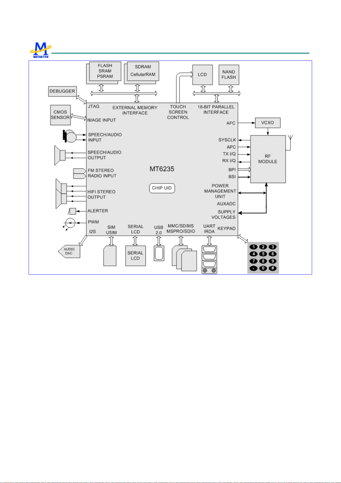
Typical application diagram is shown in Figure 1.
Platform
MT6235 is capable of running the ARM926EJ-S
TM
RISC
processor at up to 208 MHz, thus providing fast data
processing capabilities. In addition to the high clock
frequency, separate CODE and DATA caches are also
included to further improve the overall system efficiency.
For large amounts of data transfer, high performance DMA
(Direct Memory Access) with hardware flow control is
implemented, which greatly enhances the data movement
speed while reducing MCU processing load.
Targeted as a high performance platform for mobile
applications, hardware flash content protection is also
provided to prevent unauthorized porting of the software
load to protect the manufacturer’s development
investment.
Memory
To provide the greatest capacity for expansion and
maximum bandwidth for data intensive applications such
as multimedia features, MT6235 supports up to 4 external
state-of-the-art devices through its 8/16-bit host interface.
High performance devices such as Mobile SDRAM and
Cellular RAM are supported for maximum bandwidth.
Traditional devices such as burst/page mode flash, page
mode SRAM, and Pseudo SRAM are also supported. For
greatest compatibility, the memory interface can also be
used to connect to legacy devices such as Color/Parallel
LCD, and multi-media companion chips are all supported
through this interface. To minimize power consumption
and ensure low noise, this interface is designed for flexible
I/O voltage and allows lowering of the supply voltage
down to 1.8V. The driving strength is configurable for
signal integrity adjustment.
Multi-media
The MT6235 multi-media subsystem provides a
connection to a CMOS image sensor and supports a
resolution up to 2.0 Mpixels. With its high performance
application platform, MT6235 allows efficient processing
of image and video data.
In addition to image and video features, MT6235 utilizes
high resolution DAC, digital audio, and audio synthesis
technology to provide superior audio features for all future
multi-media needs.
Connectivity and Storage
To take advantage of its incredible multimedia strengths,
MT6235 incorporates myriads of advanced connectivity
and storage options for data storage and communication.
MT6235 supports UART, Fast IrDA, USB 2.0, SDIO,
Bluetooth, Touch Screen Controller, WIFI Interface, and
MMC/SD/MS/MS Pro storage systems. These interfaces
provide MT6235 users with the highest degree of
flexibility in implementing solutions suitable for the
targeted application.
To achieve a complete user interface, MT6235 also brings
together all the necessary peripheral blocks for a
multi-media GSM/GPRS/EDGE phone. The peripheral
blocks include the Keypad Scanner with the capability to
detect multiple key presses, SIM Controller, Alerter, Real
Time Clock, PWM, Serial LCD Controller, and General
Purpose Programmable I/Os.
Furthermore, to provide much better configurability and
bandwidth for multi-media products, an additional 18-bit
parallel interface is incorporated. This interface enables
connection to LCD panels as well as NAND flash devices
for additional multi-media data storage.
Audio
6/599 MediaTek Inc. Confidential

MT6235 GSM/GPRS Baseband Processor Data Sheet Revision 1.02
Using a highly integrated mixed-signal Audio Front-End,
the MT6235 architecture allows for easy audio interfacing
with direct connection to the audio transducers. The
audio interface integrates D/A and A/D Converters for
Voice band, as well as high resolution Stereo D/A
Converters for Audio band. In addition, MT6235 also
provides Stereo Input and Analog MUX.
MT6235 supports AMR codec to adaptively optimize
speech and audio quality. Moreover, HE-AAC codec is
implemented to deliver CD-quality audio at low bit rates.
On the whole, MT6235’s audio features provide a rich
solution for multi-media applications.
Radio
MT6235 integrates a mixed-signal baseband front-end in
order to provide a well-organized radio interface with
flexibility for efficient customization. The front-end
contains gain and offset calibration mechanisms, and filters
with programmable coefficients for comprehensive
compatibility control on RF modules. This approach
allows the usage of a high resolution D/A Converter for
controlling VCXO or crystal, reducing the need for an
expensive TCVCXO. MT6235 achieves great MODEM
performance by utilizing a 14-bit high resolution A/D
Converter in the RF downlink path. Furthermore, to
reduce the need for extra external current-driving
component, the driving strength of some BPI outputs is
designed to be configurable.
advanced low leakage CMOS process, hence providing an
overall ultra low leakage solution.
Package
The MT6235 device is offered in a 13mm×13mm, 362-ball,
0.5 mm pitch, TFBGA package.
Debug Function
The JTAG interface enables in-circuit debugging of the
software program with the ARM926EJ-S core. With this
standardized debugging interface, MT6235 provides
developers with a wide set of options in choosing ARM
development kits from different third party vendors.
Power Management
The MT6235 offers various low-power features to help
reduce system power consumption. These features
include a Pause Mode of 32 KHz clocking in Standby State,
Power Down Mode for individual peripherals, and
Processor Sleep Mode. MT6235 is also fabricated in an
7/599 MediaTek Inc. Confidential
MT6235 GSM/GPRS Baseband Processor Data Sheet Revision 1.02
Figure 1 Typical application of MT6235
8/599 MediaTek Inc. Confidential

MT6235 GSM/GPRS Baseband Processor Data Sheet Revision 1.02
Platform Features
General
z Integrated voice-band, audio-band and base-band
analog front ends
z TFBGA 13mm×13mm, 362-ball, 0.5 mm pitch
package
MCU Subsystem
z ARM926EJ-S 32-bit RISC processor
z High performance multi-layer AMBA bus
z Java hardware acceleration for fast Java-based
games and applets
z Operating frequency: 26/52/104/208 MHz
z Dedicated DMA bus
z 14 DMA channels
z 512K bits on-chip SRAM
z 384K bits Instruction-TCM
z 640K bits Data-TCM
z 128K bits Instruction-Cache
z 128K bits Data-Cache
z On-chip boot ROM for Factory Flash
Programming
z Supports Flash and SRAM/PSRAM with page
mode or burst mode
z Industry standard Parallel LCD interface
z Supports multi-media companion chips with 8/16
bits data width
z Flexible I/O voltage of 1.8V ~ 2.8V for memory
interface
z Configurable driving strength for memory
interface
User Interfaces
z 8-row × 8-column keypad controller with
hardware scanner
z Supports multiple key presses for gaming
z SIM/USIM controller with hardware T=0/T=1
protocol control
z Real Time Clock (RTC) operating with a separate
power supply
z General Purpose I/Os (GPIOs)
z 4 sets of Pulse Width Modulation (PWM) output
z Alerter output with Enhanced PWM or PDM
z 8 external interrupt lines
z Watchdog timer for system crash recovery
z 3 sets of General Purpose Timer
z Circuit Switch Data coprocessor
z Division coprocessor
z PPP Framer coprocessor
External Memory Interface
z Supports up to 4 external memory devices
z Supports 8-bit or 16-bit memory components with
maximum size of up to 128M Bytes each
z Supports Mobile SDRAM and Cellular RAM
9/599 MediaTek Inc. Confidential
Security
z Supports security key and 126 bit chip unique ID
Connectivity
z 3 UARTs with hardware flow control and speeds
z IrDA modulator/demodulator with hardware
z USB 2.0 capability
z Multi Media Card, Secure Digital Memory Card,
up to 921600 bps
framer. Supports SIR/MIR/FIR operating speeds.
Memory Stick, Memory Stick Pro host controller
with flexible I/O voltage power

MT6235 GSM/GPRS Baseband Processor Data Sheet Revision 1.02
z Supports SDIO interface for SDIO peripherals as
well as WIFI connectivity
z DAI/PCM and I2S interface for Audio application
Power Management
z Power Down Mode for analog and digital circuits
z Processor Sleep Mode
z Pause Mode of 32 KHz clocking in Standby State
z 4-channel Auxiliary 10-bit A/D Converter for
charger and battery monitoring and photo sensing
Test and Debug
z Built-in digital and analog loop back modes for
both Audio and Baseband Front-End
z DAI port complying with GSM Rec.11.10
z JTAG port for debugging embedded MCU
10/599 MediaTek Inc. Confidential

MT6235 GSM/GPRS Baseband Processor Data Sheet Revision 1.02
1.1 MODEM Features
Radio Interface and Baseband Front End
z GMSK modulator with analog I and Q channel
outputs
z 10-bit D/A Converter for uplink baseband I and Q
signals
z 14-bit high resolution A/D Converter for downlink
baseband I and Q signals
z Calibration mechanism of offset and gain
mismatch for baseband A/D Converter and D/A
Converter
z 10-bit D/A Converter for Automatic Power
Control
z 13-bit high resolution D/A Converter for
Automatic Frequency Control
z Programmable Radio RX filter
z 2 channels Baseband Serial Interface (BSI) with
3-wire control
z Bi-directional BSI interface. RF chip register
read access with 3-wire or 4-wire interface.
z 10-Pin Baseband Parallel Interface (BPI) with
programmable driving strength
z GSM/GPRS quad vocoders for adaptive multirate
(AMR), enhanced full rate (EFR), full rate (FR)
and half rate (HR)
z GSM channel coding, equalization and A5/1, A5/2
and A5/3 ciphering
z GPRS GEA1, GEA2 and GEA3 ciphering
z Programmable GSM/GPRS/EDGE modem
z Packet Switched Data with CS1/CS2/CS3/CS4
coding schemes
z GSM Circuit Switch Data
z GPRS/EDGE Class 12
Voice Interface and Voice Front End
z Two microphone inputs sharing one low noise
amplifier with programmable gain and automatic
gain control (AGC) mechanisms
z Voice power amplifier with programmable gain
nd
order Sigma-Delta A/D Converter for voice
z 2
uplink path
z D/A Converter for voice downlink path
z Supports half-duplex hands-free operation
z Multi-band support
Voice and Modem CODEC
z Dial tone generation
z Voice memo
z Noise reduction
z Echo suppression
z Advanced sidetone Oscillation Reduction
z Digital sidetone generator with programmable
gain
z Two programmable acoustic compensation filters
11/599 MediaTek Inc. Confidential
z Compliant with GSM 03.50

MT6235 GSM/GPRS Baseband Processor Data Sheet Revision 1.02
1.2 Multi-Media Features
LCD/NAND Flash Interface
z Dedicated Parallel Interface supports 3 external
devices with 8-/16-bit NAND flash interface,
8-/9-/16-/18-bit Parallel interface, and Serial
interface for LCM
z Built-in NAND Flash Controller with 1-bit ECC
for mass storage
LCD Controller
z Supports simultaneous connection to up to 3
parallel LCD and 2 serial LCD modules
z Supports LCM format: RGB332, RGB444,
RGB565, RGB666, RGB888
z Supports LCD module with maximum resolution
up to 800x600 at 24bpp
z Per pixel alpha channel
z True color engine
z Supports hardware display rotation
z Capable of combining display memories with up to
6 blending layers
Image Signal Processor
z 8 bit YUV format image input
z Capable of processing image of size up to 2.0 M
pixels
z Horizontal scaling in averaging method
z Vertical scaling in bilinear method
z YUV and RGB color space conversion
z Boundary padding
2D Accelerator
z Supports 32-bpp ARGB8888, 24-bpp RGB888,
16-bpp RGB565, and 8-bpp index color modes
z Supports SVG Tiny
z Rectangle gradient fill
z BitBlt: multi-BitBlt with 7 rotation, 16 binary ROP
z Alpha blending with 7 rotation
z Line drawing: normal line, dotted line,
anti-aliasing
z Circle drawing
z Bezier curve drawing
z Triangle flat fill
z Font caching: normal font, italic font
z Command queue with max depth of 2047
Audio CODEC
z Supports HE-AAC codec decode
z Supports AAC codec decode
z IEEE Std 1180-1990 IDCT standards compliance
z Supports progressive image processing to
minimize storage space requirement
z Supports reload-able DMA for VLD stream
Image Data Processing
z Supports Digital Zoom
z Supports RGB888/565, YUV444 image
processing
z High throughput hardware scaler. Capable of
tailoring an image to an arbitrary size.
12/599 MediaTek Inc. Confidential
z Wavetable synthesis with up to 64 tones
z Advanced wavetable synthesizer capable of
generating simulated stereo
z Wavetable including GM full set of 128
instruments and 47 sets of percussions
z PCM Playback and Record
z Digital Audio Playback
Audio Interface and Audio Front End
z Supports I2S interface

MT6235 GSM/GPRS Baseband Processor Data Sheet Revision 1.02
z High resolution D/A Converters for Stereo Audio
playback
z Analog multiplexer for stereo audio
z Stereo to mono conversion
z Stereo analog input for stereo audio source
1.3 General Description
Figure 2 depicts the block diagram of MT6235. Based on a dual-processor architecture, MT6235 integrates both an
ARM926EJ-S core and a digital signal processor core. ARM926EJ-S is the main processor responsible for running
high-level GSM/GPRS protocol software as well as multi-media applications. The digital signal processor manages the
low-level MODEM as well as advanced audio functions. Except for a few mixed-signal circuitries, the other building
blocks in MT6235 are connected to either the microcontroller or the digital signal processor.
MT6235consists of the following subsystems:
z Microcontroller Unit (MCU) Subsystem: includes an ARM926EJ-S RISC processor and its accompanying
memory management and interrupt handling logics;
z Digital Signal Processor (DSP) Subsystem: includes a DSP and its accompanying memory, memory controller, and
interrupt controller;
z MCU/DSP Interface: the junction at which the MCU and the DSP exchange hardware and software information;
z Microcontroller Peripherals: includes all user interface modules and RF control interface modules;
z Microcontroller Coprocessors: runs computing-intensive processes in place of the Microcontroller;
z DSP Peripherals: hardware accelerators for GSM/GPRS/EDGE channel codec;
z Multi-media Subsystem: integrates several advanced accelerators to support multi-media applications;
z Voice Front End: the data path for converting analog speech to and from digital speech;
z Audio Front End: the data path for converting stereo audio from an audio source;
z Baseband Front End: the data path for converting a digital signal to and from an analog signal from the RF
modules;
z Timing Generator: generates the control signals related to the TDMA frame timing; and,
z Power, Reset and Clock Subsystem: manages the power, reset, and clock distribution inside MT6235.
Details of the individual subsystems and blocks are described in the following chapters.
13/599 MediaTek Inc. Confidential
MT6235 GSM/GPRS Baseband Processor Data Sheet Revision 1.02
Figure 2 MT6235 block diagram.
14/599 MediaTek Inc. Confidential

MT6235 GSM/GPRS Baseband Processor Data Sheet Revision 1.02
2 Product Description
2.1 Pin Outs
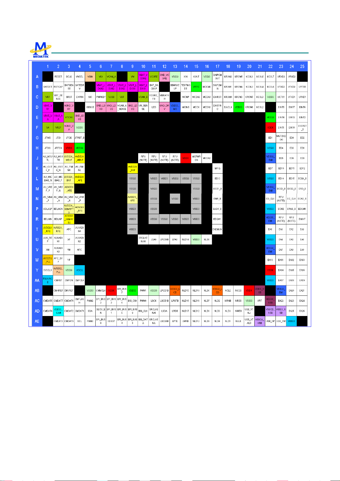
One type of package for this product, TFBGA 13mm*13mm, 362-ball, 0.5 mm pitch package, is offered.
Pin-outs and the top view are illustrated in Figure 3 for this package. Outline and dimension of package is illustrated in
Figure 4, while the definition of package is shown in Table 1.
15/599 MediaTek Inc. Confidential
MT6235 GSM/GPRS Baseband Processor Data Sheet Revision 1.02
Figure 3 Top view of MT6235 TFBGA 13mm*13mm, 362-ball, 0.5 mm pitch package
Notes: RFU is reserved for future use and leave as NC in normal operation.
16/599 MediaTek Inc. Confidential

MT6235 GSM/GPRS Baseband Processor Data Sheet Revision 1.02
Figure 4 Outlines and dimension of TFBGA 13mm*13mm, 362-ball, 0.5 mm pitch package
Body Size Ball Count Ball Pitch Ball Dia. Package Thk. Stand Off Substrate Thk.
D E N e b A (MAX) A1(NOM) C
13 13 362 0.5 0.3 1.2 0.21 0.36
Table 1 Definition of TFBGA 13mm*13mm, 362-ball, 0.5 mm pitch package (Unit: mm)
17/599 MediaTek Inc. Confidential

MT6235 GSM/GPRS Baseband Processor Data Sheet Revision 1.02
2.2 Top Marking Definition
MT6235A
DDDD-###
LLLLL
S
MT6235A: Part No.
DDDD: Date Code
###: Subcontractor Code
LLLLL: U1 Die Lot No.
S: Special Code
18/599 MediaTek Inc. Confidential
MT6235 GSM/GPRS Baseband Processor Data Sheet Revision 1.02
2.3 DC Characteristics
2.3.1 Absolute Maximum Ratings
Prolonged exposure to absolute maximum ratings may reduce device reliability. Functional operation at these maximum
ratings is not implied.
Item Symbol Min Max Unit
IO power supply VDD33 -0.3 VDD33+0.3 V
I/O input voltage VDD33 -0.3 VDD33+0.3 V
Operating temperature Topr -20 80 Celsius
Storage temperature Tstg -55 125 Celsius
19/599 MediaTek Inc. Confidential

MT6235 GSM/GPRS Baseband Processor Data Sheet Revision 1.02
2.4 Pin Description
Ball
Name Dir
13X13
Description
Mode0 Mode1 Mode2 Mode3
PU/PDRese
t
G4 JTRST_B I JTAG test port reset input PD PD
G3 JTCK I JTAG test port clock input PU PU
G2 JTDI I JTAG test port data input PU PU
G1 JTMS I JTAG test port mode switch PU PU
H1 JTDO IO JTAG test port data output
H2 JRTCK IO JTAG test port returned clock output
AE6 BPI_BUS0 IO RF hard-wire control bus 0
AD7 BPI_BUS1 IO RF hard-wire control bus 1
JTAG Port
RF Parallel Control Unit
AC7 BPI_BUS2 IO RF hard-wire control bus 2
AC6 BPI_BUS3 IO RF hard-wire control bus 3
AE8 BPI_BUS4 IO RF hard-wire control bus 4
AD8 BPI_BUS5 IO RF hard-wire control bus 5
AC8 BPI_BUS6 IO RF hard-wire control bus 6
AB8 BPI_BUS7 IO RF hard-wire control bus 7
20/599 MediaTek Inc. Confidential
GPIO19
GPIO20
GPIO21
BPI_BUS3 PU/PDPD
BPI_BUS6 PU/PDPD
BPI_BUS7 PU/PDPD

MT6235 GSM/GPRS Baseband Processor Data Sheet Revision 1.02
AE9 BPI_BUS8 IO RF hard-wire control bus 8
AD9 BPI_BUS9 IO RF hard-wire control bus 9
AC9 BSI_CS0 IO RF 3-wire interface chip select 0
AE10 BSI_DATA IO RF 3-wire interface data output
AD10 BSI_CLK IO RF 3-wire interface clock output
AC10 PWM0 IO Pulse width modulated signal 0
AB10 PWM1 IO Pulse width modulated signal 1
RF Serial Control Unit
PWM Interface
GPIO22
GPIO23
GPIO39
GPIO40
BPI_BUS8 PU/PDPD
BPI_BUS9 BSI_CS1 PU/PDPD
PWM0 PU/PDPD
PWM1 BSI_RFIN PU/PDPD
AC5 PWM2 IO Pulse width modulated signal 2
AE5 PWM3 IO Pulse width modulated signal 3
AE4 SCL IO
AD5 SDA IO
AC11 LSCK IO Serial display interface data output
U11 LSA0 IO Serial display interface address output
Camera Control Interface
Serial LCD/PM IC Interface
GPIO17
GPIO18
GPIO15
GPIO16
GPIO24
GPIO25
PWM2 D2_TID5 PU/PDPD
PWM3 D2_TID6 PU/PDPD
SCL D2_TID3 PU/PDPU
SDA D2_TID4 PU/PDPU
LSCK DSP_GPO2 IRQ0 PU/PDPD
LSA0 DSP_GPO3 IRQ1 PU/PDPD
21/599 MediaTek Inc. Confidential

MT6235 GSM/GPRS Baseband Processor Data Sheet Revision 1.02
AD12 LSDA IO Serial display interface clock output
AE12 LSCE0B IO Serial display interface chip select 0
output
LSCE1B IO
AC12
AB12 LPCE1B IO
U12 LPCE0B IO
AE13 LPTE IO
AC13 LRSTB IO Parallel display interface Reset Signal
AD13 LRDB IO Parallel display interface Read Strobe
U13 LPA0 IO
AE14 LWRB IO Parallel display interface Write Strobe
AD14 NLD17 IO Parallel LCD/NAND-Flash Data 17
AC14 NLD16 IO Parallel LCD/NAND-Flash Data 16
AB14 NLD15 IO Parallel LCD/NAND-Flash Data 15 PD
U14 NLD14 IO Parallel LCD/NAND-Flash Data 14 PD
AE15 NDL13 IO Parallel LCD/NAND-Flash Data 13 PD
AD15 NLD12 IO Parallel LCD/NAND-Flash Data 12 PD
AC15 NLD11 IO Parallel LCD/NAND-Flash Data 11 PD
AB15 NLD10 IO Parallel LCD/NAND-Flash Data 10 PD
AE16 NLD9 IO Parallel LCD/NAND-Flash Data 9 PD
AD16 NLD8 IO Parallel LCD/NAND-Flash Data 8 PD
AC16 NLD7 IO Parallel LCD/NAND-Flash Data 7 PD
AB16 NLD6 IO Parallel LCD/NAND-Flash Data 6 PD
U16 NLD5 IO Parallel LCD/NAND-Flash Data 5 PD
AE17 NLD4 IO Parallel LCD/NAND-Flash Data 4 PD
AD17 NLD3 IO Parallel LCD/NAND-Flash Data 3 PD
AC17 NLD2 IO Parallel LCD/NAND-Flash Data 2 PD
AE18 NLD1 IO Parallel LCD/NAND-Flash Data 1 PD
AD18 NLD0 IO Parallel LCD/NAND-Flash Data 0 PD
AC18 NRNB IO NAND-Flash Read/Busy Flag GPIO33
AB18 NCLE IO NAND-Flash Command Latch Signal GPIO34
AE19 NALE IO NAND-Flash Address Latch Signal GPIO35
AD19 NWEB IO NAND-Flash Write Strobe GPIO36
AC19 NREB IO NAND-Flash Read Strobe GPIO37
Serial display interface chip select 1
output
Parallel LCD/NAND-Flash Interface
Parallel display interface chip select 1
output
Parallel display interface chip select 0
output
Parallel display interface address
output
GPIO26
GPIO27
GPIO28
GPIO29
GPIO30
GPIO31
GPIO32
LSDA CLKM1 TDTIRQ PU/PDPD
LSCE0B CLKM2 TCTIRQ2 PU/PDPU
LSCE1B LPCE2B TCTIRQ1
LPCE1B NCE1B TEVTVAL
LPTE
NLD17
NLD16
NRNB
NCLE
NALE
NWEB
NREB
PU/
PD
PU/
PD
PU/
PD
PU/
PD
PU/
PD
PU/
PD
PU/
PD
PU/
PD
PU/
PD
PU/
PD
PU
PU
PD
PD
PD
PU
22/599 MediaTek Inc. Confidential

MT6235 GSM/GPRS Baseband Processor Data Sheet Revision 1.02
AB19 NCEB IO NAND-Flash Chip select output GPIO38
F25 SYSRST_B I System reset input active low PU PU
G23 WATCHDOG IO Watchdog reset output
U10 SRCLKENAN IO
AE11 SRCLKENA IO
AD11 SRCLKENAI IO External TCXO enable input
B14 TESTMODE I TESTMODE enable input PD PD
Y4 VCCQ I
AA1 FSOURCE I
AD6 SECU_EN I
AE7 XBOOT I PD PD
A22 KCOL7 IO Keypad column 7
B22 KCOL6 IO Keypad column 6
A21 KCOL5 IO Keypad column 5
B21 KCOL4 IO Keypad column 4
C21 KCOL3 IO Keypad column 3
D21 KCOL2 IO Keypad column 2
A20 KCOL1 IO Keypad column 1
B20 KCOL0 IO Keypad column 0
C20 KROW7 IO Keypad row 7
D20 KROW6 IO Keypad row 6
A19 KROW5 IO Keypad row 5
B19 KROW4 IO Keypad row 4
C19 KROW3 IO Keypad row 3
A18 KROW2 IO Keypad row 2
B18 KROW1 IO Keypad row 1
C18 KROW0 IO Keypad row 0
F24 EINT0 IO External interrupt 0 PU PU
F23 EINT1 IO External interrupt 1 PU PU
E25 EINT2 IO External interrupt 2 PU PU
E24 EINT3 IO External interrupt 3
E23 EINT4 IO External interrupt 4
D23 EINT5 IO External interrupt 5
D25 EINT6 IO External interrupt 6
D24 EINT7 IO External interrupt 7
Miscellaneous
External TCXO enable output active
low
External TCXO enable output active
high
Keypad Interface
External Interrupt Interface
GPIO42
GPIO41
GPIO43
GPIO55
GPIO56
GPIO57
GPIO58
GPIO44
GPIO45
GPIO46
GPIO47
GPIO48
NCE0B
SRCLKEN
AN
SRCLKEN
A
SRCLKEN
AI
KCOL7 IRDA_PDN
KCOL6
PU PU
PU PU
PU PU
PU PU
PU PU
PU PU
KROW7 CLKM4
KROW6
EINT3
EINT4 DRF_EN CLKM3
EINT5 EDICK
EINT6 EDIWS
EINT7 EDIDAT
DRF_DAT
A
IRQ2
PU/
PD
PU/
PD
PU/
PD
PU/
PD
PU/
PD
PU/
PD
PU/
PD
PU/
PD
PU/
PD
PU/
PD
PU/
PD
PU/
PD
PU/
PD
PD
PU
PU
PD
PD
PU
PU
PU
PU
PU
23/599 MediaTek Inc. Confidential

MT6235 GSM/GPRS Baseband Processor Data Sheet Revision 1.02
K17 MFIQ IO Interrupt to MCU
G24 ED0 IO External memory data bus 0
G22 ED1 IO External memory data bus 1
G25 ED2 IO External memory data bus 2
H24 ED3 IO External memory data bus 3
H23 ED4 IO External memory data bus 4
J23 ED5 IO External memory data bus 5
J24 ED6 IO External memory data bus 6
K22 ED7 IO External memory data bus 7
H25 ED8 IO External memory data bus 8
J25 ED9 IO External memory data bus 9
K23 ED10 IO External memory data bus 10
K24 ED11 IO External memory data bus 11
K25 ED12 IO External memory data bus 12
L17 ED13 IO External memory data bus 13
L23 ED14 IO External memory data bus 14
L24 ED15 IO External memory data bus 15
M25 ERD_B IO External memory read strobe
N17 EWR_B IO External memory write strobe
L25 ECS0_B IO External memory chip select 0
M17 ECS1_B IO External memory chip select 1
M23 ECS2_B IO External memory chip select 2
M24 ECS3_B IO External memory chip select 3
R25 EWAIT IO
N25 ECAS_B IO MobileRAM column address
P24 ERAS_B IO MobileRAM row address
P23 ECKE IO MobileRAM clock enable
N22 ED_CLK O MobileRAM clock
T17 EADMUX IO GPIO65
R17 EDQM1 IO
P25 EDQM0 IO
P17 EADV_B O
N24 EC_CLK O
T23 EA0 IO External memory address bus 0
T22 EA1 IO External memory address bus 1
T24 EA2 IO External memory address bus 2
T25 EA3 IO External memory address bus 3
U23 EA4 IO External memory address bus 4
U24 EA5 IO External memory address bus 5
U25 EA6 IO External memory address bus 6
V23 EA7 IO External memory address bus 7
V24 EA8 IO External memory address bus 8
V25 EA9 IO External memory address bus 9
W22 EA10 IO External memory address bus 10
External Memory Interface
Flash, PSRAM and CellularRAM data
ready
Flash, PSRAM and CellularRAM
address valid
Flash, PSRAM and CellularRAM
clock
GPIO66
PD
:nFIQ CLKM7
EADMUX
CLKM6
PU/
PD
PU/
PD
PU
24/599 MediaTek Inc. Confidential

MT6235 GSM/GPRS Baseband Processor Data Sheet Revision 1.02
W23 EA11 IO External memory address bus 11
W24 EA12 IO External memory address bus 12
W25 EA13 IO External memory address bus 13
Y23 EA14 IO External memory address bus 14
Y24 EA15 IO External memory address bus 15
Y25 EA16 IO External memory address bus 16
AA23 EA17 IO External memory address bus 17
AA24 EA18 IO External memory address bus 18
AA25 EA19 IO External memory address bus 19
AB24 EA20 IO External memory address bus 20
AB25 EA21 IO External memory address bus 21
AC23 EA22 IO External memory address bus 22
AC24 EA23 IO External memory address bus 23
AC25 EA24 IO External memory address bus 24
AD24 EA25 IO External memory address bus 25
AD25 EA26 IO External memory address bus 26 GPIO64
AD20 USB_XTALI IO
AE20 USB_XTALO IO
AE21 VSSCA_USB IO
AD22 VSSCD_USB IO
AC21 VRT IO
AD23 VSS33_USB IO
AE22 USB_DP IO USB D+ Input/Output
AE23 USB_DM IO USB D- Input/Output
B16 MCCM0 IO SD Command/MS Bus State Output
C16 MCDA0 IO
D16 MCDA1 IO SD Serial Data IO 1
J16 MCDA2 IO SD Serial Data IO 2
C15 MCDA3 IO SD Serial Data IO 3
D15 MCCK IO
J15 MCPWRON IO SD Power On Control Output
C14 MCWP IO SD Write Protect Input
D14 MCINS IO SD Card Detect Input
C25 URXD1 IO UART 1 receive data PU
C24 UTXD1 IO UART 1 transmit data
C23 UCTS1 IO UART 1 clear to send GPIO49
B25 URTS1 IO UART 1 request to send GPIO50
USB Interface
Memory Card Interface
SD Serial Data IO 0/MS Serial Data
IO
SD Serial Clock/MS Serial Clock
Output
UART/IrDA I nterface
GPIO67
GPIO68
GPIO69
GPIO70
GPIO71
GPIO72
GPIO73
GPIO74
GPIO75
EA26
MC0CM0
MC0DA0
MC0DA1
MC0DA2 TDMA_FS
MC0DA3
MC0CK
MC0PWR
ON
MC0WP CLKM9
MC0INS
UCTS1
URTS1
CLKM5
TDMA_CK PU/
TDMA_D1 PU/
TDMA_D0 PU/
CLKM8
UCTS2
URTS2
PU/
PD
PD
PD
PD
PU/
PD
PU/
PD
PU/
PD
PU/
PD
PU/
PD
PU/
PD
PU/
PD
PU/
PU
PU
PU
PU
PU
PU
PU
PU
PU
PU
25/599 MediaTek Inc. Confidential

MT6235 GSM/GPRS Baseband Processor Data Sheet Revision 1.02
PD
A24 URXD2 IO UART 2 receive data
B24 UTXD2 IO UART 2 transmit data
A23 URXD3 IO UART 3 receive data
B23 UTXD3 IO UART 3 transmit data
D18 DAICLK IO DAI clock output
A17 DAIPCMOUT IO DAI pcm data out
B17 DAIPCMIN IO DAI pcm data input
C17 DAIRST IO DAI reset signal input
D17 DAISYNC IO
AA2 CMRST IO CMOS sensor reset signal output
AA3 CMPDN IO CMOS sensor power down control
AB3 CMVREF IO Sensor vertical reference signal input
AB2 CMHREF IO
AA4 CMPCLK IO CMOS sensor pixel clock input
AB6 CMMCLK IO CMOS sensor master clock output
AC2 CMDAT7 IO CMOS sensor data input 7
AC3 CMDAT6 IO CMOS sensor data input 6
AC1 CMDAT5 IO CMOS sensor data input 5
AD1 CMDAT4 IO CMOS sensor data input 4
AE2 CMDAT3 IO CMOS sensor data input 3
AD3 CMDAT2 IO CMOS sensor data input 2
AD4 CMDAT1 IO CMOS sensor data input 1
AE3 CMDAT0 IO CMOS sensor data input 0
AC4 CMFLASH IO
J1 AU_MOUTL O Audio analog output left channel
Digital Audio Interface
DAI frame synchronization signal
output
CMOS Sensor Interf ace
Sensor horizontal reference signal
input
Analog Interface
GPIO51
GPIO52
GPIO53
GPIO54
GPIO59
GPIO60
GPIO61
GPIO62
GPIO63
GPIO0
GPIO1
GPIO2
GPIO3
GPIO4
GPIO5
GPIO6
GPIO7
GPIO8
GPIO9
GPIO10
GPIO11
GPIO12
GPIO13
GPIO14
URXD2 UCTS3
UTXD2 URTS3
URXD3
UTXD3
DAICLK
DAIPCMO
UT
DAIPCMI
N
DAIRST
DAISYNC
CMRST CLKM0
CMPDN
CMVREF TBTXEN D1_TID0
CMHREF TBTXFS
CMPCLK TBRXEN D1_TID1
CMMCLK TBRXFS
CMDAT7 D1ICK
CMDAT6
CMDAT5 D1IMS
CMDAT4 D2ICK
CMDAT3 D2ID
CMDAT2 D2IMS
CMDAT1 D2_TID0
CMDAT0 D2_TID1
CMFLASH D2_TID2
IRDA_RX
D
IRDA_TX
D
D1ID
DSP_GPO0 PU/
DSP_GPO1 PU/
PU/
PD
PU/
PD
PU/
PD
PU/
PD
PU/
PD
PU/
PD
PU/
PD
PU/
PD
PU/
PD
PD
PD
PU/
PD
PU/
PD
PU/
PD
PU/
PD
PU/
PD
PU/
PD
PU/
PD
PU/
PD
PU/
PD
PU/
PD
PU/
PD
PU/
PD
PU/
PD
PU
PU
PU
PU
PD
PD
PD
PD
PD
PD
PD
PD
PD
PD
PD
PD
PD
PD
PD
PD
PD
PD
PD
PD
26/599 MediaTek Inc. Confidential

MT6235 GSM/GPRS Baseband Processor Data Sheet Revision 1.02
J2 AU_MOUTR O Audio analog output right channel
K4 AU_FMINL I FM radio analog input left channel
K3 AU_FMINR I FM radio analog input right channel
K2 AU_OUT0_N O Earphone 0 amplifier output (-)
K1 AU_OUT0_P O Earphone 0 amplifier output (+)
L2
AU_MICBIAS
_P
L1
AU_MICBIAS
_N
M2 AU_VREF_N O Audio reference voltage (-)
M1 AU_VREF_P O Audio reference voltage (+)
N1 AU_VIN0_P I Microphone 0 amplifier input (+)
N2 AU_VIN0_N I Microphone 0 amplifier input (-)
N3 AU_VIN1_N I Microphone 1 amplifier input (-)
N4 AU_VIN1_P I Microphone 1 amplifier input (+)
P1 BDLAQP I
P2 BDLAQN I
R1 BDLAIN I
R2 BDLAIP I
T3 APC I Automatic power control DAC output
T4 AUXADIN0 I Auxiliary ADC input 0
U2 AUXADIN1 I Auxiliary ADC input 1
U4 AUXADIN2 I Auxiliary ADC input 2
V2 AUXADIN3 I Auxiliary ADC input 3
U1 AUX_REF I Auxiliary ADC reference voltage input
U3 XP I
V1 XM I
W3 YP I
V3 YM I
V4 AFC O
W2 AFC_BYP O Automatic frequency control DAC
B1 BATDET I
C2 VRF_SENSE I
C1 VRF I
E3 VTCXO I
F2 VREF I
C12 VIBRATOR O
D11 LED O
A11 VCORE I
C11 VCORE_FB I
B11
BAT_BACKU
P
F1 VA
A9 VM I
D10 VM_SENSE I
O Microphone bias supply (+)
O Microphone bias supply (-)
Quadrature input (Q+) baseband codec
downlink
Quadrature input (Q-) baseband codec
downlink
In-phase input (I+) baseband codec
downlink
In-phase input (I-) baseband codec
downlink
Automatic frequency control DAC
output
bypass capacitance
I
27/599 MediaTek Inc. Confidential

MT6235 GSM/GPRS Baseband Processor Data Sheet Revision 1.02
C10 VCAM_D II
D8
VCAM_A_SE
NSE
A7 VCAM_A
C8 VBT I
A6 VIO I
C7 VUSB I
A5 VSIM I
C5 SIO IO
C6 PWRKEY I
D5 ISENSE I
A4 VMSEL I
B4 GATEDRV I
C4 CHRIN I
A3 SCLK I
B3 BATSENSE I
C3 SRST O
A2 RESET I
B2 RSTCAP IO
Y1 SYSCLK I 13MHz or 26MHz system clock input
A14 XIN I 32.768 KHz crystal input
A15 XOUT O 32.768 KHz crystal output
B13 BBWAKEUP IO Baseband power on/off control
H3 VDDK Supply voltage of internal logic
AB7 VDDK Supply voltage of internal logic
AB20 VDDK Supply voltage of internal logic
Y22 VDDK Supply voltage of internal logic
F22 VDDK Supply voltage of internal logic
J14 VDDK Supply voltage of internal logic
AB23 VDD33_EMI
V22 VDD33_EMI
R22 VDD33_EMI
M22 VDD33_EMI
J22 VDD33_EMI
AD2 VDD33_CAM
AB13 VDD33_LCD
AB17 VDD33_LCD
AC22 VDD33_USB
AB21 VDDC_USB
D13 VDD33_MC
I
I
VCXO Interface
RTC Interface
Supply V oltages
Supply voltage of memory interface
driver
Supply voltage of memory interface
driver
Supply voltage of memory interface
driver
Supply voltage of memory interface
driver
Supply voltage of memory interface
driver
28/599 MediaTek Inc. Confidential

MT6235 GSM/GPRS Baseband Processor Data Sheet Revision 1.02
H4 VDD33
AB9 VDD33
E22 VDD33
D19 VDD33 Supply voltage of drivers except
F4 VSS33
Y3 VSS33
AB5 VSS33
AB11 VSS33
U15 VSS33
AC20 VSS33
AE24 VSS33
AA22 VSS33
U22 VSS33
P22 VSS33
L22 VSS33
H22 VSS33
C22 VSS33
A16 VSS33
A13 VSS33
L9 VSS33
L11 VSS33
L12 VSS33
L13 VSS33
L14 VSS33
L15 VSS33
Supply voltage of drivers except
memory interface, USB and
MS/MMC/SD
Supply voltage of drivers except
memory interface, USB and
MS/MMC/SD
Supply voltage of drivers except
memory interface, USB and
MS/MMC/SD
memory interface, USB and
MS/MMC/SD
Ground of drivers except memory
interface, USB and MS/MMC/SD
Ground of drivers except memory
interface, USB and MS/MMC/SD
Ground of drivers except memory
interface, USB and MS/MMC/SD
Ground of drivers except memory
interface, USB and MS/MMC/SD
Ground of drivers except memory
interface, USB and MS/MMC/SD
Ground of drivers except memory
interface, USB and MS/MMC/SD
Ground of drivers except memory
interface, USB and MS/MMC/SD
Ground of drivers except memory
interface, USB and MS/MMC/SD
Ground of drivers except memory
interface, USB and MS/MMC/SD
Ground of drivers except memory
interface, USB and MS/MMC/SD
Ground of drivers except memory
interface, USB and MS/MMC/SD
Ground of drivers except memory
interface, USB and MS/MMC/SD
Ground of drivers except memory
interface, USB and MS/MMC/SD
Ground of drivers except memory
interface, USB and MS/MMC/SD
Ground of drivers except memory
interface, USB and MS/MMC/SD
Ground of drivers except memory
interface, USB and MS/MMC/SD
Ground of drivers except memory
interface, USB and MS/MMC/SD
Ground of drivers except memory
interface, USB and MS/MMC/SD
Ground of drivers except memory
interface, USB and MS/MMC/SD
Ground of drivers except memory
interface, USB and MS/MMC/SD
Ground of drivers except memory
interface, USB and MS/MMC/SD
29/599 MediaTek Inc. Confidential

MT6235 GSM/GPRS Baseband Processor Data Sheet Revision 1.02
M9 VSS33
M11 VSS33
M15 VSS33
N11 VSS33
N13 VSS33
N15 VSS33
P9 VSS33
P11 VSS33
P15 VSS33
R9 VSS33
R11 VSS33
R12 VSS33
R13 VSS33
R14 VSS33
R15 VSS33
T9 VSS33
W1 AVCC12_PLL
Y2 AVSS12_PLL
B15 VRTC Supply voltage for Real Time Clock
J4
AVDD28_MB
UF
J3
AVSS28_MBU
F
K9 AVDD28_BUF
L3 AVSS28_BUF GND for voice band transmit section
L4 AVDD28_AFE
M3 AGND28_AFE
N9 AVSS28_AFE GND for voice band receive section
P4 AGND28_RFE
P3
AVSS28_GSM
RFTX
Ground of drivers except memory
interface, USB and MS/MMC/SD
Ground of drivers except memory
interface, USB and MS/MMC/SD
Ground of drivers except memory
interface, USB and MS/MMC/SD
Ground of drivers except memory
interface, USB and MS/MMC/SD
Ground of drivers except memory
interface, USB and MS/MMC/SD
Ground of drivers except memory
interface, USB and MS/MMC/SD
Ground of drivers except memory
interface, USB and MS/MMC/SD
Ground of drivers except memory
interface, USB and MS/MMC/SD
Ground of drivers except memory
interface, USB and MS/MMC/SD
Ground of drivers except memory
interface, USB and MS/MMC/SD
Ground of drivers except memory
interface, USB and MS/MMC/SD
Ground of drivers except memory
interface, USB and MS/MMC/SD
Ground of drivers except memory
interface, USB and MS/MMC/SD
Ground of drivers except memory
interface, USB and MS/MMC/SD
Ground of drivers except memory
interface, USB and MS/MMC/SD
Ground of drivers except memory
interface, USB and MS/MMC/SD
Analog Supplies
Supply Voltage for Audio band section
GND for Audio band section
Supply voltage for voice band transmit
section
Supply voltage for voice band receive
section
GND reference voltage for voice band
section
GND reference voltage for baseband
section, APC, AFC and AUXADC
GND for baseband transmit section
30/599 MediaTek Inc. Confidential
 Loading...