

MediaTek MT6229, MT6230 Schematics

M
T6229 / MT6230 GSM/GPRS/EDGE Baseband Processor Data Sheet Revision 2.01
GS
M
T6229 / MT6230
M/GPRS/EDGE Baseband
Processor
Data Sheet
Re
vision 2.01
Nov 3, 2006
1
/667 MediaTek Inc. Confidential

M
T6229 / MT6230 GSM/GPRS/EDGE Baseband Processor Data Sheet Revision 2.01
Revision History
R
evision
1.00 Mar 16, 2006 Initial Release
2.00 Sep 12, 2006 Add MT6230 product branch
2.01 Nov 3, 2006 Modify TV-out description on MT6230 product branch
Date Comments
2
/667 MediaTek Inc. Confidential

M
T6229 / MT6230 GSM/GPRS/EDGE Baseband Processor Data Sheet Revision 2.01
TABLE OF CONTENTS
R
evision History...................................................................................................................................... 2
1. System Overview............................................................................................................................... 5
1.
1 Platform Features ....................................................................................................................................................... 8
1.2 MODEM Features.................................................................................................................................................... 10
1.3 Multi-Media Features................................................................................................................................................11
1.4 General Description ................................................................................................................................................. 14
2 Product Descriptions ...................................................................................................................... 16
2.1 Pin Outs.................................................................................................................................................................... 16
2.2 Top Marking Definition ........................................................................................................................................... 19
DC Characteristics............................................................................................................................................................. 19
DC Characteristics............................................................................................................................................................. 20
2.3 Pin Description......................................................................................................................................................... 21
3 Micro-Controller Unit Subsystem ................................................................................................. 35
3.
1 Processor Core ......................................................................................................................................................... 36
3.2 Memory Management .............................................................................................................................................. 36
3.3 Bus System............................................................................................................................................................... 40
3.4 Direct Memory Access............................................................................................................................................. 43
3.5 Interrupt Controller .................................................................................................................................................. 61
3.6 Code Cache Controller ............................................................................................................................................. 77
3.7 MPU......................................................................................................................................................................... 86
3.8 Data Cache ............................................................................................................................................................... 95
3.9 Internal Memory Interface ..................................................................................................................................... 105
3.10 External Memory Interface .................................................................................................................................... 105
4 Microcontroller Peripherals ........................................................................................................ 115
4.
1 Pulse-Width Modulation Outputs............................................................................................................................115
4.2 Alerter .....................................................................................................................................................................118
4.3 SIM Interface ......................................................................................................................................................... 120
4.4 Keypad Scanner ..................................................................................................................................................... 130
4.5 General Purpose Inputs/Outputs ............................................................................................................................ 132
4.6 General Purpose Timer........................................................................................................................................... 148
4.7 UART..................................................................................................................................................................... 151
4.8 IrDA Framer........................................................................................................................................................... 166
4.9 Real Time Clock .................................................................................................................................................... 175
4.10 Auxiliary ADC Unit ............................................................................................................................................... 181
4.11 I2C / SCCB ............................................................................................................................................................ 184
4.12 Cipher Hash Engine (CHE).................................................................................................................................... 189
5 Microcontroller Coprocessors ..................................................................................................... 198
5.
1 Divider ................................................................................................................................................................... 198
5.2 CSD Accelerator .................................................................................................................................................... 200
5.3 FCS Codec ............................................................................................................................................................. 212
5.4 PPP Framer Coprocessor (PFC)................................................................................................................................. 214
6 Multi-Media Subsystem ............................................................................................................... 219
6.
1 LCD Interface ........................................................................................................................................................ 219
6.2 NAND FLASH interface ....................................................................................................................................... 241
6.3 USB OTG Controller ............................................................................................................................................. 258
6.4 Memory Stick and SD Memory Card Controller ................................................................................................... 276
6.5 Graphic Memory Controller................................................................................................................................... 300
6.6 2D acceleration ...................................................................................................................................................... 303
3
/667 MediaTek Inc. Confidential

M
T6229 / MT6230 GSM/GPRS/EDGE Baseband Processor Data Sheet Revision 2.01
6.7 C
6.8 Drop Resize............................................................................................................................................................ 334
6.9 Post Resize ............................................................................................................................................................. 337
6.10 JPEG Decoder ........................................................................................................................................................ 351
6.11 JPEG Encoder ........................................................................................................................................................ 363
6.12 GIF Decoder........................................................................................................................................................... 369
6.13 PNG Decoder......................................................................................................................................................... 380
6.14 Camera Interface .................................................................................................................................................... 391
6.15 Image DMA ........................................................................................................................................................... 444
6.16 Image Engine ......................................................................................................................................................... 475
6.17 MPEG-4/H.263 Video CODEC ............................................................................................................................. 495
6.18 TV Controller ......................................................................................................................................................... 535
6.19 TV encoder............................................................................................................................................................. 541
apture Resize ....................................................................................................................................................... 325
7 Audio Front-End........................................................................................................................... 550
7.
1 General Description ............................................................................................................................................... 550
7.2 Register Definitions ............................................................................................................................................... 553
7.3 Programming Guide ............................................................................................................................................... 557
8 Radio Interface Control ............................................................................................................... 559
8.1 Baseband Serial Interface....................................................................................................................................... 559
8.2 Baseband Parallel Interface.................................................................................................................................... 567
8.3 Automatic Power Control (APC) Unit ................................................................................................................... 571
8.4 Automatic Frequency Control (AFC) Unit ............................................................................................................ 577
8.5 Baseband Serial Ports............................................................................................................................................. 579
9 Baseband Front End..................................................................................................................... 584
9.
1 Downlink Path (RX Path) ...................................................................................................................................... 585
9.2 Uplink Path (TX Path) ........................................................................................................................................... 593
10 Timing Generator ......................................................................................................................... 601
10.1 TDMA timer........................................................................................................................................................... 601
10.2 Slow Clocking Unit................................................................................................................................................ 610
11 Power, Clocks and Reset .............................................................................................................. 613
11.1 B2PSI ..................................................................................................................................................................... 613
11.2 Clocks .................................................................................................................................................................... 615
11.3 Reset Management ................................................................................................................................................. 621
11.4 Software Power Down Control .............................................................................................................................. 625
12 Analog Front-end & Analog Blocks ............................................................................................ 630
12
.1 General Description ............................................................................................................................................... 630
12.2 MCU Register Definitions ..................................................................................................................................... 641
12.3 Programming Guide ............................................................................................................................................... 652
13 Digital Pin Electrical Characteristics.......................................................................................... 663
4
/667 MediaTek Inc. Confidential

M
T6229 / MT6230 GSM/GPRS/EDGE Baseband Processor Data Sheet Revision 2.01
1. System Overview
B
oth MT6229 and MT6230 are feature-rich and extremely
powerful single-chip solutions for high-end mobile phones
with GSM/GPRS and EDGE capability. Based on 32 bit
ARM7EJ-STM RISC processor, MT6229 / MT6230’s
superb processing power along with high bandwidth
architecture and dedicated hardware support provides an
unprecedented platform for high performance EGPRS
Class 12 MODEM and leading-edge multimedia
applications. To sum up, MT6229 / MT6230 both present a
revolutionary platform for multimedia-centric mobile
devices along with an EDGE capable modem.
Flash, page mode SRAM, and Pseudo SRAM are also
supported. For greatest compatibility, the memory interface
can also be used to connect to legacy devices such as
Color/Parallel LCD, and multi-media companion chip are
all supported through this interface. To minimize power
consumption and ensure low noise, this interface is
designed for flexible I/O voltage and allows lowering of
supply voltage down to 1.8V. The driving strength is
configurable for signal integrity adjustment. The data bus
also employs retention technology to prevent the bus from
floating during turn over.
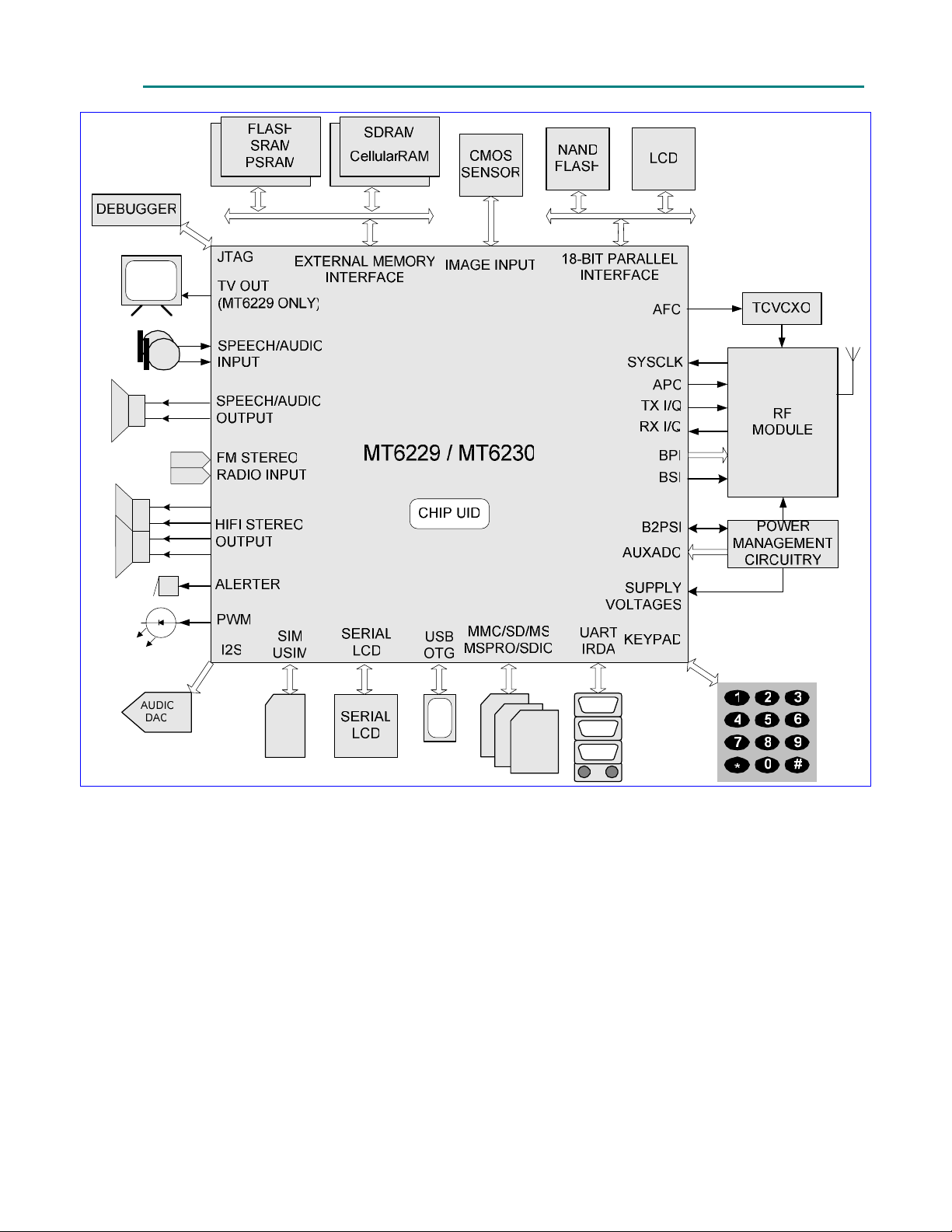
Typical application diagram is shown in Figure 1.
Platform
M
ARM7EJ-STM RISC processor at up to 104Mhz, thus
providing fast data processing capabilities. In addition to
the high clock frequency, separate CODE and DATA
caches are also added to further improve the overall system
efficiency.
For large amount of data transfer, high performance DMA
(Direct Memory Access) with hardware flow control is
implemented, which greatly enhances the data movement
speed while reducing MCU processing load.
Targeted as a media-rich platform for mobile applications,
MT6229 and MT6230 also provide hardware security
digital rights management for copyright protection. For
further safeguarding, and to protect manufacturer’s
development investment, hardware flash content protection
is also provided to prevent unauthorized porting of
software load.
Memory
T
maximum bandwidth for data intensive applications such
as multimedia features, MT6229 and MT6230 support up
to 4 external state-of-the-art devices through its 8/16-bit
host interface. High performance devices such as Mobile
RAM, and Cellular RAM are supported for maximum
bandwidth. Traditional devices such as burst/page mode
T6229 and MT6230 are capable of running the
o provide the greatest capacity for expansion and
Multi-media
he MT6229 multi-media subsystem provides connection
T
to CMOS image sensor and supports resolution up to 3M
pixels, while MT6230 supports up to 1.3M pixels. With
their advanced image signal and data processing
technology, both MT6229 and MT6230 allow efficient
processing of image and video data. MT6229 and MT6230
also have built-in JPEG CODEC and MPEG-4/H.263
CO
DEC, thus enabling real-time recording and playback
of high-quality images and video. Hardware
MPEG4/H.263 accelerator supports playback in VGA
mode at 15fps, and encoding in CIF at 15fps. Videophone
functionality is also provided. Moreover, high quality
de-blocking filter is provided to remove blocking artifacts
in video playback. GIF decoder and PNG decoder are
implemented as well for fast image decoding. MT6229 and
MT6230 also support TV-OUT capability, thus allowing
the mobile handset to connect to TV screen via NTSC/PAL
connections.
In addition to advanced image and video features, MT6229
and MT6230 also utilize high resolution audio DAC,
digital audio, and audio synthesis technology to provide
superior audio features for all future multi-media needs.
Connectivity, and Storage
n order to take advantage of its incredible multimedia
I
strengths, MT6229 and MT6230 incorporate myriads of
advanced connectivity and storage options for data storage
and communication. MT6229 and MT6230 support UART,
5
/667 MediaTek Inc. Confidential

M
T6229 / MT6230 GSM/GPRS/EDGE Baseband Processor Data Sheet Revision 2.01
Fast IrDA, USB 1.1 Full Speed OTG, SDIO, Bluetooth and
W
IFI Interface, and MMC/SD/MS/MS Pro storage
systems. All these interfaces provide MT6229 / MT6230
users with the highest degree of flexibility in implementing
solutions suitable for the targeted application.
To achieve a complete user interface, MT6229 / MT6230
also bring together all the necessary peripheral blocks for a
multi-media 2.75G phone. The peripheral blocks includes
the Keypad Scanner with the capability to detect multiple
key presses, SIM Controller, Alerter, Real Time Clock,
PWM, Serial LCD Controller, and General Purpose
Programmable I/Os.
Furthermore, to provide more configuration and bandwidth
for multi-media products, an additional 18-bit parallel
interface is incorporated. This interface enables connection
to LCD panels as well as connection to NAND flash
devices for additional multi-media data storage.
Audio
sing a highly integrated mixed-signal Audio Front-End,
U
architecture of both MT6229 and MT6230 allow for easy
audio interfacing with direct connection to the audio
transducers. The audio interface integrates D/A and A/D
Converters for Voice band, as well as high resolution
Stereo D/A Converters for Audio band. In addition,
MT6229 / MT6230 also provide Stereo Input and Analog
Mux.
expensive TCVCXO. MT6229 / MT6230 achieve great
MODEM performance by utilizing 14-bit high resolution
A/D Converter in the RF downlink path. Furthermore, to
reduce the need for extra external current-driving
component, the driving strength of some BPI outputs is
designed to be configurable.
Debug Function
T
he JTAG interface enables in-circuit debugging of
software program with the ARM7EJ-S core. With this
standardized debugging interface, MT6229 and MT6230
provide developers with a wide set of options in choosing
ARM development kits from different third party vendors.
Power Management
T6229 and MT6230 offer various low-power features to
M
help reduce system power consumption. These features
include Pause Mode of 32KHz clocking at Standby State,
Power Down Mode for individual peripherals, and
Processor Sleep Mode. In addition, MT6229 and MT6230
are also fabricated in advanced low leakage CMOS process,
hence providing an overall ultra low leakage solution.
Package
T
he MT6229 and MT6230 devices are offered in a
13mm×13mm, 314-ball, 0.65 mm pitch, TFBGA package.
MT6229 and MT6230 support AMR codec to adaptively
optimize speech and audio quality. Moreover, HE-AAC
codec is implemented to deliver CD-quality audio at low
bit rates.
On the whole, MT6229 and MT6230’s audio features
provide a rich solution for multi-media applications.
Radio
oth MT6229 / MT6230 integrate a mixed-signal
B
Baseband front-end in order to provide a well-organized
radio interface with flexibility for efficient customization.
It contains gain and offset calibration mechanisms, and
filters with programmable coefficients for comprehensive
compatibility control on RF modules. This approach also
allows the usage of a high resolution D/A Converter for
controlling VCXO or crystal, thus reducing the need for
6
/667 MediaTek Inc. Confidential
M
T6229 / MT6230 GSM/GPRS/EDGE Baseband Processor Data Sheet Revision 2.01
Figure
7
1 Typical application of MT6229 / MT6230.
/667 MediaTek Inc. Confidential

M
T6229 / MT6230 GSM/GPRS/EDGE Baseband Processor Data Sheet Revision 2.01
1.1 Platform Features
General
Integrated voice-band, audio-band and base-band
analog front ends
TFBGA 13mm×13mm, 313-ball, 0.65 mm pitch
package
MCU Subsystem
ARM7EJ-S 32-bit RISC processor
High performance multi-layer AMBA bus
Java hardware acceleration for fast Java-based
ga
mes and applets
Operating frequency: 26/52/104 MHz
Dedicated DMA bus
14 DMA channels
1M bits on-chip SRAM
1M bits MCU dedicated Tightly Coupled memory
256K bits CODE cache
Industry standard Parallel LCD Interface
Supports multi-media companion chips with 8/16
ts data width
bi
Flexible I/O voltage of 1.8V ~ 2.8V for memory
interface
Configurable driving strength for memory
interface
User Interfaces
6-row × 7-column keypad controller with
hardware scanner
Supports multiple key presses for gaming
SIM/USIM Controller with hardware T=0/T=1
protocol control
Real Time Clock (RTC) operating with a separate
po
wer supply
General Purpose I/Os (GPIOs)
2 Sets of Pulse Width Modulation (PWM) Output
64K bits DATA cache
On-chip boot ROM for Factory Flash
Pr
ogramming
Watchdog timer for system crash recovery
3 sets of General Purpose Timer
Circuit Switch Data coprocessor
Division coprocessor
PPP Framer coprocessor
External Memory Interface
Supports up to 4 external devices
Supports 8-bit or 16-bit memory components with
ma
ximum size of up to 64M Bytes each
Supports Mobile RAM, and Cellular RAM
Supports Flash and SRAM/PSRAM with Page
Mode or Burst Mode
Alerter Output with Enhanced PWM or PDM
8 external interrupt lines
Security
Cipher: supports AES, DES/3DES
Hash: supports MD5, SHA-1
Supports security key and 27 bit chip unique ID
Connectivity
3 UARTs with hardware flow control and speed up
to 921600 bps
IrDA modulator/demodulator with hardware
fr
amer. Supports SIR/MIR/FIR operating speeds.
Full-speed USB 1.1 OTG capability. Supports
device mode, limited host mode, and dual-role
OTG mode.
8
/667 MediaTek Inc. Confidential

M
M
ulti Media Card/Secure Digital Memory
T6229 / MT6230 GSM/GPRS/EDGE Baseband Processor Data Sheet Revision 2.01
Card/Memory Stick/Memory Stick Pro host
controller with flexible I/O voltage power
Supports SDIO interface for SDIO peripherals as
we
ll as WIFI connectivity
DAI/PCM and I2S interface for Audio application
Power Management
Power Down Mode for analog and digital circuits
Processor Sleep Mode
Pause Mode of 32KHz clocking at Standby State
7-channel Auxiliary 10-bit A/D Converter for
ch
arger and battery monitoring and photo sensing
Test and Debug
Built-in digital and analog loop back modes for
both Audio and Baseband Front-End
DAI port complying with GSM Rec.11.10
JTAG port for debugging embedded MCU
9
/667 MediaTek Inc. Confidential

M
T6229 / MT6230 GSM/GPRS/EDGE Baseband Processor Data Sheet Revision 2.01
1.2 MODEM Features
Radio Interface and Baseband Front End
GMSK/8PSK modulator with analog I and Q
channel outputs
10-bit D/A Converter for uplink baseband I and Q
signals
14-bit high resolution A/D Converter for downlink
baseband I and Q signals
Calibration mechanism of offset and gain
mi
smatch for baseband A/D Converter and D/A
Converter
10-bit D/A Converter for Automatic Power
Control
13-bit high resolution D/A Converter for
Automatic Frequency Control
Programmable Radio RX filter with adaptive
ba
ndwidth control
Dedicated Rx filter for FB acquisition
2 Channels Baseband Serial Interface (BSI) with
3-wire control
Bi-directional BSI interface. RF chip register read
access with 3-wire or 4-wire interface.
10-Pin Baseband Parallel Interface (BPI) with
pr
ogrammable driving strength
GSM/GPRS quad vocoders for adaptive multirate
MR), enhanced full rate (EFR), full rate (FR)
(A
and half rate (HR)
GSM channel coding, equalization and A5/1, A5/2
and A5/3 ciphering
GPRS/EGPRS GEA1, GEA2 and GEA3 ciphering
Programmable GSM/GPRS/EGPRS Modem
Packet Switched Data with CS1-CS4,
MC
S1-MCS9 coding schemes with full set IR
(Incremental Redundancy) support
GSM Circuit Switch Data
GPRS/EGPRS Class 12
Voice Interface and Voice Front End
Two microphone inputs sharing one low noise
am
plifier with programmable gain and automatic
gain control (AGC) mechanism
Voice power amplifier with programmable gain
2nd order Sigma-Delta A/D Converter for voice
uplink path
D/A Converter for voice downlink path
Supports half-duplex hands-free operation
Compliant with GSM 03.50
Multi-band support
Voice and Modem CODEC
Dial tone generation
Voice Memo
Noise Reduction
Echo Suppression
Advanced Sidetone Oscillation Reduction
Digital sidetone generator with programmable
ga
in
Two programmable acoustic compensation filters
1
0/667 MediaTek Inc. Confidential

M
T6229 / MT6230 GSM/GPRS/EDGE Baseband Processor Data Sheet Revision 2.01
1.3 Multi-Media Features
LCD/NAND Flash Interface
Dedicated Parallel Interface supports 3 external
devices with 8/16 bit NAND flash interface,
8/9/16/18 bit Parallel Interface, and Serial
interface for LCM
Built-in NAND Flash Controller with 1-bit ECC
for mass storages
Two chip selects available for high-density NAND
fl
ash device
LCD Controller
Supports simultaneous connection to up to 3
parallel LCD and 2 serial LCD modules
Supports LCM format: RGB332, RGB444,
RGB565, RGB666, RGB888
Supports LCD module with maximum resolution
up
to 800x600 at 24bpp
Per pixel alpha channel
True color engine
Supports hardware display rotation
Capable of combining display memories with up to
6 blending layers
Three Gamma correction tables
Image Signal Processor
8/10 bit Bayer format image input
YUV422/YCbCr422/RGB565 image input
Capable of processing image of size up to
MT6229: 3M pixels
MT6230: 1.3M pixels
Color Correction Matrix
Gamma Correction
Automatic Exposure Control
Automatic White Balance Control
Automatic Focus Control
Edge Enhancement
Color Suppression
Cross-talk compensation
Shading compensation
Defect Pixel compensation
Graphic Compression
GIF Decoder
PNG Decoder
JPEG Decoder
ISO/IEC 10918-1 JPEG Baseline and Progressive
modes
Supports all possible YUV formats, including
gr
ayscale format
Supports all DC/AC Huffman table parsing
Supports all quantization table parsing
Supports restart interval
Supports SOS, DHT, DQT and DRI marker
parsing
IEEE Std 1180-1990 IDCT Standard Compliant
Supports progressive image processing to
mi
nimize storage space requirement
Supports reload-able DMA for VLD stream
JPEG Encoder
ISO/IEC 10918-1 JPEG baseline mode
ISO/IEC 10918-2 Compliance
Supports YUV422 and YUV420 and grayscale
fo
rmats
Supports JFIF
Standard DC and AC Huffman tables
Provides 14 levels of encode quality
1
1/667 MediaTek Inc. Confidential

M
S
upports continuous shooting
T6229 / MT6230 GSM/GPRS/EDGE Baseband Processor Data Sheet Revision 2.01
Encoder resync marker and HEC
Image Data Processing
Support Digital Zoom
Support RGB888/565, YUV444 image processing
High throughput hardware scaler. Capable of
ta
iloring image to arbitrary size
Horizontal scaling in averaging method
Vertical scaling in bilinear method
Simultaneous scaling for MPEG-4 encode and
LC
D display
YUV and RGB color space conversion
Pixel format transform
Boundary padding
Pixel processing: hue/saturation/intensity/color
adjustment, Gamma correction and
grayscale/invert/sepia-tone effects
Programmable Spatial Filtering: Linear filter,
No
n-linear filter and Multi-pass artistic effects
Hardware accelerated image editing
Photo frame capability
RGB thumbnail data output
Supported visual tools for decoder: I-VOP, P-VOP,
C
/DC prediction, 4-MV, Unrestricted MV, Error
A
Resilience, Short Header
Error Resilience for decoder: Slice
Re
synchronization, Data Partitioning, Reversible
VLC
Supported visual tools for encoder: I-VOP, P-VOP,
Half-pel, DC prediction, Unrestricted MV,
Reversible VLC, Short Header
Supports encoding motion vector of range up
to
–64/+63.5 pixels
HE-AAC decode support
AAC/AMR/HE-AAC audio decode support
AMR audio encode support
TV-OUT
Supports NTSC/PAL formats (interlaced mode)
10 bit video DAC with 2x oversampling
Support one composite video output
2D Accelerator
Supports 32-bpp ARGB8888 and 24bpp RGB888
and 16-bpp RGB565 and 8-bpp index color modes
MPEG-4/H.263 CODEC
Hardware Video CODEC
ISO/IEC 14496-2 simple profile:
de
code @ level 0/1/2/3
encode @ level 0
ITU-T H.263 profile 0 @ level 10
Max decode speed is VGA @ 15fps
Max encode speed is CIF @ 15fps
Support VGA mode encoding
Horizontal and Vertical De-blocking filter in video
pl
ayback
Supports SVG Tiny acceleration
Rectangle gradient fill
BitBlt: multi-BitBlt with 7 rotation, 16 binary ROP
Alpha blending with 7 rotation
Line drawing: normal line, dotted line,
an
ti-aliasing
Circle drawing
Bezier curve drawing
Triangle flat fill
Font caching: normal font, Italic font
Command queue with max depth of 2047
2/667
1
MediaTek Inc. Confidential

M
T6229 / MT6230 GSM/GPRS/EDGE Baseband Processor Data Sheet Revision 2.01
A
udio CODEC
Support HE-AAC decode
Wavetable synthesis with up to 64 tones
Advanced wavetable synthesizer capable of
ge
nerating simulated stereo
Wavetable including GM full set of 128
instruments and 47 sets of percussions
PCM Playback and Record
Digital Audio Playback
Audio Interface and Audio Front End
Supports I2S interface
High resolution D/A Converters for Stereo Audio
playback
Stereo analog input for stereo audio source
Analog multiplexer for Stereo Audio
FM Radio Recording
Stereo to Mono Conversion
3/667
1
MediaTek Inc. Confidential

M
T6229 / MT6230 GSM/GPRS/EDGE Baseband Processor Data Sheet Revision 2.01
1.4 General Description
F
igure 2 details the block diagram of MT6229 and MT6230. Based on a dual-processor architecture, MT6229 / MT6230
i
ntegrate both an ARM7EJ-S core and 2 digital signal processor cores. ARM7EJ-S is the main processor that is responsible
for running high-level 2G to 2.75G protocol software as well as multi-media applications. Digital signal processors handle
the MODEM algorithms as well as advanced audio functions. Except for some mixed-signal circuitries, the other building
blocks in MT6229 and MT6230 are connected to either the microcontroller or one of the digital signal processor.
Specifically, both MT6229 and MT6230 consist of the following subsystems:
Microcontroller Unit (MCU) Subsystem - includes an ARM7EJ-S RISC processor and its accompanying memory
management and interrupt handling logics.
Digital Signal Processor (DSP) Subsystem - includes 2
DSP cores and their accompanying memory, memory
controller, and interrupt controller.
MCU/DSP Interface - where the MCU and the DSPs exchange hardware and software information.
Microcontroller Peripherals - includes all user interface modules and RF control interface modules.
Microcontroller Coprocessors - runs computing-intensive processes in place of Microcontroller.
DSP Peripherals - hardware accelerators for GSM/GPRS/EGDE channel codec.
Multi-media Subsystem - integrates several advanced a
Voice Front End - the data path for converting analog speech from and to digital speech.
Audio Front End - the data path for converting stereo audio from stereo audio source
Video Front End - the data path for converting video signal to NTSL/PAL format.
Baseband Front End - the data path for converting digital signal from and to analog signal of RF modules.
Timing Generator - generates the control signals related to the TDMA frame timing.
Power, Reset and Clock subsystem - manages the power,
ccelerators to support multi-media applications.
reset, and clock distribution inside MT6229 and
MT6230.
Details of the individual subsystems and blocks are described in following Chapters. By default, except CMOS sensor
interface, all features are identical for MT6229 and MT6230, and those descriptions related to MT6229 can also be applied
to MT6230.
4/667
1
MediaTek Inc. Confidential
M
T6229 / MT6230 GSM/GPRS/EDGE Baseband Processor Data Sheet Revision 2.01
MIC-0
MIC-1
VOICE
UDIO-L
A
AUDIO-R
STEREO-L
STEREO-R
RX-I
X-Q
R
TX-I
TX-Q
AUXADC
A
APC
ADC
DAC
AUDIO
P
DAC
+
DAC
+
ADC
ADC
BASEBAND
ATH
ADC
TV-OUT
ON
C
P
AUX
DC
A
DAC
DAC
FC
DAC AFC
DACTVOUT
DAC APC
ATH
BRIDGE
INTERRUPT
ONTROL
C
2D
NGINE
E
IMAGE
MA
D
PATCH
U
NITS
MCU/DSP
I
NTERFACE
CACHE
ARM7EJ-S
GRAPHIC MEMORY
IMAGE
OST
P
PROC’
MEMORY
DSP1
ONTROLLER
C
BOOT
R
OM
SECURITY
NGINE
E
TCM
GIF/PNG
ECODE
D
DSP2
JPEG
C
TRAP
U
NITS
C
ONTROL
ODEC
DMA
ON-CHIP
RAM
S
INTERRUPT
ONTROL
C
MPEG-4
IDEO
V
CODEC
USB OTG
COPROC
E
SSOR
COPROC
SSOR
E
COPROC
E
SSOR
CACHE
EXTERNAL
EMORY
M
INTERFACE
NAND
F
COPROC
E
COPROC
E
COPROC
E
LCD
ON
C
LASH
CON
SSOR
SSOR
SSOR
USB OTG
SDRAM
CellularRAM
FLASH
SRAM
PSRAM
NAND
CD
L
SERIAL RF
CONTROL
PARALLEL
RF CONTROL
SYSTEM
LOCK
C
13/26MHZ
BSI
BPI
CLOCK
EN
G
32K
SC
O
32KHZ
CRYSTAL
TDMA
IMER
T
RTC
WAKE UP
GPT
WDT
RESET
Figure 2 M
IMAGE RESIZER
SIM GPIO
PWM
USER
INTERFACE
KEYPAD
ALERTER
B2PSI IRDA
SERIAL
CD
L
SERIAL PORT
T6229 / MT6230 block diagram.
MMC
D/MS
S
MS PRO
C
ONNECTIVITY
UART
IMAGE
IGNAL
S
PROC’
SCCB
M
MT6230
T6229
CMOS
ENSOR
S
5/667
1
MediaTek Inc. Confidential

M
T6229 / MT6230 GSM/GPRS/EDGE Baseband Processor Data Sheet Revision 2.01
2 Product Descriptions
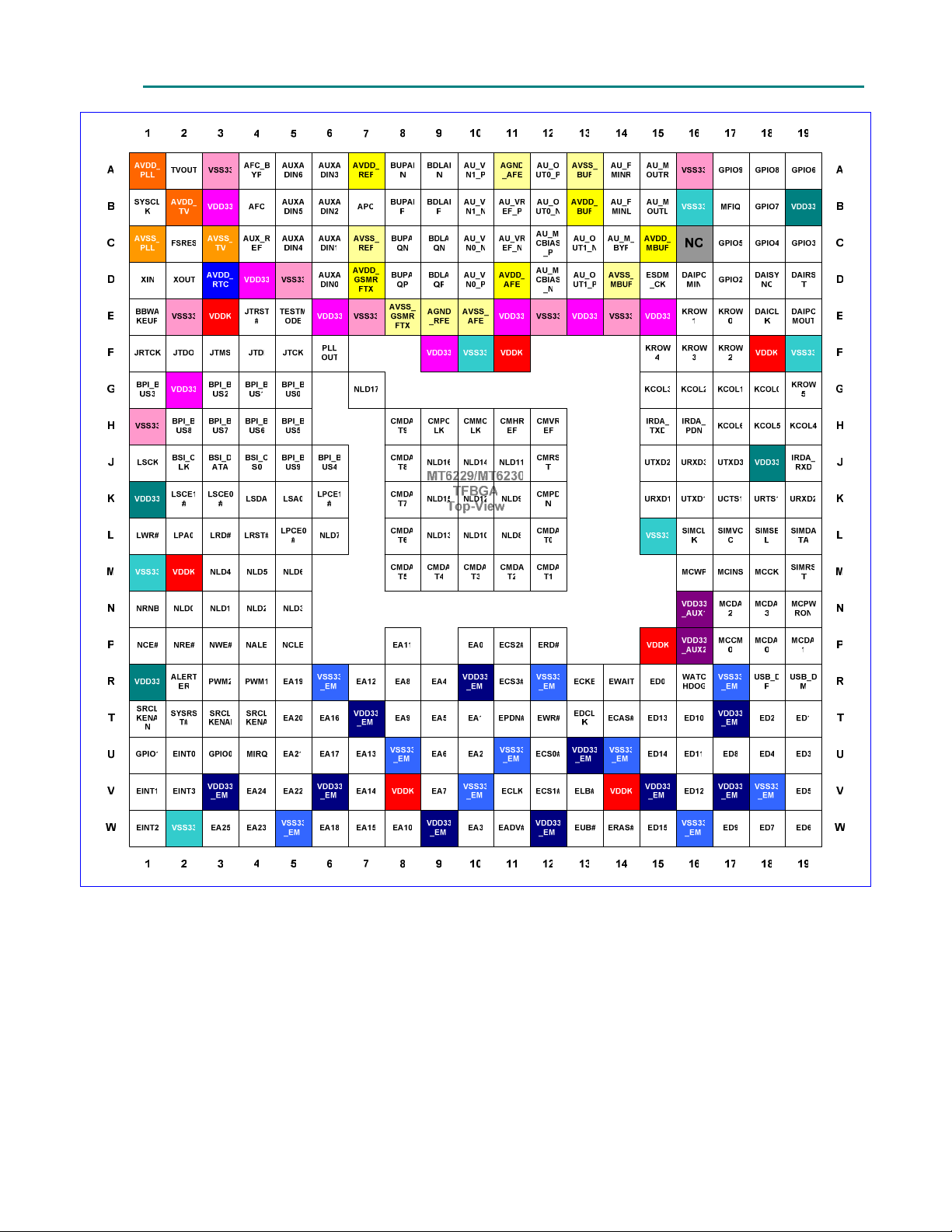
2.1
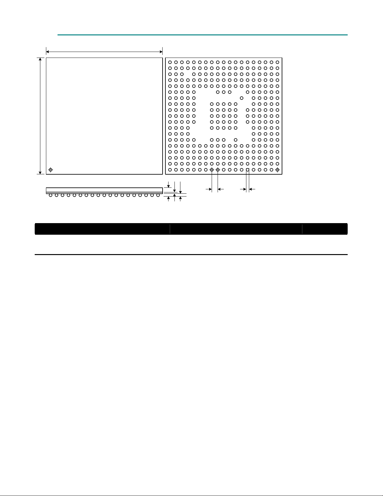
One type of package for this product, TFBGA 13mm*13mm
MT6229 / MT6230 are pin-to-pin compatible to MT6228 except one VDDK ball @P15.
Pin-outs and the top view are illustrated in Figure 3 for this package. Outline and dimension of package is illustrated in
Figure 4, while the definition of package is shown in Table 1.
Pin Outs
, 314-ball, 0.65 mm pitch Package, is offered. Note that
6/667
1
MediaTek Inc. Confidential
M
T6229 / MT6230 GSM/GPRS/EDGE Baseband Processor Data Sheet Revision 2.01
Figure 3 T
op View of MT6229 (MT6230) TFBGA 13mm*13mm, 314-ball, 0.65 mm pitch Package
7/667
1
MediaTek Inc. Confidential
M
T6229 / MT6230 GSM/GPRS/EDGE Baseband Processor Data Sheet Revision 2.01
D
E
MT6229 / MT6230
T
op View
(Pins Down)
A C A1
1516171819
MT6229 / MT6230
e b
B
View
15 4 3 2610 9 8 711121314
A
B
C
D
E
F
G
H
J
K
L
M
N
P
R
Y
U
V
W
ottem
Figure 4 Outlines and Dimension of TFBGA 13mm*13mm, 314-ball, 0.65 mm pitch Package
Body Size Ball Count Ball Pitch Ball Dia. Package Thk. Stand Off Substrate Thk.
D E N E
13 13 314 0
B A (Max.) A1 C
.65 0.3 1.2 0.3 0.36
Table 1
Definition of TFBGA 13mm*13mm, 314-ball, 0.65 mm pitch Package (Unit: mm)
8/667
1
MediaTek Inc. Confidential
M
T6229 / MT6230 GSM/GPRS/EDGE Baseband Processor Data Sheet Revision 2.01
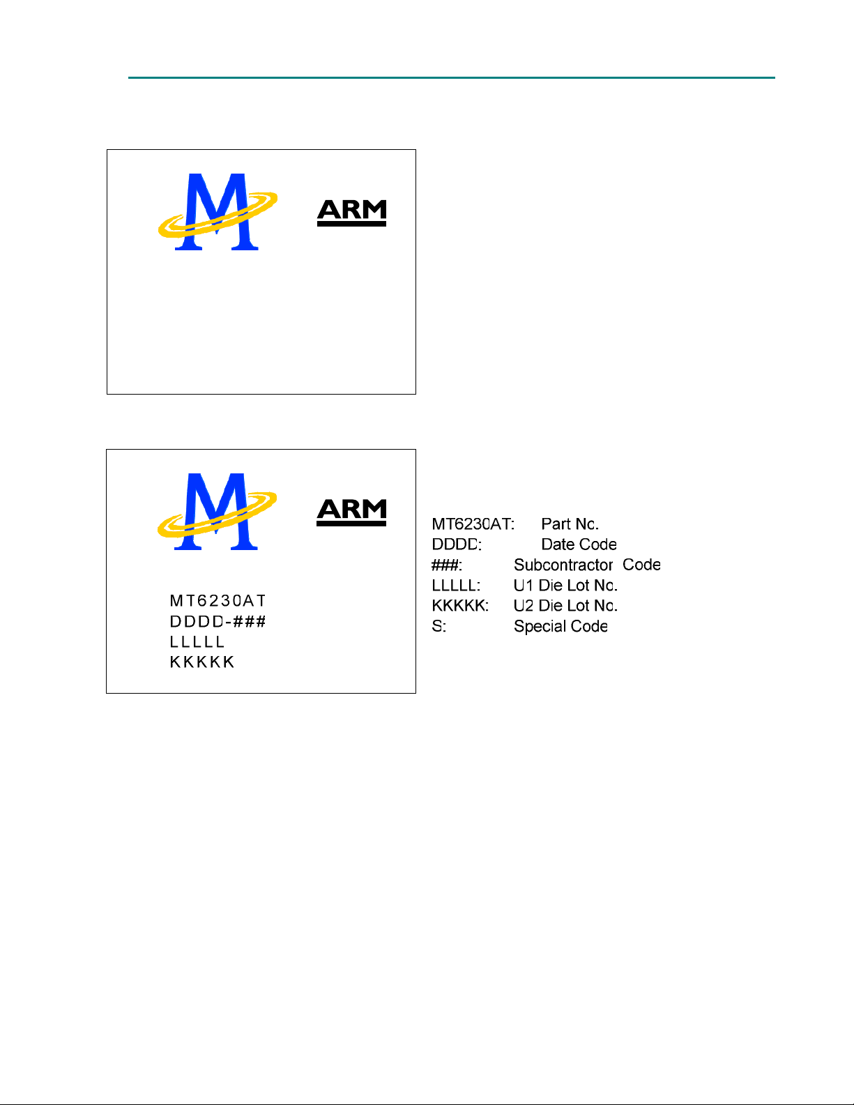
2.2 Top Marking Definition
M T 6 2 2 9 A T
D D D D - # # #
L L L L L
K K K K K
S
MT6229AT: Part No.
DDDD: Date Code
###: Subcontractor Code
LLLLL: U1 Die Lot No.
KKKKK: U2 Die Lot No.
S: Special Code
S
9/667
1
MediaTek Inc. Confidential

M
T6229 / MT6230 GSM/GPRS/EDGE Baseband Processor Data Sheet Revision 2.01
DC Characteristics
2
.2.1 Absolute Maximum Ratings
Prolonged exposure to absolute maximum ratings may re
ratings is not implied.
Item Symbol Min Max Unit
IO power supply V
I/O input voltage V
Operating temperature T
Storage temperature T
DD33 -0.3 VDD33+0.3 V
DD33I -0.3 VDD33+0.3 V
opr -20 80 Celsius
stg -55 125 Celsius
duce device reliability. Functional operation at these maximum
0/667
2
MediaTek Inc. Confidential

M
T6229 / MT6230 GSM/GPRS/EDGE Baseband Processor Data Sheet Revision 2.01
2.3 Pin Description
elow pin description is identical for both MT6229 and MT6230.
B
Ball
13X13
E4
F5
F4
F3
F2
F1
G5
G4
G3
G1
J6
H5
H4 BPI_BUS6 IO RF hard-wire control bus 6
H3 BPI_BUS7 IO RF hard-wire control bus 7
H2 BPI_BUS8 IO RF hard-wire control bus 4
J5 BPI_BUS9 IO RF hard-wire control bus 5
J4
J3
J2
R4 PWM1 I
R3 PWM2 I
R2 ALERTER IO Pulse width modulated signal for buzzer
J1 LSCK I
K5 LSA0 I
K4 LSDA I
K3 LSCE0# I
K2 LSCE1# I
K6 LPCE1# I
L5
L4
L3
L2
L1
G7 NLD17 I
J9 NLD16 I
K9
J10
L9
K10
J11
L10
K11
N
ame Dir Description
RST#
JT
JT
CK
DI
JT
JT
MS
DO
JT
TCK
JR
PI_BUS0
B
PI_BUS1
B
PI_BUS2
B
PI_BUS3
B
PI_BUS4
B
PI_BUS5
B
SI_CS0
B
SI_DATA
B
SI_CLK
B
PCE0#
L
RST#
L
RD#
L
PA0
L
WR#
L
LD15
N
LD14
N
DL13
N
LD12
N
LD11
N
LD10
N
LD9
N
JTAG Port
I JTAG test port reset input PD Input
I JTAG test port clock input PU Input
I JTAG test port data input PU Input
I JTAG test port mode switch PU Input
O JTAG test port data output 0
O JTAG test port returned clock output 0
RF Parallel Control Unit
O RF hard-wire control bus 0 0
O RF hard-wire control bus 1 0
O RF hard-wire control bus 2 0
O RF hard-wire control bus 3 0
O RF hard-wire control bus 4
O RF hard-wire control bus 5
RF Serial Control Unit
O RF 3-wire interface chip select 0
IO RF 3-wire interface data output
O RF 3-wire interface clock output
PWM Interface
O Pulse width modulated signal 1
O Pulse width modulated signal 2
Serial LCD/PM IC Interface
O Serial display interface data output
O Serial display interface address output
O Serial display interface clock output
O Serial display interface chip select 0 output
O Serial display interface chip select 1 output
Parallel LCD/NAND-Flash Interface
O Parallel display interface chip select 1 output
O Parallel display interface chip select 0 output
O Parallel display interface Reset Signal
O Parallel display interface Read Strobe
O Parallel display interface address output
O Parallel display interface Write Strobe
O Parallel LCD/NAND-Flash Data 17
O Parallel LCD/NAND-Flash Data 16
IO Parallel LCD/NAND-Flash Data 15
IO Parallel LCD/NAND-Flash Data 14
IO Parallel LCD/NAND-Flash Data 13
IO Parallel LCD/NAND-Flash Data 12
IO Parallel LCD/NAND-Flash Data 11
IO Parallel LCD/NAND-Flash Data 10
IO Parallel LCD/NAND-Flash Data 9
PU/P
Mode0 Mode1 Mode2 Mode3
PIO16
G
PIO17
G
PIO18
G
PIO19
G
GPIO32
GPIO33
PIO34
G
GPIO20
GPIO21
GPIO22
GPIO23
GPIO24
GPIO25
GPIO11
GPIO10
NLD15
NLD14
NLD13
NLD12
NLD11
NLD10
NLD9
0
0
BPI_BUS6
BPI_BUS7 13MHz 26MHz PD Input
BPI_BUS8 6.5MHz 32KHz PD Input
BPI_BUS9 BSI_CS1 BFEPRBO PD Input
PWM1 TBTXFS D2_TID2 PD Input
PWM2 TBRXEN D2_TID3 PD Input
ALERTER TBRXFS D2_TID4 PD Input
LSCK TDMA_CK TBTXEN PU Input
LSA0 TDMA_D1 TDTIRQ PU Input
LSDA TDMA_D0 TCTIRQ2 PU Input
LSCE0# TDMA_FS TCTIRQ1 PU Input
LSCE1# LPCE2# TEVTVAL PU Input
LPCE1# NCE1# D2_TID0 PU Input
1
1
1
1
1
NLD17 MCDA4 D2_TID1 PD Input
NLD16 MCDA5 D2ID PD Input
GPIO61 D2IMS PD Input
GPIO60 D2ICK PD Input
GPIO59 SWDBGPKT
GPIO58 SWDBGWR
GPIO57 SWDBGRD PD Input
GPIO56 SWDBGROE
GPIO55 SWDBGA0 PD Input
D
PD Input
0
0
0
PD Input
PD Input
PD Input
Reset
1/667
2
MediaTek Inc. Confidential

M
T6229 / MT6230 GSM/GPRS/EDGE Baseband Processor Data Sheet Revision 2.01
L11
L6
M5
M4
M3
N5
N4
N3
N2
N1
P5
P4
P3
P2
P1
M19
L16
L17
L18 SIMSEL O
L19
U3
U1
D17
C19
C18
C17
A19
B18
A18
A17
T2
R16
T1
T4
T3 SRCLKENAI IO External TCXO enable input
E5
D15
H17
H18
H19
G15
G16
G17
G18
G19
F15
F16
F17
E16
E17
N
LD8
N
LD7
N
LD6
LD5
N
N
LD4
LD3
N
N
LD2
LD1
N
N
LD0
RNB
N
N
CLE
ALE
N
WE#
N
RE#
N
CE#
N
IMRST
S
IMCLK
S
IMVCC
S
IMDATA
S
PIO0
G
PIO1
G
PIO2
G
PIO3
G
PIO4
G
PIO5
G
PIO6
G
PIO7
G
PIO8
G
PIO9
G
YSRST#
S
ATCHDOG#
W
RCLKENAN
S
RCLKENA
S
ESTMODE
T
SDM_CK
E
COL6
K
COL5
K
COL4
K
COL3
K
COL2
K
COL1
K
COL0
K
ROW5
K
ROW4
K
ROW3
K
ROW2
K
ROW1
K
ROW0
K
IO Parallel LCD/NAND-Flash Data 8
IO Parallel LCD/NAND-Flash Data 7
IO Parallel LCD/NAND-Flash Data 6
IO Parallel LCD/NAND-Flash Data 5
IO Parallel LCD/NAND-Flash Data 4
IO Parallel LCD/NAND-Flash Data 3
IO Parallel LCD/NAND-Flash Data 2
IO Parallel LCD/NAND-Flash Data 1
IO Parallel LCD/NAND-Flash Data 0
IO NAND-Flash Read/Busy Flag
IO NAND-Flash Command Latch Signal
IO NAND-Flash Address Latch Signal
IO NAND-Flash Write Strobe
IO NAND-Flash Read Strobe
IO NAND-Flash Chip select output
SIM Card Interface
O SIM card reset output 0
O SIM card clock output 0
O SIM card supply power control 0
SIM card supply power select
IO SIM card data input/output 0
Dedicated GPIO Interface
IO General purpose input/output 0
IO General purpose input/output 1
IO General purpose input/output 2
IO General purpose input/output 3
IO General purpose input/output 4
IO General purpose input/output 5
IO General purpose input/output 6
IO General purpose input/output 7
IO General purpose input/output 19
IO General purpose input/output 21
Miscellaneous
I System reset input active low Input
O Watchdog reset output 1
O External TCXO enable output active low GPO1
O External TCXO enable output active high GPO0
I TESTMODE enable input
O Internal Monitor Clock
Keypad Interface
I Keypad column 6 PU Input
I Keypad column 5 PU Input
I Keypad column 4 PU Input
I Keypad column 3 PU Input
I Keypad column 2 PU Input
I Keypad column 1 PU Input
I Keypad column 0 PU Input
O Keypad row 5
O Keypad row 4
O Keypad row 3
O Keypad row 2
O Keypad row 1 0
O Keypad row 0 0
NLD8
NRNB
NCLE
NALE
NWE#
NRE#
NCE#
GPIO48
GPIO0
GPIO1
GPIO2
GPIO3
GPIO4
GPIO5
GPIO6
GPIO7
GPIO8
(EINT7)
GPIO9
PIO35
G
(EINT5)
KROW5
KROW4
KROW3
KROW2
GPIO54 SWDBGA1 PD Input
PD Input
PD Input
PD Input
PD Input
PD Input
PD Input
PD Input
PD Input
GPIO26 USBSESSVLD
GPIO27
GPIO28 USBSESSEND
GPIO29 PU
GPIO30
GPIO31 PU
SIMSEL PD Input
CMFLASH D2_TID5 PD Input
BSI_RFIN PD Input
SCL PU Input
SDA PU Input
EDICK URXD2
EDIWS UTXD2 SWDBGD6
EDIDAT SWDBGD5
USBVBUSON
32KHz
26MHz 13MHz SWDBGE
SRCLKENA
N
SRCLKENA
SRCLKENAI PD Input
GPIO44 ARM CK TV CK 0
GPIO45 AHB CK DSP CK 0
GPIO46 FTV CK SLOW CK 0
GPIO47 FMCU CK FUSB CK 0
USBVBUSVLD
USBVBUSDSC
(EINT6)
USBVBUSCHG
0
1
PD Input
SWDBGD2 PU
SWDBGD1 PD
SWDBGD0 PD
SWDBGCK PU
SWDBGD7
SWDBGD4
SWDBGF
2/667
2
MediaTek Inc. Confidential

M
T6229 / MT6230 GSM/GPRS/EDGE Baseband Processor Data Sheet Revision 2.01
U2
V1
W1
V2
U4 MIRQ I
B17 MFIQ I
R15
T19
T18
U19
U18
V19
W19
W18
U17
W17
T16
U16
V16
T15
U15
W15
P12
T12
U12
V12
P11
R11
R14
T14
W14
R13
T13
V13
W13
T11
W11
V11
P10
T10
U10
W10
R9
T9
U9
V9
R8
T8
W8
P8
R7
U7
V7
W7
T6
E
INT0
E
INT1
INT2
E
INT3
E
E
D0
D1
E
D2
E
D3
E
D4
E
D5
E
D6
E
D7
E
D8
E
D9
E
D10
E
D11
E
D12
E
D13
E
D14
E
D15
E
RD#
E
WR#
E
CS0#
E
CS1#
E
CS2#
E
CS3#
E
WAIT
E
CAS#
E
RAS#
E
CKE
E
DCLK
E
LB#
E
UB#
E
PDN#
E
ADV#
E
CLK
E
A0
E
A1
E
A2
E
A3
E
A4
E
A5
E
A6
E
A7
E
A8
E
A9
E
A10
E
A11
E
A12
E
A13
E
A14
E
A15
E
A16
E
External Interrupt Interface
I External interrupt 0 PU Input
I External interrupt 1 PU Input
I External interrupt 2 PU Input
I External interrupt 3 PU Input
Interrupt to MCU
Interrupt to MCU
External Memory Interface
IO External memory data bus 0 Input
IO External memory data bus 1 Input
IO External memory data bus 2 Input
IO External memory data bus 3 Input
IO External memory data bus 4 Input
IO External memory data bus 5 Input
IO External memory data bus 6 Input
IO External memory data bus 7 Input
IO External memory data bus 8 Input
IO External memory data bus 9 Input
IO External memory data bus 10 Input
IO External memory data bus 11 Input
IO External memory data bus 12 Input
IO External memory data bus 13 Input
IO External memory data bus 14 Input
IO External memory data bus 15 Input
O External memory read strobe 1
O External memory write strobe 1
O External memory chip select 0 1
O External memory chip select 1 1
O External memory chip select 2 1
O External memory chip select 3 1
O Flash, PSRAM and CellularRAM data ready
O MobileRAM column address
O MobileRAM row address
O MobileRAM clock enable
O MobileRAM clock
O External memory lower byte strobe
O External memory upper byte strobe
O PSRAM power down control GPO2
O Flash, PSRAM and CellularRAM address valid 1
O Flash, PSRAM and CellularRAM clock 0
O External memory address bus 0 0
O External memory address bus 1 0
O External memory address bus 2 0
O External memory address bus 3 0
O External memory address bus 4 0
O External memory address bus 5 0
O External memory address bus 6 0
O External memory address bus 7 0
O External memory address bus 8 0
O External memory address bus 9 0
O External memory address bus 10 0
O External memory address bus 11 0
O External memory address bus 12 0
O External memory address bus 13 0
O External memory address bus 14 0
O External memory address bus 15 0
O External memory address bus 16 0
GPIO36
GPIO63
MIRQ 6.5MHz 32KHz PU Input
MFIQ USBID
PU Input
1
1
1
EPDN#
(EINT8)
1
1
26Mhz 13MHz 0
SWDBGD3 PU Input
3/667
2
MediaTek Inc. Confidential

M
T6229 / MT6230 GSM/GPRS/EDGE Baseband Processor Data Sheet Revision 2.01
U6
W6
R5
T5
U5
V5
W4
V4
W3
R18
R19
P17
P18
P19
N17
N18
M18
N19
M16
M17
K15
K16
K17
K18
K19 URXD2 I
J15 UTXD2 I
J16 URXD3 I
J17 UTXD3 I
J19 IRDA_RXD IO IrDA receive data
H15 IRDA_TXD IO IrDA transmit data
H16 IRDA_PDN IO IrDA Power Down Control
E18 DAICLK IO DAI clock output
E19 DAIPCMOUT IO DAI pcm data out
D16 DAIPCMIN IO DAI pcm data input
D19 DAIRST IO DAI reset signal input
D18 DAISYNC IO DAI frame synchronization signal output
J12 CMRST I
K12 CMPDN IO CMOS sensor power down control
H12
H11
H9
H10
H8
J8
K8
L8
M8
E
A17
E
A18
E
A19
A20
E
E
A21
A22
E
E
A23
A24
E
E
A25
U
SB_DP
SB_DM
U
M
CCM0
CDA0
M
CDA1
M
CDA2
M
CDA3
M
CCK
M
CPWRON
M
CWP
M
CINS
M
RXD1
U
TXD1
U
CTS1
U
RTS1
U
MVREF
C
MHREF
C
MPCLK
C
MMCLK
C
MDAT9
C
MDAT8
C
MDAT7
C
MDAT6
C
MDAT5
C
O External memory address bus 17 0
O External memory address bus 18 0
O External memory address bus 19 0
O External memory address bus 20
O External memory address bus 21
O External memory address bus 22 0
O External memory address bus 23 0
O External memory address bus 24
O External memory address bus 25
USB Interface
IO USB D+ Input/Output
IO USB D- Input/Output
Memory Card Interface
IO SD Command/MS Bus State Output PU/PD
IO SD Serial Data IO 0/MS Serial Data IO PU/PD
IO SD Serial Data IO 1 PU/PD
IO SD Serial Data IO 2 PU/PD
IO SD Serial Data IO 3 PU/PD
O SD Serial Clock/MS Serial Clock Output
O SD Power On Control Output
I SD Write Protect Input
I SD Card Detect Input
UART/IrDA Interface
I UART 1 receive data
O UART 1 transmit data
I UART 1 clear to send
O UART 1 request to send
O UART 2 receive data
O UART 2 transmit data
O UART 3 receive data
O UART 3 transmit data
Digital Audio Interface
CMOS Sensor Interface
O CMOS sensor reset signal output
I Sensor vertical reference signal input
I Sensor horizontal reference signal input
I CMOS sensor pixel clock input
O CMOS sensor master clock output
I CMOS sensor data input 9
I CMOS sensor data input 8
I CMOS sensor data input 7
I CMOS sensor data input 6
I CMOS sensor data input 5
GPIO37
GPIO38
GPIO39
GPIO40
PIO41
G
PIO42
G
PIO43
G
PIO49
G
PIO50
G
PIO51
G
PIO52
G
PIO53
G
GPIO12
PIO13
G
CMDAT9
CMDAT8
CMDAT7
CMDAT6
CMDAT5
0
0
PU
PU/PD Input
URXD2
(EINT6)
UTXD2 URTS3 PU Input
URXD3 D1ID PU Input
UTXD3 D2_TID6 PU Input
IRDA_RXD UCTS2 SWDBGD15
IRDA_TXD URTS2 SWDBG14 PU Input
IRDA_PDN SWDBG13 PU Input
DAICLK SWDBGD12
DAIPCMOUT
DAIPCMIN SWDBGD10
DAIRST SWDBG9 PU Input
DAISYNC SWDBG8 PU Input
CMRST D1_TID0 PD Input
CMPDN D1_TID1 PD Input
PD Input
PD Input
PD Input
0
GPIO74 PD Input
GPIO73 PD Input
GPIO72 PD Input
GPIO71 PD Input
GPIO70 PD Input
UCTS3 PU Input
S
WDBGD11
0
0
PU Input
1
PU Input
1
PU Input
PU Input
PD Input
PU Input
4/667
2
MediaTek Inc. Confidential

M
T6229 / MT6230 GSM/GPRS/EDGE Baseband Processor Data Sheet Revision 2.01
M9
M10
M11
M12 CMDAT1 IO CMOS sensor data input 1
L12 CMDAT0 IO CMOS sensor data input 0
B15
A15
C14
B14
A14
D13
C13
B12
A12
C12
D12
C11
B11
D10
C10
B10
A10
D9
C9
A9
B9
B8
A8
C8
D8
B7
D6
C6
B6
A6
C5
B5
A5
C4
B4
A4
B1
F6
D1
D2
E1
A2
C2
E3
M2
V8
V14
C
MDAT4
C
MDAT3
C
MDAT2
A
U_MOUL
U_MOUR
A
A
U_M_BYP
U_FMINL
A
A
U_FMINR
U_OUT1_P
A
A
U_OUT1_N
U_OUT0_N
A
A
U_OUT0_P
U_MICBIAS_P
A
U_MICBIAS_N
A
U_VREF_N
A
U_VREF_P
A
U_VIN0_P
A
U_VIN0_N
A
U_VIN1_N
A
U_VIN1_P
A
DLAQP
B
DLAQN
B
DLAIN
B
DLAIP
B
UPAIP
B
UPAIN
B
UPAQN
B
UPAQP
B
PC
A
UXADIN0
A
UXADIN1
A
UXADIN2
A
UXADIN3
A
UXADIN4
A
UXADIN5
A
UXADIN6
A
UX_REF
A
FC
A
FC_BYP
A
YSCLK
S
LLOUT
P
IN
X
OUT
X
BWAKEUP
B
VOUT
T
SRES
F
DDK
V
DDK
V
DDK
V
DDK
V
I CMOS sensor data input 4
I CMOS sensor data input 3
I CMOS sensor data input 2
Analog Interface
Audio analog output left channel
Audio analog output right channel
Audio DAC bypass pin
FM radio analog input left channel
FM radio analog input right channel
Earphone 1 amplifier output (+)
Earphone 1 amplifier output (-)
Earphone 0 amplifier output (-)
Earphone 0 amplifier output (+)
Microphone bias supply (+)
Microphone bias supply (-)
Audio reference voltage (-)
Audio reference voltage (+)
Microphone 0 amplifier input (+)
Microphone 0 amplifier input (-)
Microphone 1 amplifier input (-)
Microphone 1 amplifier input (+)
Quadrature input (Q+) baseband codec downlink
Quadrature input (Q-) baseband codec downlink
In-phase input (I+) baseband codec downlink
In-phase input (I-) baseband codec downlink
In-phase output (I+) baseband codec uplink
In-phase output (I-) baseband codec uplink
Quadrature output (Q+) baseband codec uplink
Quadrature output (Q-) baseband codec uplink
Automatic power control DAC output
Auxiliary ADC input 0
Auxiliary ADC input 1
Auxiliary ADC input 2
Auxiliary ADC input 3
Auxiliary ADC input 4
Auxiliary ADC input 5
Auxiliary ADC input 6
Auxiliary ADC reference voltage input
Automatic frequency control DAC output
Automatic frequency control DAC bypass
capacitance
VCXO Interface
13MHz or 26MHz system clock input
PLL reference voltage output
RTC Interface
32.768 KHz crystal input
32.768 KHz crystal output
O Baseband power on/off control 1
TV Interface
TV DAC Output
Supply Voltages
Supply voltage of internal logic
Supply voltage of internal logic
Supply voltage of internal logic
Supply voltage of internal logic
CMDAT4
CMDAT3
CMDAT2
PIO14
G
G
PIO15
GPIO69 PD Input
GPIO68 PD Input
GPIO62 PD Input
CMDAT1 D1IMS PD Input
CMDAT0 D1ICK PD Input
5/667
2
MediaTek Inc. Confidential

M
T6229 / MT6230 GSM/GPRS/EDGE Baseband Processor Data Sheet Revision 2.01
F18
F11
P15
V3
V6
T7
W9
R10
W12
U13
V15
T17
V17
W5
R6
U8
V10
U11
R12
U14
W16
R17
V18
P16
N16
G2
K1
R1
J18
B19
E15
E13
E11
F9
E6
D4
B3
W2
E2
H1
M1
L15
F19
V
DDK
V
DDK
V
DDK
DD33_EMI
V
V
DD33_EMI
DD33_EMI
V
DD33_EMI
V
V
DD33_EMI
DD33_EMI
V
V
DD33_EMI
DD33_EMI
V
V
DD33_EMI
DD33_EMI
V
V
SS33_EMI
SS33_EMI
V
SS33_EMI
V
SS33_EMI
V
SS33_EMI
V
SS33_EMI
V
SS33_EMI
V
SS33_EMI
V
SS33_EMI
V
SS33_EMI
V
DD33_AUX2
V
DD33_AUX1
V
DD33
V
DD33
V
DD33
V
DD33
V
DD33
V
DD33
V
DD33
V
DD33
V
DD33
V
DD33
V
DD33
V
DD33
V
SS33
V
SS33
V
SS33
V
SS33
V
SS33
V
SS33
V
Supply voltage of internal logic
Supply voltage of internal logic
Supply voltage of internal logic
Supply voltage of memory interface driver
Supply voltage of memory interface driver
Supply voltage of memory interface driver
Supply voltage of memory interface driver
Supply voltage of memory interface driver
Supply voltage of memory interface driver
Supply voltage of memory interface driver
Supply voltage of memory interface driver
Supply voltage of memory interface driver
Supply voltage of memory interface driver
Ground of memory interface driver
Ground of memory interface driver
Ground of memory interface driver
Ground of memory interface driver
Ground of memory interface driver
Ground of memory interface driver
Ground of memory interface driver
Ground of memory interface driver
Ground of memory interface driver
Ground of memory interface driver
Supply voltage of drivers for USB
Supply Voltage of MS/MMC/SD
Supply voltage of drivers except memory
interface, USB and MS/MMC/SD
Supply voltage of drivers except memory
interface, USB and MS/MMC/SD
Supply voltage of drivers except memory
interface, USB and MS/MMC/SD
Supply voltage of drivers except memory
interface, USB and MS/MMC/SD
Supply voltage of drivers except memory
interface, USB and MS/MMC/SD
Supply voltage of drivers except memory
interface, USB and MS/MMC/SD
Supply voltage of drivers except memory
interface, USB and MS/MMC/SD
Supply voltage of drivers except memory
interface, USB and MS/MMC/SD
Supply voltage of drivers except memory
interface, USB and MS/MMC/SD
Supply voltage of drivers except memory
interface, USB and MS/MMC/SD
Supply voltage of drivers except memory
interface, USB and MS/MMC/SD
Supply voltage of drivers except memory
interface, USB and MS/MMC/SD
Ground of drivers except memory interface, USB
and MS/MMC/SD
Ground of drivers except memory interface, USB
and MS/MMC/SD
Ground of drivers except memory interface, USB
and MS/MMC/SD
Ground of drivers except memory interface, USB
and MS/MMC/SD
Ground of drivers except memory interface, USB
and MS/MMC/SD
Ground of drivers except memory interface, USB
and MS/MMC/SD
6/667
2
MediaTek Inc. Confidential

M
T6229 / MT6230 GSM/GPRS/EDGE Baseband Processor Data Sheet Revision 2.01
B16
A16
E14
E12
F10
E7
D5
A3
A1
C1
B2
C3
D3
C15
D14
B13
A13
D11
A11
E10
E9
E8
D7
V
SS33
V
SS33
SS33
V
SS33
V
V
SS33
V
SS33
SS33
V
SS33
V
VDD_PLL
A
VSS_PLL
A
VDD_TV
A
VSS_TV
A
VDD_RTC
A
VDD_MBUF
A
VSS_MBUF
A
VDD_BUF
A
VSS_BUF
A
VDD_AFE
A
GND_AFE
A
VSS_AFE
A
GND_RFE
A
VSS_GSMRFTX
A
VDD_GSMRFTX
A
Ground of drivers except memory interface, USB
and MS/MMC/SD
Ground of drivers except memory interface, USB
and MS/MMC/SD
Ground of drivers except memory interface, USB
and MS/MMC/SD
Ground of drivers except memory interface, USB
and MS/MMC/SD
Ground of drivers except memory interface, USB
and MS/MMC/SD
Ground of drivers except memory interface, USB
and MS/MMC/SD
Ground of drivers except memory interface, USB
and MS/MMC/SD
Ground of drivers except memory interface, USB
and MS/MMC/SD
Supply voltage for PLL
Ground for PLL supply
Supply voltage for TV out
Ground for TV out
Supply voltage for Real Time Clock
Analog Supplies
Supply Voltage for Audio band section
GND for Audio band section
Supply voltage for voice band transmit section
GND for voice band transmit section
Supply voltage for voice band receive section
GND reference voltage for voice band section
GND for voice band receive section
GND reference voltage for baseband section,
APC, AFC and AUXADC
GND for baseband transmit section
Supply voltage for baseband transmit section
C7
A7
VSS_RFE
A
VDD_RFE
A
GND for baseband receive section, APC, AFC and
AUXADC
Supply voltage for baseband receive section, APC,
AFC and AUXADC
*Only when GPIO37_M is not 1
able 2 Pin Descriptions (Bolded types are functions at reset)
T
7/667
2
MediaTek Inc. Confidential

M
Power Description
B
all
13X13
A16
E15
E14
E13
E12
E11
F11
F10
F9
E7
E6
D5
J12 CMRST V
K12 CMPDN V
H12 CMVREF V
H11 CMHREF V
H9 CMPCLK V
H10 CMMCLK V
D4
H8 CMDAT9 V
J8 CMDAT8 V
K8 CMDAT7 V
L8 CMDAT6 V
M8 CMDAT5 V
A3
M9 CMDAT4 V
M10 CMDAT3 V
M11 CMDAT2 V
M12 CMDAT1 V
L12 CMDAT0 V
B3
B2
A2 TVOUT A
C2 FSRES A
C3
A1
B1 SYSCLK A
F6 PLLOUT A
C1
D3
D2 XOUT A
D1 XIN A
E1 BBWAKEUP A
E2
Name I
V
SS33
DD33
V
SS33
V
V
DD33
V
SS33
DD33
V
DDK
V
V
SS33
DD33
V
SS33
V
DD33
V
SS33
V
DD33
V
SS33
V
DD33
V
VDD_TV
A
VSS_TV
A
VDD_PLL
A
VSS_PLL
A
VDD_RTC
A
SS33
V
T6229 / MT6230 GSM/GPRS/EDGE Baseband Processor Data Sheet Revision 2.01
O Supply IO GND Core Supply Core GND Remark
Typ. 2.8V
Typ. 2.8V
Typ. 2.8V
Typ. 1.2V
Typ. 2.8V
Typ. 2.8V
DD33 VSS33 VDDK VSSK
DD33 VSS33 VDDK VSSK
DD33 VSS33 VDDK VSSK
DD33 VSS33 VDDK VSSK
DD33 VSS33 VDDK VSSK
DD33 VSS33 VDDK VSSK
Typ. 2.8V
DD33 VSS33 VDDK VSSK
DD33 VSS33 VDDK VSSK
DD33 VSS33 VDDK VSSK
DD33 VSS33 VDDK VSSK
DD33 VSS33 VDDK VSSK
DD33 VSS33 VDDK VSSK
DD33 VSS33 VDDK VSSK
DD33 VSS33 VDDK VSSK
DD33 VSS33 VDDK VSSK
DD33 VSS33 VDDK VSSK
Typ. 2.8V
Typ. 2.8V
VDD_TV AVSS_TV AVDD_TV AVSS_TV
VDD_TV AVSS_TV AVDD_TV AVSS_TV
Typ. 2.8V
VDD_PLL AVSS_PLL AVDD_PLL AVSS_PLL
VDD_PLL AVSS_PLL AVDD_PLL AVSS_PLL
Typ. 1.2V
VDD_RTC VSS33 AVDD_RTC VSS33
VDD_RTC VSS33 AVDD_RTC VSS33
VDD_RTC VSS33 AVDD_RTC VSS33
8/667
2
MediaTek Inc. Confidential

M
T6229 / MT6230 GSM/GPRS/EDGE Baseband Processor Data Sheet Revision 2.01
E5 TESTMODE V
E3
V
DDK
E4 JTRST# V
F5 JTCK V
F4 JTDI V
F3 JTMS V
F2 JTDO V
F1 JRTCK V
G5 BPI_BUS0 V
G4 BPI_BUS1 V
G2
DD33
V
G3 BPI_BUS2 V
G1 BPI_BUS3 V
J6 BPI_BUS4 V
H5 BPI_BUS5 V
H4 BPI_BUS6 V
H3 BPI_BUS7 V
H2 BPI_BUS8 V
H1
SS33
V
J5 BPI_BUS9 V
J4 BSI_CS0 V
J3 BSI_DATA V
J2 BSI_CLK V
J1 LSCK V
K5 LSA0 V
K4 LSDA V
K3 LSCE0# V
K2 LSCE1# V
K1
DD33
V
K6 LPCE1# V
L5 LPCE0# V
L4 LRST# V
L3 LRD# V
L2 LPA0 V
L1 LWR# V
L6 NLD7 V
M5 NLD6 V
M4 NLD5 V
M1
M2
SS33
V
DDK
V
M3 NLD4 V
N5 NLD3 V
N4 NLD2 V
N3 NLD1 V
N2 NLD0 V
G7 NLD17 V
J9 NLD16 V
J10 NLD14 V
DD33 VSS33 VDDK VSSK
Typ. 1.2V
DD33 VSS33 VDDK VSSK
DD33 VSS33 VDDK VSSK
DD33 VSS33 VDDK VSSK
DD33 VSS33 VDDK VSSK
DD33 VSS33 VDDK VSSK
DD33 VSS33 VDDK VSSK
DD33 VSS33 VDDK VSSK
DD33 VSS33 VDDK VSSK
Typ. 2.8V
DD33 VSS33 VDDK VSSK
DD33 VSS33 VDDK VSSK
DD33 VSS33 VDDK VSSK
DD33 VSS33 VDDK VSSK
DD33 VSS33 VDDK VSSK
DD33 VSS33 VDDK VSSK
DD33 VSS33 VDDK VSSK
DD33 VSS33 VDDK VSSK
DD33 VSS33 VDDK VSSK
DD33 VSS33 VDDK VSSK
DD33 VSS33 VDDK VSSK
DD33 VSS33 VDDK VSSK
DD33 VSS33 VDDK VSSK
DD33 VSS33 VDDK VSSK
DD33 VSS33 VDDK
DD33 VSS33 VDDK
VSSK
VSSK
Typ. 2.8V
DD33 VSS33 VDDK VSSK
DD33 VSS33 VDDK VSSK
DD33 VSS33 VDDK VSSK
DD33 VSS33 VDDK VSSK
DD33 VSS33 VDDK VSSK
DD33 VSS33 VDDK VSSK
DD33 VSS33 VDDK VSSK
DD33 VSS33 VDDK
DD33 VSS33 VDDK
VSSK
VSSK
Typ. 1.2V
DD33 VSS33 VDDK VSSK
DD33 VSS33 VDDK VSSK
DD33 VSS33 VDDK VSSK
DD33 VSS33 VDDK VSSK
DD33 VSS33 VDDK VSSK
DD33 VSS33 VDDK VSSK
DD33 VSS33 VDDK VSSK
DD33 VSS33 VDDK VSSK
9/667
2
MediaTek Inc. Confidential

M
T6229 / MT6230 GSM/GPRS/EDGE Baseband Processor Data Sheet Revision 2.01
J11 NLD11 V
K9 NLD15 V
K10 NLD12 V
K11 NLD9 V
L9 NLD13 V
L10 NLD10 V
L11 NLD8 V
N1 NRNB V
P5 NCLE V
P4 NALE V
P3 NWE# V
P2 NRE# V
P1 NCE# V
R1
DD33
V
R4 PWM1 V
R3 PWM2 V
R2 ALERTER V
T4 SRCLKENA V
T1 SRCLKENAN V
T3 SRCLKENAI V
T2 SYSRST# V
U3 GPIO0 V
U1 GPIO1 V
U2 EINT0 V
V1 EINT1 V
W1 EINT2 V
V2 EINT3 V
W2
V3
SS33
V
DD33_EMI
V
U4 MIRQ V
W3 EA25 V
V4 EA24 V
W4 EA23 V
W5
SS33_EMI
V
V5 EA22 V
U5 EA21 V
T5 EA20 V
R5 EA19 V
V6
DD33_EMI
V
W6 EA18 V
U6 EA17 V
T6 EA16 V
R6
SS33_EMI
V
W7 EA15 V
V7 EA14 V
U7 EA13 V
DD33 VSS33 VDDK VSSK
DD33 VSS33 VDDK VSSK
DD33 VSS33 VDDK VSSK
DD33 VSS33 VDDK VSSK
DD33 VSS33 VDDK VSSK
DD33 VSS33 VDDK VSSK
DD33 VSS33 VDDK VSSK
DD33 VSS33 VDDK VSSK
DD33 VSS33 VDDK VSSK
DD33 VSS33 VDDK
DD33 VSS33 VDDK
DD33 VSS33 VDDK
DD33 VSS33 VDDK
VSSK
VSSK
VSSK
VSSK
Typ. 2.8V
DD33 VSS33 VDDK VSSK
DD33 VSS33 VDDK VSSK
DD33 VSS33 VDDK VSSK
DD33 VSS33 VDDK VSSK
DD33 VSS33 VDDK VSSK
DD33 VSS33 VDDK VSSK
DD33 VSS33 VDDK VSSK
DD33 VSS33 VDDK
VSSK
DD33 VSS33 VDDK VSSK
DD33 VSS33 VDDK
VSSK
DD33 VSS33 VDDK VSSK
DD33 VSS33 VDDK
DD33 VSS33 VDDK
VSSK
VSSK
Typ. 1.8/2.8V
DD33_EMI VSS33_EMI VDDK VSSK
DD33_EMI VSS33_EMI VDDK VSSK
DD33_EMI VSS33_EMI VDDK VSSK
DD33_EMI VSS33_EMI VDDK VSSK
DD33_EMI VSS33_EMI VDDK VSSK
DD33_EMI VSS33_EMI VDDK VSSK
DD33_EMI VSS33_EMI VDDK
DD33_EMI VSS33_EMI VDDK
VSSK
VSSK
Typ. 1.8/2.8V
DD33_EMI VSS33_EMI VDDK VSSK
DD33_EMI VSS33_EMI VDDK VSSK
DD33_EMI VSS33_EMI VDDK VSSK
DD33_EMI VSS33_EMI VDDK VSSK
DD33_EMI VSS33_EMI VDDK VSSK
DD33_EMI VSS33_EMI VDDK VSSK
0/667
3
MediaTek Inc. Confidential
 Loading...