

MediaTek MT6225 Schematics

MT6225 GSM/GPRS Baseband
P
rocessor Data Sheet
Revision 1.00
Oct 24, 2006

MT6225 GSM/GPRS Baseband Processor Data Sheet Revision 1.00
Revision History
Revision
1.00 Oct 24, 2006 First Release
Date Comments
2/377 MediaTek Inc. Confidential

MT6225 GSM/GPRS Baseband Processor Data Sheet Revision 1.00
TABLE OF CONTENTS
Revision History...................................................................................................................................... 2
Preface...................................................................................................................................................... 5
1. System Overview............................................................................................................................... 6
1
.1 Platform Feature......................................................................................................................................................... 9
1.2 MODEM Features.....................................................................................................................................................11
1.3 Multi-Media Features............................................................................................................................................... 12
1.4 General Description ................................................................................................................................................. 13
2 Product Description........................................................................................................................ 15
2.1 Pin Outs.................................................................................................................................................................... 15
2.2 Top Marking Definition ........................................................................................................................................... 18
2.3 DC Characteristics ................................................................................................................................................... 19
2.4 Pin Description......................................................................................................................................................... 20
2.5 Ordering information ............................................................................................................................................... 29
3 Micro-Controller Unit Subsystem ................................................................................................. 30
3
.1 Processor Core ......................................................................................................................................................... 31
3.2 Memory Management .............................................................................................................................................. 31
3.3 Bus System............................................................................................................................................................... 35
3.4 Direct Memory Access............................................................................................................................................. 38
3.5 Interrupt Controller .................................................................................................................................................. 54
3.6 Code Cache controller.............................................................................................................................................. 67
3.7 MPU......................................................................................................................................................................... 75
3.8 Internal Memory Interface ....................................................................................................................................... 83
3.9 External Memory Interface ...................................................................................................................................... 84
4 Microcontroller Peripherals .......................................................................................................... 93
4
.1 Security Engine ........................................................................................................................................................ 93
4.2 OTP Controller (OTPC) ........................................................................................................................................... 95
4.3 Pulse-Width Modulation Outputs............................................................................................................................. 98
4.4 Alerter .................................................................................................................................................................... 100
4.5 SIM Interface ......................................................................................................................................................... 103
4.6 Keypad Scanner ......................................................................................................................................................111
4.7 General Purpose Inputs/Outputs .............................................................................................................................113
4.8 General Purpose Timer........................................................................................................................................... 125
4.9 UART..................................................................................................................................................................... 128
4.10 IrDA Framer........................................................................................................................................................... 142
4.11 Real Time Clock .................................................................................................................................................... 149
4.12 Auxiliary ADC Unit ............................................................................................................................................... 155
4.13 I2C / SCCB Controller ........................................................................................................................................... 157
5 Microcontroller Coprocessors ..................................................................................................... 167
5
.1 Divider ................................................................................................................................................................... 167
5.2 CSD Accelerator .................................................................................................................................................... 169
5.3 FCS Codec ............................................................................................................................................................. 179
6 Multi-Media Subsystem ............................................................................................................... 182
6
.1 LCD Interface ........................................................................................................................................................ 182
6.2 Image Resizer......................................................................................................................................................... 198
6.3 NAND FLASH interface ....................................................................................................................................... 208
6.4 USB Device Controller .......................................................................................................................................... 223
6.5 Memory Stick and SD Memory Card Controller ................................................................................................... 232
3/377 MediaTek Inc. Confidential

MT6225 GSM/GPRS Baseband Processor Data Sheet Revision 1.00
6.6 Graphic Memory Controller................................................................................................................................ 255
6.7 Camera Interface .................................................................................................................................................... 257
7 Audio Front-End........................................................................................................................... 268
7
.1 General Description ............................................................................................................................................... 268
7.2 Register Definitions ............................................................................................................................................... 271
7.3 Programming Guide ............................................................................................................................................... 275
8 Radio Interface Control ............................................................................................................... 277
8.1 Baseband Serial Interface....................................................................................................................................... 277
8.2 Baseband Parallel Interface.................................................................................................................................... 282
8.3 Automatic Power Control (APC) Unit ................................................................................................................... 285
8.4 Automatic Frequency Control (AFC) Unit ............................................................................................................ 291
9 Baseband Front End..................................................................................................................... 294
9
.1 Baseband Serial Ports............................................................................................................................................. 295
9.2 Downlink Path (RX Path) ...................................................................................................................................... 298
9.3 Uplink Path (TX Path) ........................................................................................................................................... 307
10 Timing Generator ......................................................................................................................... 311
10.1 TDMA timer............................................................................................................................................................311
10.2 Slow Clocking Unit................................................................................................................................................ 318
11 Power, Clocks and Reset .............................................................................................................. 321
11.1 B2PSI ..................................................................................................................................................................... 321
11.2 Clocks .................................................................................................................................................................... 323
11.3 Reset Generation Unit (RGU)................................................................................................................................ 328
11.4 Software Power Down Control .............................................................................................................................. 332
12 Analog Front-end & Analog Blocks ............................................................................................ 336
1
2.1 General Description ............................................................................................................................................... 336
12.2 MCU Register Definitions ..................................................................................................................................... 347
12.3 Programming Guide ............................................................................................................................................... 361
13 Digital Pin Electrical Characteristics.......................................................................................... 373
4/377 MediaTek Inc. Confidential

MT6225 GSM/GPRS Baseband Processor Data Sheet Revision 1.00
Preface
Acronym for Register Type
C
R/W
RO
RC
WO
W1S
W1C
apable of both read and write access
Read only
Read only. After reading the register bank, each bit which is HIGH(1) will be cleared to LOW(0 )
automatically.
Write only
Write only. When writing data bits to register bank, each bit which is HIGH(1) will cause the
corresponding bit to be set to 1. Data bits which are LOW(0) has no effect on the corresponding bit.
Write only. When writing data bits to register bank, each bit which is HIGH(1) will cause the
corresponding bit to be cleared to 0. Data bits which are LOW(0) has no effect on the corresponding bit.
5/377 MediaTek Inc. Confidential

MT6225 GSM/GPRS Baseband Processor Data Sheet Revision 1.00
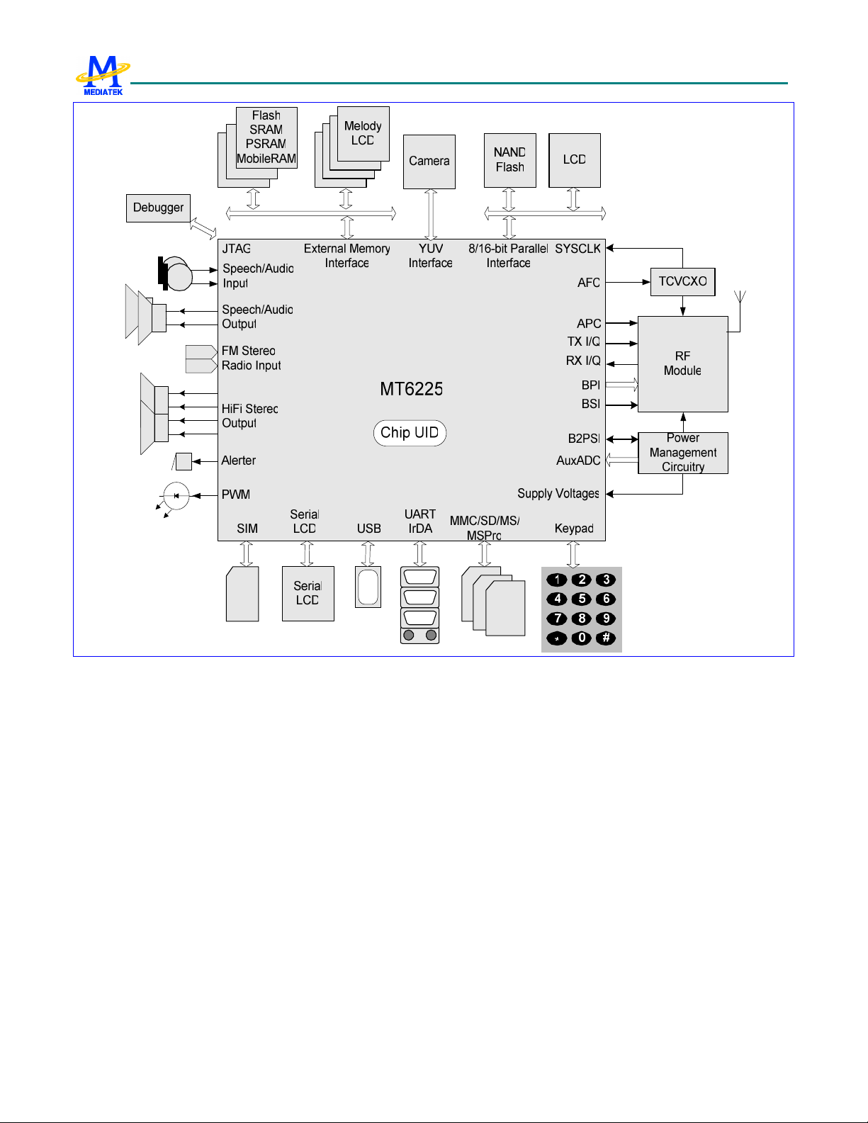
1. System Overview
The MT6225 is a highly integrated single chip soluti
GSM/GPRS phone. Based on 32-bit ARM7EJ-STM RISC
processor, MT6225 features not only high performance
GPRS Class 12 MODEM but is also designed with support
for the wireless multi-media applications, such as
advanced display engine, synthesis audio with 64-tone
polyphony, digital audio playback, Java acceleration,
MMS and etc. Additionally, MT6225 provides varieties of
advanced interfaces for functionality extensions, like
3-port external memory interface, 3-port 8/16-bit parallel
interface, NAND Flash, IrDA, USB and MMC/SD/MS/MS
Pro. The typical application can be shown as Figure 1.
Platform
MT6225 is capable of running the ARM7EJ-STM RISC
processor at up to 104 MHz, thus providing fast data
processing capabilities. In addition to the high clock
frequency, a separate CODE cache is also added to further
improve the overall system efficiency.
For large amounts of data transfer, high performance DMA
(Direct Memory Access) with hardware flow control is
implemented, which greatly enhances the data movement
speed while reducing MCU processing load.
External Memory Interface
To provide the greatest capacity for expansion and
maximum bandwidth for data intensive applications such
as multimedia features, MT6225 supports up to 3 external
state-of-the-art devices through its 8/16-bit host interface.
High performance devices such as Mobile RAM and
Cellular RAM are supported for maximum bandwidth.
Traditional devices such as burst/page mode flash, page
mode SRAM, and Pseudo SRAM are also supported. For
greatest compatibility, the memory interface can also be
used to connect to legacy devices such as Color/Parallel
LCD, and multi-media companion chips are all supported
through this interface. To minimize power consumption
and ensure low noise, this interface is designed for flexible
I/O voltage and allows lowering of the supply voltage
down to 1.8V. The driving strength is configurable for
signal integrity adjustment. The data bus also employs
on for
retention technology to prevent the bus from floating
during a turn over.
Multi-media Subsystem
In order to provide more flexibility and bandwidth for
multi-media products, an additional 8/16 bit parallel
interface is incorporated. This interface is designed
specially for support with Camera companion chip as well
as LCD panel. In addition, MT6225 has camera YUV
interface that can connect to CMOS sensor of resolution up
to VGA. Moreover, it can connect NAND flash device to
provide a solution for multi-media data storage. For
running multi-media application faster, MT6225 integrates
also several hardware-based engines. With hardware based
Resizer and advanced display engine, it can display and
combine arbitrary size of images with up to 4 blending
layers.
User Interface
For user interactions, the MT6225 brings together all
necessary peripheral blocks for multi-media GSM/GPRS
phone. It comprises the Keypad Scanner with capability of
multiple key pressing, SIM Controller, Alerter, Real Time
Clock, PWM, Serial LCD Controller and General Purpose
Programmable I/Os. For connectivity and data storage, the
MT6225 consists of UART, IrDA, USB 1.1 Slave, SDIO
and MMC/SD/MS/MS Pro.
Audio Interface
Using a highly integrated mixed-signal Audio Front-End,
the MT6225 architecture allows for easy audio interfacing
with direct connection to the audio transducers. The audio
interface integrates D/A and A/D Converters for Voice
band, as well as high resolution Stereo D/A Converters for
Audio band. In addition, MT6225 also provides Stereo
Input and Analog Mux.
MT6225 supports AMR codec to adaptively optimize
speech and audio quality. Moreover, HE-AAC codec is
implemented to deliver CD-quality audio at low bit rates.
Overall, MT6225’s audio features provide a rich platform
for multi-media applications.
6/377 MediaTek Inc. Confidential

MT6225 GSM/GPRS Baseband Processor Data Sheet Revision 1.00
Radio Interface
MT6225 integrates a mixed-signal Baseband front-end in
order to provide a well-organized radio interface with
flexibility for efficient customization. It contains gain and
offset calibration mechanisms, and filters with
programmable coefficients for comprehensive
compatibility control on RF modules. This approach also
allows the usage of a high resolution D/A Converter for
controlling VCXO or crystal, thus reducing the need for
expensive TCVCXO. MT6225 achieves great MODEM
performance by utilizing 14-bit high resolution A/D
Converter in the RF downlink path. Furthermore, to reduce
the need for extra external current-driving component, the
driving strength of some BPI outputs is designed to be
configurable.
Debug Function
The JTAG interface enables in-circuit debugging of
software program with the ARM7EJ-S core. With this
standardized debugger interface, the MT6225 provides
developers with a wide set of options for choosing ARM
development kits from supports of thirty parties. For
security reason, JTAG interface can be disabled by
programming internal OTP (one-time programmable) fuse.
Power Management
The MT6225 offers various low-power features to help
reduce system power consumption. These features include
Pause Mode of 32KHz clocking at Standby State, Power
Down Mode for individual peripherals, and Processor
Sleep Mode. In addition, MT6225 is also fabricated in
advanced low leakage CMOS process, hence providing an
overall ultra low leakage solution.
Package
The MT6225 device is offered in a 12mm×12mm, 264-ball,
0.65 mm pitch, TFBGA package.
7/377 MediaTek Inc. Confidential
MT6225 GSM/GPRS Baseband Processor Data Sheet Revision 1.00
Figure 1 Typical application of MT6225
8/377 MediaTek Inc. Confidential

MT6225 GSM/GPRS Baseband Processor Data Sheet Revision 1.00
1.1 Platform Feature
General
Integrated voice-band, audio-band and base-band
TFBGA 12mm×12mm, 264-ball, 0.65 mm pitch
MCU Subsystem
ARM7EJ-S 32-bit RISC processor
High performance multi-layer AMBA bus
Java hardware acceleration for fast Java-based
ARM7EJ-S Operating frequency: 26/52/104 MHz
Dedicated DMA bus
14 DMA channels
48K Bytes on-chip SRAM
72K Bytes MCU dedicated Tightly Coupled
16K Bytes Code cache
On-chip boot ROM for Factory Flash
Watchdog timer for system crash recovery
2 sets of General Purpose Timer
Circuit Switch Data coprocessor
Division coprocessor
analog front ends
package
g
ames and applets
M
emory
Programming
Industry standard Parallel LCD Interface
Supports multi-media companion chips with 8/16
its data width
b
Flexible I/O voltage of 1.8V ~ 2.8V for memory
interface
Configurable driving strength for memory
interface
User Interfaces
6-row × 7-column keypad controller with
hardware scanner
Supports multiple key presses for gaming
SIM/USIM Controller with hardware T=0/T=1
protocol control
Real Time Clock (RTC) operating with a separate
p
ower supply
General Purpose I/Os (GPIOs)
2 Sets of Pulse Width Modulation (PWM) Output
Alerter Output with Enhanced PWM or PDM
4~10 external interrupt lines
Connectivity
3 UARTs with hardware flow control and speed up
t
o 921600 bps
IrDA modulator/demodulator with hardware
framer supports SIR mode of operation
External Memory Interface
Supports up to 3 external devices
Supports 8-bit or 16-bit memory components with
maximum size of up to 64M Bytes each
Supports Mobile RAM and Cellular RAM
Supports Flash and SRAM with Page Mode or
B
urst Mode
Supports Pseudo SRAM
9/377 MediaTek Inc. Confidential
Full-speed USB 1.1 Device controller
Multi Media Card/Secure Digital Memory
Card/Memory Stick/Memory Stick Pro host
controller
Supports SDIO interface for SDIO peripherals as
w
ell as WIFI connectivity
DAI/PCM and I2S interface for Audio application
Security

MT6225 GSM/GPRS Baseband Processor Data Sheet Revision 1.00
Supports security key for code protection
143-bit unique/secret chip ID
Power Management
Power Down Mode for analog and digital circuits
Processor Sleep Mode
Pause Mode of 32KHz clocking at Standby State
7-channel Auxiliary 10-bit A/D Converter for
charger and battery monitoring and photo sensing
Test and Debug
Built-in digital and analog loop back modes for
both Audio and Baseband Front-End
DAI port complying with GSM Rec.11.10
JTAG port for debugging embedded MCU
10/377 MediaTek Inc. Confidential

MT6225 GSM/GPRS Baseband Processor Data Sheet Revision 1.00
1.2 MODEM Features
Radio Interface and Baseband Front End
GMSK modulator with analog I and Q channel
outputs
10-bit D/A Converter for uplink baseband I and Q
signals
14-bit high resolution A/D Converter for downlink
baseband I and Q signals
Calibration mechanism of offset and gain
m
ismatch for baseband A/D Converter and D/A
Converter
10-bit D/A Converter for Automatic Power
Control
13-bit high resolution D/A Converter for
Automatic Frequency Control
Programmable Radio RX filter
2 Channels bi-directional Baseband Serial
I
nterface (BSI) with 3-wire or 4-wire control
GSM channel coding, equalization and A5/1, A5/2
nd A5/3 ciphering
a
GPRS GEA1, GEA2 and GEA3 ciphering
Programmable GSM/GPRS Modem
Packet Switched Data with CS1/CS2/CS3/CS4
coding schemes
GSM Circuit Switch Data
GPRS Class 12
Voice Interface and Voice Front End
Two microphone inputs sharing one low noise
amplifier with programmable gain and automatic
gain control (AGC) mechanism
Voice power amplifier with programmable gain
2nd
D/A Converter for voice downlink path
order Sigma-Delta A/D Converter for voice
uplink path
10-Pin Baseband Parallel Interface (BPI) with
programmable driving strength
Multi-band support
Voice and Modem CODEC
Dial tone generation
Voice Memo
Noise Reduction
Echo Suppression / Echo Cancellation
Advanced Sidetone Oscillation Reduction
Digital sidetone generator with programmable
g
ain
Two programmable acoustic compensation filters
GSM/GPRS quad vocoders for adaptive multirate
(
AMR), enhanced full rate (EFR), full rate (FR)
and half rate (HR)
FR error concealment
Supports half-duplex hands-free operation
Compliant with GSM 03.50
11/377 MediaTek Inc. Confidential

MT6225 GSM/GPRS Baseband Processor Data Sheet Revision 1.00
1.3 Multi-Media Features
LCD/NAND Flash Interface
18-bit Parallel Interface supports 8/16 bit NAND
flash and 8/9/16/18 bit Parallel LCD
8/16 bit NAND Flash Controller with 1-bit ECC
correction for mass storages
2 Chip selects available for high-density NAND
flash device
Serial LCD Interface with 8/9 bit format support
LCD Controller
Hardware accelerated display
Supports simultaneous connection to up to 2
parallel LCD and 1 serial LCD modules
Supports format: RGB332, RGB444, RGB565,
RGB666, RGB888
Supports LCD panel maximum resolution up to
8
00x600 at 16bpp
HE-AAC decode support
Audio Interface and Audio Front End
Supports I2S interface
High resolution D/A Converters for Stereo Audio
playback
Stereo analog input for stereo audio source
Analog multiplexer for Stereo Audio
Stereo to Mono Conversion
FM radio recording
Supports hardware display rotation
Capable of combining display memories with up to
4 blending layers
Accelerated Gamma correction with
programmable gamma table.
Image Signal Processor
8 bit YUV format image input
Capable of processing image of size up to VGA
Flexible I/O voltage of 1.8V ~ 2.8V
Audio CODEC
Wavetable synthesis with up to 64 tones
Advanced stereo wavetable synthesizer
Wavetable including GM full set of 128
i
nstruments and 47 sets of percussions
PCM Playback and Record
Digital Audio Playback
12/377 MediaTek Inc. Confidential

MT6225 GSM/GPRS Baseband Processor Data Sheet Revision 1.00
1.4 General Description
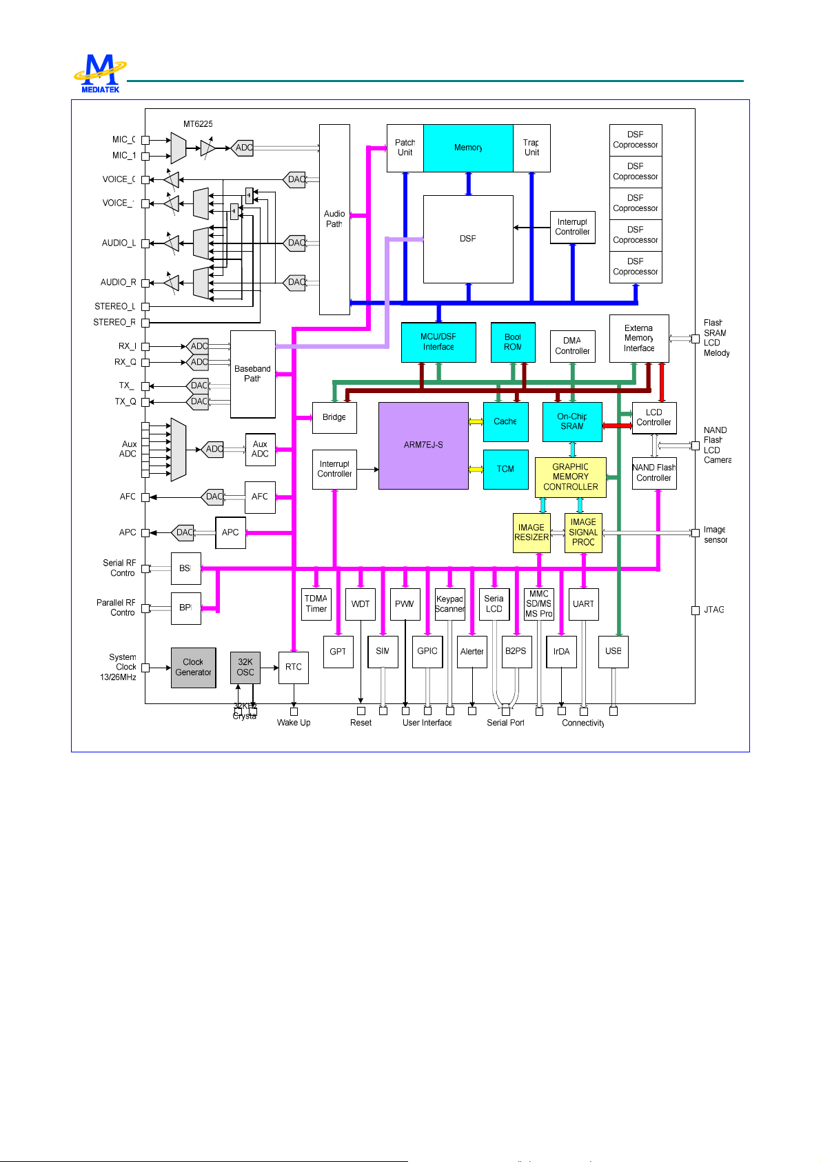
Figure 2
details the block diagram of MT6225. Based on dual-processor architecture, the major processor of MT6225
is ARM7EJ-S, which mainly runs high-level GSM/GPRS protocol software as well as multi-media applications. With
the other one is a digital signal processor corresponding for handling the low-level MODEM as well as advanced audio
functions. Except for some mixed-signal circuitries, the other building blocks in MT6225 are connected to either the
microcontroller or the digital signal processor. Specifically, MT6225 consists of the following subsystems:
Microcontroller Unit (MCU) Subsystem, including an ARM7EJ-S RISC processor and its accompanying
memory management and interrupt handling logics.
Digital Signal Processor (DSP) Subsystem, including a DSP and its accompanying memory, memory
controller, and interrupt controller.
MCU/DSP Interface, where the MCU and the DSP exchang
Microcontroller Peripherals, which include all user interface modules and RF control interface modules.
Microcontroller Coprocessors, which intend to run computing-intensive processes in place of Microcontroller.
DSP Peripherals, which are hardware accelerators for GSM/GPRS channel codec.
Multi-media Subsystem, which integrate several advanced accelerators to support multi-media applications.
Voice Front End, the data path of conveying analog s
Audio Front End, also the data path of conveying stereo audio from stereo audio source
Baseband Front End, the data path of conveying digital signal from and to analog signal of RF modules.
e hardware and software information.
peech from and to digital speech.
Timing Generator, generating the control signals related to the TDMA frame timing.
Power, Reset and Clock subsystem, managing the power, reset and clock distribution inside MT6225.
Details of the individual subsystems and blocks are described in following Chapters.
13
MT6225 GSM/GPRS Baseband Processor Data Sheet Revision 1.00
Figure 2 MT6225 block diagram.
14

MT6225 GSM/GPRS Baseband Processor Data Sheet Revision 1.00
2 Product Description
2.1 Pin Outs
One type of package for this product, TFBGA 12mm*12mm, 264-ball, 0.65 mm pitch Package, is offered.
Pin outs and the top view are illustrated in Figure 3 for this package. Outline and dimension of package is illustrated in
Figure 4, while the definition of package is shown in Table 1.
15

MT6225 GSM/GPRS Baseband Processor Data Sheet Revision 1.00
14131211106321 87 954
AVSS_
XOUT
A
XIN
B
RIN
C
AVSS_
D
RTC
JTMS
E
JRTCK
F
BSI_D
G
ATA
BSI_C
H
LK
LSCE0
J
#
K
L
M
SYSCL
PLL
AVDD_
BBWA
RTC
KEUP
JTRST
TESTM
#
JTCK
BPI_B
JTDO
BPI_B
BPI_B
US2
BPI_B
BSI_C
S0
LPCE1
LSCE1
#
LRD#LRST# LPA0
NLD14NLD13NLD12
NLD8
K
ODE
JTDI
US0
US3
US9
#
AFC
AVSS_
RFE
AFC_B
YP
PLL_O
UT
BPI_B
US1
BPI_B
US4
BPI_B
US8
LPCE0
#
LWR#
NLD15
NLD10
APC
AUXA
DIN1
AUXA
DIN3
AUXA
DIN5
BPI_B
US5
BPI_B
US7
VDD33LSDALSCK LSA0
NLD17
NLD16
NLD11NLD9NLD7
AGND
_RFE
AUXA
DIN0
AUXA
DIN2
AUXA
DIN4
AUXA
DIN6
BPI_B
US6
VDDK
VDD33
VDDK
VSS33
VDD33
VDD33
_EMI
BDLA
AU_VI
QP
N1_N
BDLA
AU_VI
QN
N0_P
AGND
BDLAI
_AFE
N
AU_VR
BDLAI
EF_PI
P
AVDD_
AVCC_
GSMR
PLL
FTX
AUX_R
AVDD_
EF
RFE
VSS33
VPP
WATC
HDOG
MT6225 TFBGA
VDD33
VSS33
_EMI
AVDD_
AFE
AU_VI
N0_P
AU_VI
N0_P
AU_VR
EF_NI
AVSS_
AFE
AVSS_
GSMR
FTX
VSS33
_USB
USB_D
P
T
op-View
VSS33
_EMI
AU_O
UT0_N
AU_O
UT0_P
AU_MI
CBIAS
_P
AU_MI
CBIAS
_N
AVDD_
BUF
AVSS_
BUF
VSS33
VSS33
USB_D
M
VSS33
_EMI
AU_M
OUTR
AVSS_
MBUF
AU_F
MINL
AU_F
MINR
AVDD_
MBUF
VDDK
AU_M
OUTL
CMDA
T0
CMDA
T1
CMDA
T2
VDD33
_CAM
VDDKVSSK
VDDK
VDD33
VDD33
VDD33
_USB
VSS33
_EMI
VDD33
_EMI
CMDA
T3
CMDA
T4
CMDA
T5
GPIO6
GPIO5
GPIO4
VDD33
VDD33
_MC
VSS33
_EMI
MCCM
0
CMDA
T6
CMDA
T7
CMHR
EF
GPIO7
KROW
1
KROW
5
KCOL3
UTXD2
SIMDA
TA
SIMRS
T
MCDA
0
ED0
CMVR
EF
CMPD
N
CMRS
T
DAIPC
MOUT
KROW
2
SIMSE
L
MCINS
MCDA
1
ED1
GPIO9
GPIO8
DAISY
NC
DAICL
K
KROW
3
SIMVC
C
MCDA
2
171615
CMPC
LK
CMMC
LK
DAIPC
MIN
KROW
0
KROW
4
KCOL2KCOL1KCOL0
URXD3UTXD3KCOL4
URXD1UTXD1URXD2
SIMCL
K
MCCKMCWP
MCDA
3
ED3ED2
A
B
C
D
E
F
G
H
J
K
L
M
NLD3
N
NRNB
P
NEW# EINT1
R
NREB
T
NCE#
U
SRCL
KENAI
SRCL
KENA
NLD5NLD4
NLD1NLD0 EINT2NLD2
GPIO0
SYSRS
T#
NLD6
NCLENALE
GPIO2
GPIO1
VSS33
VDDK
_EMI
EA23
EA19
EA20 EA16
EA24 ED12EA4
EINT0 EA25
GPIO3 EINT3
EA21 EA17
VDD33
_EMI
EA18
VSS33
_EMI
EA12
EA13
VSS33
_EMI
EA8
EA9
EA2
EA5
EA6
EPDN_
B
ECLKEA3EA7EA11EA15
EWAIT
EA1
ED4
EWR#
EUB#
ERD#ECS0#EADV#
EDCL
ECS2# ECS1#
K
ECKE ED14
ERAS# ECAS#
Figure 3 Top View of MT6225 TFBGA 12mm*12mm, 264-ball, 0.65 mm pitch Package
ED5
14131211106321 87 954 171615
ED6
ED9ED8
ED11
ED15
ELB#EA22 EA10EA14
ED7
ED10
ED13
N
P
R
T
U
16
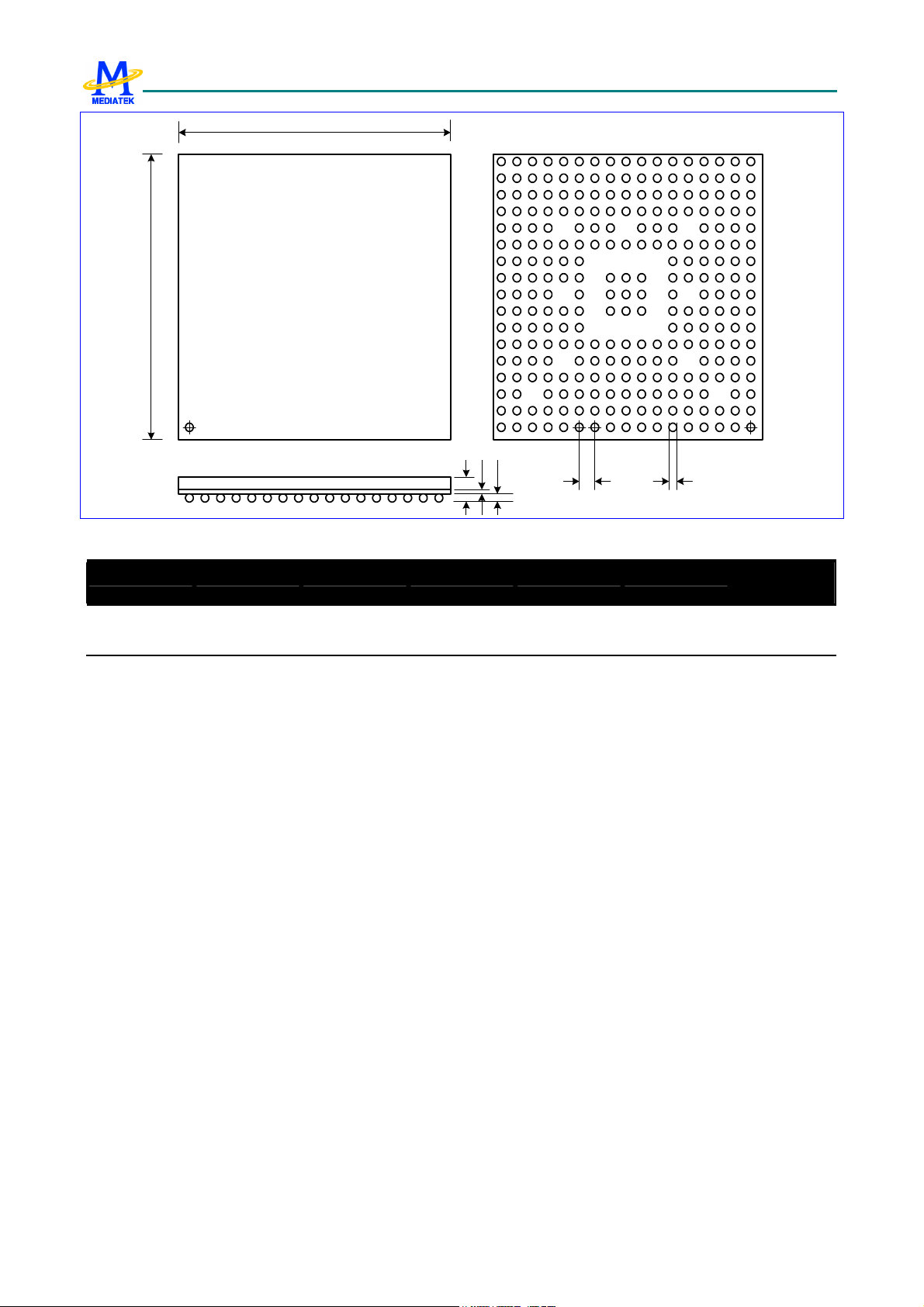
MT6225 GSM/GPRS Baseband Processor Data Sheet Revision 1.00
D
E
MT6225
Top View
(Pins Down)
A C A1
151617
MT6225
Bottem View
e b
Figure 4 Outlines and Dimension of TFBGA 12mm*12mm, 264-ball, 0.65 mm pitch Package
15 4 3 2610 9 8 711121314
A
B
C
D
E
F
G
H
J
K
L
M
N
P
R
T
U
Body Size Ball Count Ball Pitch Ball Dia. Package Thk. Stand Off Substrate
Thk.
D E N e b A (Max.) A1 C
12 12 264 0.65 0.3 1.2 0.21 0.36
Table 1 Definition of TFBGA 12mm*12mm, 264-ball, 0.65 mm pitch Package (Unit: mm)
17

MT6225 GSM/GPRS Baseband Processor Data Sheet Revision 1.00
2.2 Top Marking Definition
MT 62 25
DD DD -# # #
LL LL L
S
Figure 5 MT6225A top marking
MT6225: Part No.
DDDD: Date Code
###: Subcontractor Code
LLLLL: Lot No.
S: Special Code
18

MT6225 GSM/GPRS Baseband Processor Data Sheet Revision 1.00
2.3 DC Characteristics
2.3.1 Absolute Maximum Ratings
Prolonged exposure to absolute maximum ratings may reduce device reliability. Functional operation at these
maximum ratings is not implied.
Item Symbol Min Max Unit
IO power supply VDD33 -0.3 VDD33+0.3 V
I/O input voltage VDD33I -0.3 VDD33+0.3 V
Operating temperature Topr -20 80 Celsius
Storage temperature Tstg -55 125 Celsius
19
MT6225 GSM/GPRS Baseband Processor Data Sheet Revision 1.00
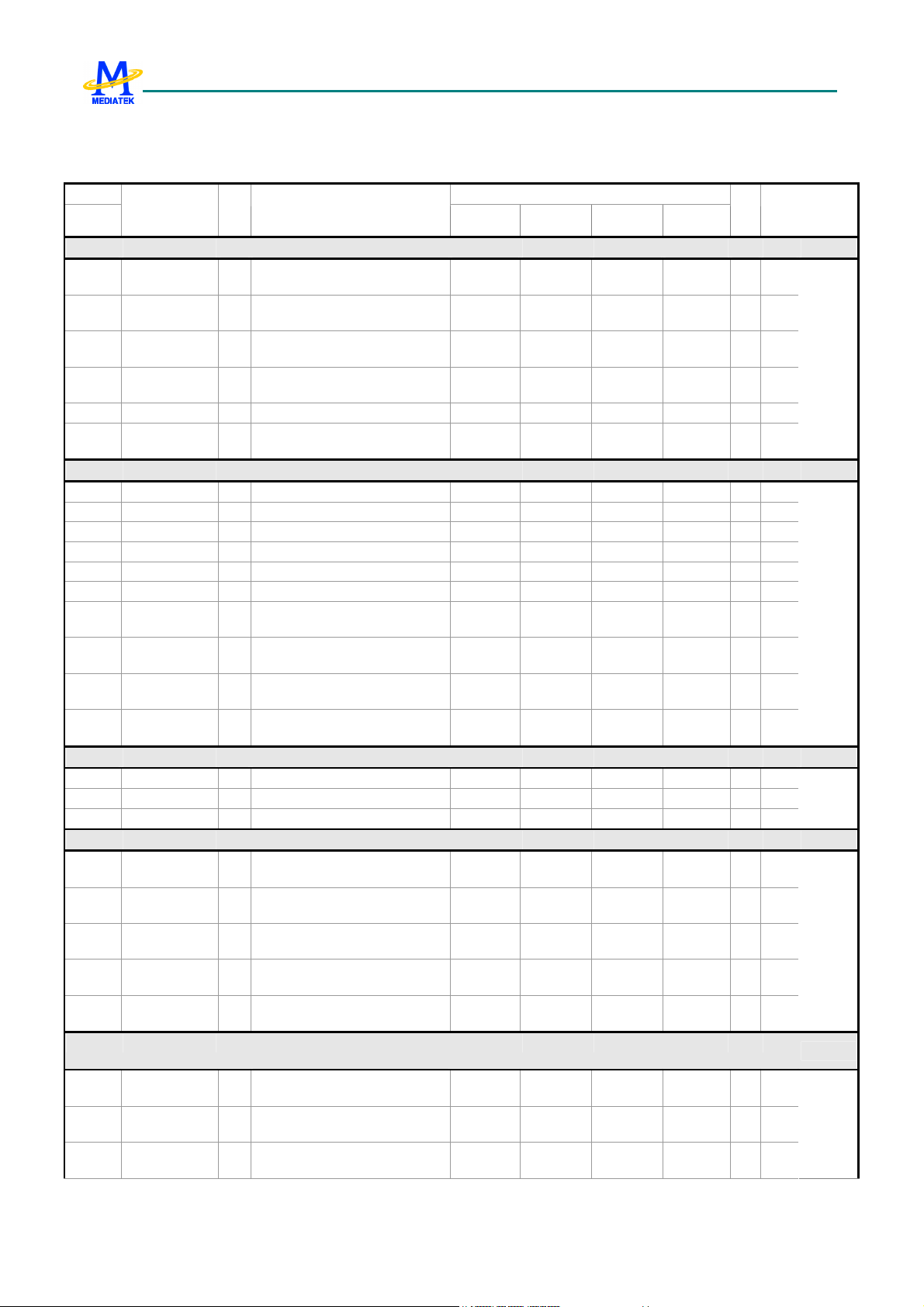
2.4 Pin Description
Ball
12X12
C2
D2
D3
E1
E2
F1
E3
E4
F2
F3
F4
F5
F6 BPI_BUS6 IO RF hard-wire control bus 6
G5 BPI_BUS7 IO RF hard-wire control bus 7
G4 BPI_BUS8 IO RF hard-wire control bus 8
G3 BPI_BUS9 IO RF hard-wire control bus 9
G2
G1
H1
H2 LSCK IO Serial display interface data
H3 LSA0 IO Serial display interface address
H4 LSDA IO Serial display interface clock
J1 LSCE0# IO Serial display interface chip
J2 LSCE1# IO Serial display interface chip
J3 LPCE1# IO Parallel display interface chip
J4
K1
Name Dir Description
JTRST#
JTCK
JTDI
JTMS
JTDO
JRTCK
BPI_BUS0
BPI_BUS1
BPI_BUS2
BPI_BUS3
BPI_BUS4
BPI_BUS5
BSI_CS0
BSI_DATA
BSI_CLK
LPCE0#
LRST#
JTAG Port
I JTAG test port reset input PD Inpu
I JTAG test port clock input PU Inpu
I JTAG test port data input PU Inpu
I JTAG test port mode switch PU Inpu
O JTAG test port data output PU 0
O JTAG test port returned clock
output
RF Parallel Control Unit
O RF hard-wire control bus 0 0
O RF hard-wire control bus 1 0
O RF hard-wire control bus 2 0
O RF hard-wire control bus 3 0
O RF hard-wire control bus 4
O RF hard-wire control bus 5
RF Serial Control Unit
O RF 3-wire interface chip select 0 0
O RF 3-wire interface data output 0
O RF 3-wire interface clock output 0
Serial LCD/PM IC Interface
output
output
output
select 0 output
select 1 output
Parallel LCD/Nand-Flash
Interface
select 1 output
O Parallel display interface chip
select 0 output
O Parallel display interface Reset
Signal
PU
Reset IO
Mode0 Mode1 Mode2 Mode3
PU 0
GPIO25
GPIO26
GPIO27
GPIO28
GPIO29
GPIO30
GPIO31
GPIO32
GPIO33
GPIO34
0
0
BPI_BUS6 PWM1 13MHz PD Inpu
BPI_BUS7 PWM2 32KHz PD Inpu
BPI_BUS8 ALERTER 26MHz PD Inpu
BPI_BUS9 BSI_CS1 PD Inpu
LSCK TDMA_CK DSP_TID0 PU Inpu
LSA0 TDMA_D1 TDTIRQ PU Inpu
LSDA TDMA_D0 TCTIRQ2 PU Inpu
LSCE0# TDMA_FS TCTIRQ1 PU Inpu
LSCE1# LPCE2# TEVTVAL PU Inpu
LPCE1# NCE1# PU Inpu
1
1
/P
D
t
t
t
t
t
t
t
t
t
t
t
t
t
t
power
VDD33
VDD33
VDD33
VDD33
VDD33
20

MT6225 GSM/GPRS Baseband Processor Data Sheet Revision 1.00
K2
K3
K4
K5 NLD17 IO Parallel LCD/Nand-Flash Data 17
L5 NLD16 IO Parallel LCD/Nand-Flash Data 16
L4
L3
L2
L1
M5
M4
M3
M2
M1
N4
N3
N2
N1
P4
P3
P2
P1 NRNB IO Nand-Flash Read/Busy Flag
R4 NCLE IO Nand-Flash Command Latch
R2 NALE IO Nand-Flash Address Latch Signal
R1 NWE# IO Nand-Flash Write Strobe
T1 NRE# IO Nand-Flash Read Strobe
U1 NCE# IO Nand-Flash Chip select output
K14
J17
J16
J15 SIMSEL IO SIM card supply power select
LRD#
LPA0
LWR#
NLD15
NLD14
NLD13
NLD12
NLD11
NLD10
NLD9
NLD8
NLD7
NLD6
NLD5
NLD4
NLD3
NLD2
NLD1
NLD0
SIMRST
SIMCLK
SIMVCC
O Parallel display interface Read
Strobe
O Parallel display interface address
output
O Parallel display interface Write
Strobe
IO Parallel LCD/Nand-Flash Data 15
IO Parallel LCD/Nand-Flash Data 14
IO Parallel LCD/Nand-Flash Data 13
IO Parallel LCD/Nand-Flash Data 12
IO Parallel LCD/Nand-Flash Data 11
IO Parallel LCD/Nand-Flash Data 10
IO Parallel LCD/Nand-Flash Data 9
IO Parallel LCD/Nand-Flash Data 8
IO Parallel LCD/Nand-Flash Data 7
IO Parallel LCD/Nand-Flash Data 6
IO Parallel LCD/Nand-Flash Data 5
IO Parallel LCD/Nand-Flash Data 4
IO Parallel LCD/Nand-Flash Data 3
IO Parallel LCD/Nand-Flash Data 2
IO Parallel LCD/Nand-Flash Data 1
IO Parallel LCD/Nand-Flash Data 0
Signal
SIM Card Interface
O SIM card reset output 0
O SIM card clock output 0
O SIM card supply power control 0
GPIO35
GPIO36
GPIO37
GPIO38
GPIO39
GPIO40
GPIO41
GPIO42
GPIO46
1
1
1
NLD17 KCOL5 VPP65 PD Inpu
t
NLD16 KCOL6 PD Inpu
t
PD Inpu
t
PD Inpu
t
PD Inpu
t
PD Inpu
t
PD Inpu
t
PD Inpu
t
PD Inpu
t
PD Inpu
t
PD Inpu
t
PD Inpu
t
PD Inpu
t
PD Inpu
t
PD Inpu
t
PD Inpu
t
PD Inpu
t
PD Inpu
t
NRNB DSP_TID1 PU Inpu
t
NCLE DSP_TID2 PD Inpu
t
NALE DSP_TID3 PD Inpu
t
NWE# DSP_TID4 PU Inpu
t
NRE# DSP_TID5 PU Inpu
t
NCE# DSP_TID6 PU Inpu
t
SIMSEL PD Inpu
VDD33
21
MT6225 GSM/GPRS Baseband Processor Data Sheet Revision 1.00
J14
T3
U4
T4
U5
G13
F13
D13
D14
B16
A16
U3
K8
U2
T2 SRCLKENAI IO External TCXO enable input
G15
G14
F17
F16
F15
F14
E17
E16
E15
E14
D17
T5
R5
P5
U6
SIMDATA
GPIO0
GPIO1
GPIO2
GPIO3
GPIO4
GPIO5
GPIO6
GPIO7
GPIO8
GPIO9
SYSRST#
WATCHDOG
SRCLKENA
KCOL4
KCOL3
KCOL2
KCOL1
KCOL0
KROW5
KROW4
KROW3
KROW2
KROW1
KROW0
EINT0
EINT1
EINT2
EINT3
IO SIM card data input/output 0
Dedicated GPIO Interface
IO General purpose input/output 0
IO General purpose input/output 1
IO General purpose input/output 2
IO General purpose input/output 3
IO General purpose input/output 4
IO General purpose input/output 5
IO General purpose input/output 6
IO General purpose input/output 7
IO General purpose input/output 8
IO General purpose input/output 9
Miscellaneous
I System reset input active low Inpu
O Watchdog reset output 1
O External TCXO enable output
active high
Keypad Interface
I Keypad column 4 PU Inpu
I Keypad column 3 PU Inpu
I Keypad column 2 PU Inpu
I Keypad column 1 PU Inpu
I Keypad column 0 PU Inpu
O Keypad row 5 0
O Keypad row 4 0
O Keypad row 3 0
O Keypad row 2 0
O Keypad row 1 0
O Keypad row 0 0
External Interrupt Interface
I External interrupt 0 PU Inpu
I External interrupt 1 PU Inpu
I External interrupt 2 PU Inpu
I External interrupt 3 PU Inpu
External Memory Interface
t
GPIO0
GPIO1
GPIO2
GPIO3
GPIO4
GPIO5
GPIO6
GPIO7
GPIO8
GPIO9
GPO0
GPIO43
22
EINT4 PU Inpu
t
EINT5 PU Inpu
t
UCTS1 EINT6 PU Inpu
t
BSI_RFIN URTS1 EINT7 PU Inpu
t
DAIRST IRDA_PDN DSP_CLK PU Inpu
t
EDICK 26MHz AHB_CLK PD Inpu
t
EDIWS 32KHz ARM_CLK PD Inpu
t
EDIDAT SLOW_C
LK
SCL PU Inpu
SDA PU Inpu
SRCLKE
NA
SRCLKE
NAI
1
PD Inpu
PD Inpu
t
t
t
t
t
t
t
t
t
t
t
t
t
t
VDD33
VDD33
_CAM
VDD33
VDD33
VDD33

MT6225 GSM/GPRS Baseband Processor Data Sheet Revision 1.00
M14
M15
M16
M17
N14
N15
N16
N17
P15
P16
P17
R16
R17
T17
U17
T16
R14
P13
R13
T15
T14
U16
P14
N12
R12
T12
P12
U14
U15
U13
T13
U12
N11
P11
R11
ED0
ED1
ED2
ED3
ED4
ED5
ED6
ED7
ED8
ED9
ED10
ED11
ED12
ED13
ED14
ED15
ERD#
EWR#
ECS0#
ECS1#
ECS2#
ELB#
EUB#
EPDN#
EADV#
EWAIT
ECLK
ERAS#
ECAS#
ECKE
EDCLK
EA1
EA2
EA3
EA4
IO External memory data bus 0 Inpu
t
IO External memory data bus 1 Inpu
t
IO External memory data bus 2 Inpu
t
IO External memory data bus 3 Inpu
t
IO External memory data bus 4 Inpu
t
IO External memory data bus 5 Inpu
t
IO External memory data bus 6 Inpu
t
IO External memory data bus 7 Inpu
t
IO External memory data bus 8 Inpu
t
IO External memory data bus 9 Inpu
t
IO External memory data bus 10 Inpu
t
IO External memory data bus 11 Inpu
t
IO External memory data bus 12 Inpu
t
IO External memory data bus 13 Inpu
t
IO External memory data bus 14 Inpu
t
IO External memory data bus 15 Inpu
t
O External memory read strobe 1
O External memory write strobe 1
O External memory chip select 0 1
O External memory chip select 1 1
O External memory chip select 2 1
O External memory lower byte
strobe
O External memory upper byte
strobe
O Power Down Control Signal for
PSRAM
O Address valid for burst mode
flash memory
I External device wait signal Inpu
O Clock for flash memory 0
O Mobile SDRAM row address
strobe
O Mobile SDRAM column address
strobe
O Mobile SDRAM clock enable 0
O Mobile SDRAM clock 0
O External memory address bus 1 0
O External memory address bus 2 0
O External memory address bus 3 0
O External memory address bus 4 0
GPO3
1
1
1
EPDN#
1
1
6.5MHz 26MHz 0*
t
VDD33
_EMI
23
MT6225 GSM/GPRS Baseband Processor Data Sheet Revision 1.00
T11
U11
P10
R10
T10
U10
P9
R9
T9
U9
P8
R8
T8
U8
P7
R7
T7
U7
P6
R6
T6
K9
K10
M13
L14
L15
L16
L17
K17
K16 MCWP IO SD Write Protect Input
K15 MCINS IO SD Card Detect Input
H17
H16
H15 URXD2 IO UART 2 receive data
H14 UTXD2 IO UART 2 transmit data
G17 URXD3 IO UART 3 receive data
G16 UTXD3 IO UART 3 transmit data
D16 DAICLK IO DAI clock output
D15 DAIPCMOUT IO DAI pcm data out
C17 DAIPCMIN IO DAI pcm data input
EA5
EA6
EA7
EA8
EA9
EA10
EA11
EA12
EA13
EA14
EA15
EA16
EA17
EA18
EA19
EA20
EA21
EA22
EA23
EA24
EA25
USB_DP
USB_DM
MCCM0
MCDA0
MCDA1
MCDA2
MCDA3
MCCK
URXD1
UTXD1
O External memory address bus 5 0
O External memory address bus 6 0
O External memory address bus 7 0
O External memory address bus 8 0
O External memory address bus 9 0
O External memory address bus 10 0
O External memory address bus 11 0
O External memory address bus 12 0
O External memory address bus 13 0
O External memory address bus 14 0
O External memory address bus 15 0
O External memory address bus 16 0
O External memory address bus 17 0
O External memory address bus 18 0
O External memory address bus 19 0
O External memory address bus 20
O External memory address bus 21
O External memory address bus 22 0
O External memory address bus 23 0
O External memory address bus 24 GPO1
O External memory address bus 25 GPO2
USB Interface
IO USB D+ Input/Output
IO USB D- Input/Output
Memory Card Interface
IO SD Command/MS Bus State
Output
IO SD Serial Data IO 0/MS Serial
Data IO
IO SD Serial Data IO 1
IO SD Serial Data IO 2
IO SD Serial Data IO 3
O SD Serial Clock/MS Serial Clock
Output
UART Interface
I UART 1 receive data
O UART 1 transmit data
Digital Audio Interface
EA24
EA25
GPIO44
GPIO45
GPIO35
GPIO36
GPIO33
GPIO34
GPIO51
GPIO52
GPIO53
MCWP PU
MCINS PU
URXD2 UCTS3 IRDA_R
UTXD2 URTS3 IRDA_T
URXD3 UCTS2 PU Inpu
UTXD3 URTS2 PU Inpu
DAICLK PU Inpu
DAIPCM
OUT
DAIPCMIN PU Inpu
26MHz 32KHz 0
32KHz 26MHz 0
XD
XD
PD Inpu
0
0
PU Inpu
t
1
PU Inpu
t
PU Inpu
t
t
t
t
t
t
VDD33
_USB
VDD33
_MC
VDD33
VDD33
24
MT6225 GSM/GPRS Baseband Processor Data Sheet Revision 1.00
sensor power down control
C16 DAISYNC IO DAI frame synchronization signal
output
C15 CMRST IO Image sensor reset signal output
B15 CMPDN IO Image
A15 CMVREF IO Sensor vertical reference signal
C14 CMHREF IO Sensor horizontal reference signal
A17
B17 CMMCLK IO Image sensor master clock output
B14 CMDAT7 IO Image sensor data input 7
A14 CMDAT6 IO Image sensor data input 6
C13 CMDAT5 IO Image sensor data input 5
B13 CMDAT4 IO Image sensor data input 4
A13 CMDAT3 IO Image sensor data input 3
D12 CMDAT2 IO Image sensor data input 2
C12 CMDAT1 IO Image sensor data input 1
B12 CMDAT0 IO Image sensor data input 0
A12
A11
C11
D11
A10
B19
C10
D10
D9
D8
B9
C9
A8
B8
A7
B7
C7
D7
CMPCLK
AU_MOUL
AU_MOUR
AU_FMINL
AU_FMINR
AU_OUT0_N
AU_OUT0_P
AU_MICBIAS
_P
AU_MICBIAS
_N
AU_VREF_N
AU_VREF_P
AU_VIN0_P
AU_VIN0_N
AU_VIN1_N
AU_VIN1_P
BDLAQP/BU
PAQP
BDLAQN/BU
PAQN
BDLAIN/BUP
AIN
BDLAIP/BUP
Image Sensor Interface
input
input
I Image sensor pixel clock input
Analog Interface
Audio analog output left channel
Audio analog output right
channel
FM radio analog input left
channel
FM radio analog input right
channel
Earphone 0 amplifier output (-)
Earphone 0 amplifier output (+)
Microphone bias supply (+)
Microphone bias supply (-)
Audio reference voltage (-)
Audio reference voltage (+)
Microphone 0 amplifier input (+)
Microphone 0 amplifier input (-)
Microphone 1 amplifier input (-)
Microphone 1 amplifier input (+)
Quadrature input (Q+) baseband
codec downlink/uplink
Quadrature input (Q-) baseband
codec downlink/uplink
In-phase input (I+) baseband
codec downlink/uplink
In-phase input (I-) baseband
GPIO54
GPIO10
GPIO11
GPIO12
GPIO13
GPIO14
GPIO15
GPIO16
GPIO17
GPIO18
GPIO19
GPIO20
GPIO21
GPIO22
DAISYNC PU Inpu
t
CMRST PD Inpu
t
CMPDN PD Inpu
t
MIRQ PU/
MFIQ PU/
Inpu
CMMCLK 26MHz 6.5MHz Outp
CMDAT7 MCDA7 Inpu
CMDAT6 MCDA6 DICK Inpu
CMDAT5 MCDA5 DID Inpu
CMDAT4 MCDA4 DIMS Inpu
CMDAT3 DSP_GPO3 TBTXEN Inpu
CMDAT2 DSP_GPO2 TBTXFS Inpu
CMDAT1 DSP_GPO1 TBRXEN PD Inpu
CMDAT0 DSP_GPO0 TBRXFS PD Inpu
PD
PD
Inpu
t
Inpu
t
t
ut
t
t
t
t
t
t
t
t
VDD33
_CAM
25
MT6225 GSM/GPRS Baseband Processor Data Sheet Revision 1.00
AIP
A5
B6
B5
C6
C5
D6
D5
E6
F7
A4
C4
A3
D4
A1
B1
C1
B3
C3
F12
G6
J6
G12
N6
M11
M6
M8
N8
M12
N7
M9
N9
M10
N10
L12
L13
APC
AUXADIN0
AUXADIN1
AUXADIN2
AUXADIN3
AUXADIN4
AUXADIN5
AUXADIN6
AUX_REF
AFC
AFC_BYP
SYSCLK
PLL_OUT
XOUT
XIN
RIN
BBWAKEUP
TESTMODE
VDDK
VDDK
VDDK
VDDK
VDDK
VDDK
VDD33_EMI
VDD33_EMI
VDD33_EMI
VDD33_EMI
VSS33_EMI
VSS33_EMI
VSS33_EMI
VSS33_EMI
VSS33_EMI
VSS33_EMI
VSS33_EMI
codec downlink/uplink
Automatic power control DAC
output
Auxiliary ADC input 0
Auxiliary ADC input 1
Auxiliary ADC input 2
Auxiliary ADC input 3
Auxiliary ADC input 4
Auxiliary ADC input 5
Auxiliary ADC input 6
Auxiliary ADC reference voltage
input
Automatic frequency control
DAC output
Automatic frequency control
DAC bypass capacitance
VCXO Interface
13MHz or 26MHz system clock
input
PLL test pin
RTC Interface
32.768 KHz crystal output
32.768 KHz crystal input
32.768 KHz crystal gain control
resistor
O Baseband power on/off control 1
I TESTMODE enable input
Supply Voltages
Supply voltage of internal logic
Supply voltage of internal logic
Supply voltage of internal logic
Supply voltage of internal logic
Supply voltage of internal logic
Supply voltage of internal logic
Supply voltage of memory
interface driver
Supply voltage of memory
interface driver
Supply voltage of memory
interface driver
Supply voltage of memory
interface driver
Ground of memory interface
driver
Ground of memory interface
driver
Ground of memory interface
driver
Ground of memory interface
driver
Ground of memory interface
driver
Ground of memory interface
driver
Ground of memory interface
driver
PD Inpu
t
AVCC_
PLL
AVDD_
RTC
Typ.
1.8V
Typ.
1.8~2.8V
26
MT6225 GSM/GPRS Baseband Processor Data Sheet Revision 1.00
K12
K13
J9
E12
H5
H6
L6
J12
H13
H12
H8
K6
M7
J10
H10
F11
J8
B2
D1
E7
A2
E11
B11
E10
F10
A9
C8
F9
A6
H9
E8
B4
F8
VDD33_USB
VDD33_MC
VSS33_USB/
MC
VDD33_CAM
VDD33
VDD33
VDD33
VDD33
VDD33
VDD33
VSS33
VSS33
VSS33
VSS33
VSS33
VSSK
VPP
AVDD_RTC
AVSS_RTC
AVCC_PLL
AVSS_PLL
AVDD_MBUF
AVSS_MBUF
AVDD_BUF
AVSS_BUF
AVDD_AFE
AGND_AFE
AVSS_AFE
AGND_RFE
AVSS_GSMR
FTX
AVDD_GSMR
FTX
AVSS_RFE
AVDD_RFE
Supply voltage of USB
transceiver
Supply voltage of memory card
interface drivers
Ground of USB/memory card
interface
Supply voltage of image sensor
interface drivers
Supply voltage for pad
Supply voltage for pad
Supply voltage for pad
Supply voltage for pad
Supply voltage for pad
Supply voltage for pad
Ground
Ground
Ground
Ground
Ground
Ground
Supply voltage for OTP
programming
Supply voltage for Real Time
Clock
Ground for Real Time Clock
Analog Supplies
Supply voltage for PLL Typ.
Ground for PLL supply
Supply Voltage for Audio band
section
GND for Audio band section
Supply voltage for voice band
transmit section
GND for voice band transmit
section
Supply voltage for voice band
receive section
GND reference voltage for voice
band section
GND for voice band receive
section
GND reference voltage for
baseband section, APC, AFC and
AUXADC
GND for baseband transmit
section
Supply voltage for baseband
transmit section
GND for baseband receive
section, APC, AFC and
AUXADC
Supply voltage for baseband
receive section, APC, AFC and
AUXADC
Typ.
3.3V
Typ.
2.8V
Typ.
Typ.
Typ.
Typ.
Typ.
Typ.
Typ.
1.8~2.8
V
Typ.
2.8V
1.8~6.5V
1.5V
1.8V
2.8V
2.8V
2.8V
2.8V
Typ.
2.8V
Table 2 Pin Descriptions (Bolded types are functions at reset)
27

MT6225 GSM/GPRS Baseband Processor Data Sheet Revision 1.00
*Note: The state of EPDN# during the system reset is low, and it changes to high after the system reset is released.
28

MT6225 GSM/GPRS Baseband Processor Data Sheet Revision 1.00
2.5 Ordering information
2.5.1 MT6225A
Part number Package Operational temperature range
MT6225A/ACS 12x12x1.2 mm 264-TFBGA -20~80°C
MT6225A/ACS-L 12x12x1.2 mm 264-TFBGA (Pb free) -20~80°C
Table 3 MT6225A ordering information
29

MT6225 GSM/GPRS Baseband Processor Data Sheet Revision 1.00
3 Micro-Controller Unit Subsystem
Figure 6 illustrates the block diagram of the Micro-Controller Unit Subsystem in MT6225. The subsystem utilizes a
main 32-bit ARM7EJ-S RISC processor, which plays the role of the main bus master controlling the whole subsystem.
All processor transactions go to code cache first. The code cache controller accesses TCM (72KB memory dedicated
to ARM7EJS core), cache memory, or bus according to the processor’s request address. If the requested content is
found in TCM or in cache, no bus transaction is required. If the code cache hit rate is high enough, bus traffic can be
effectively reduced and processor core performance maximized. In addition to the benefits of reuse of memory
contents, code cache also has a MPU (Memory Protection Unit), which allows cacheable and protection settings of
predefined regions. The contents of code cache are only accessible to MCU, and only MCU instructions are kept in
the cache memory (thus the name “code” cache).
The bus comprises of two-level system buses: Advanced High-Performance Bus (AHB) and Advanced Peripheral Bus
(APB). All bus transactions originate from bus masters, while slaves can only respond to requests from bus masters.
Before data transfer can be established, the bus master must ask for bus ownership, accomplished by request-grant
handshaking protocol between masters and arbiters.
Two levels of bus hierarchy are designed to provide optimum usage for different performance requirements.
Specifically, AHB Bus, the main system bus, is tailored toward high-speed requirements and provides 32-bit data path
with multiplex scheme for bus interconnections. The APB Bus, on the other hand, is designed to reduce interface
complexity for lower data transfer rate, and so it is isolated from high bandwidth AHB Bus by APB Bridge. APB Bus
supports 16-bit addressing and both 16-bit and 32-bit data paths. APB Bus is also optimized for minimal power
consumption by turning off the clock when there is no APB bus activity.
During operation, if the target slave is located on AHB Bus, the transaction is conducted directly on AHB Bus.
However, if the target slave is a peripheral and is attached to the APB bus, then the transaction is conducted between
AHB and APB bus through the use of APB Bridge.
The MT6225 MCU subsystem supports only memory addressing method. Therefore all components are mapped onto
the MCU 32-bit address space. A Memory Management Unit is employed to allow for a central decode scheme.
The MMU generates appropriate selection signals for each memory-addressed module on the AHB Bus.
In order to off-load the processor core, a DMA Controller is designated to act as a master and share the bus resources
on AHB Bus to do fast data movement between modules. This controller comprises thirteen DMA channels.
The Interrupt Controller provides a software interface to manipulate interrupt events. It can handle up to 32 interrupt
sources asserted at the same time. In general, it generates 2 levels of interrupt requests, FIQ and IRQ, to the processor.
A 128K Byte SRAM is provided for acting as system memory for high-speed data access. For factory programming
purpose, a Boot ROM module is used. These two modules use the same Internal Memory Controller to connect to AHB
Bus.
External Memory Interface supports both 8-bit and 16-bit devices. Since AHB Bus is 32-bit wide, all the data transfer
will be converted into several 8-bit or 16-bit cycles depending on the data width of target device. Note that, this
interface is specific to both synchronous and asynchronous components, like Flash, SRAM and parallel LCD. This
interface supports also page and burst mode type of Flash.
30
 Loading...