

MediaTek MT6223 Schematics

MT6223 GSM/GPRS
Baseband Pr ocessor
Data Sheet
Revision 2.01
Oct 05, 2007

Revision History
Revision Date Comments
1.00 Oct 26, 2006 First Release
1.01 Nov 6, 2006 Modify Pin-out, LCD interface, GPIO and analog control
1.02 Nov 17, 2006 1. Modify LCD interface
2. Modify EMI descriptions
3. Modify GPIO
4. Modify Analog front end and audio front end
1.03 Dec 1, 2006 1. Modify micro-controller subsystem descriptions.
2. Add PMU descriptions into analog front end part.
1.06 Mar 19, 2007 1. Update Baseband Front End descriptions
2. Update General Purpose IO descriptions
3. Add Efuse Controller segment
4. Update analog front end and PMU part descriptions
5. Update Auxiliary ADC segment
6. Update Automatic Frequency Control segment
7. Update Timing Generator descriptions
8. Update Software power down control
1.07 Apr 3, 2007 1. Remove NAND and memory card interface descriptions
2. Remove NiMH battry charger support in product summary section
1.08 Apr 13, 2007 1. Modify naming of external memory interface pin out
1.09 May 29,2007 1. Modify system overview descriptions
1.10 Jun 6
1.11 Jun 13
th
, 2007 1. Update information for MT6223P, including feature and part number
2. Hardware change for MT6223P’s new feature, including LCD interface change and GPIO
setting
th
, 2007 1. Correct the typo in row number of TFBGA dimension
2. BPI_BUS2 should be placed in ball number R3, and number U2 have no ball out
1.12 Jun 14th, 2007 1. Modified TFBGA diagram figure
1.13 Jun 21th, 2007 Limit the card type
1.14 Jun 26th, 2007 Reverse Aux Func. 0 and Aux Func. 1
1.15 Jun 27th, 2007 Remove serial LCD interface and EINT7 in 2.3 Pin description, MFIQ should reside at GPIO

mode 1 of GPIO52
1.16 Jul 5th, 2007 Add driving strength to BPI_BUS3 and slow-down control for wavetable, corresponding to E5
1.17 Jul 21th, 2007 Modify the BGA diagram
1.18 Aug 02th,
2007
1.19 Aug 22th,
2007
1.20 Aug 24th,
2007
2.00 Aug 30th,
2007
2.01 Oct 4th, 2007 Correct GPIO50 definition and new electrical characteristics
Remove incorrect description about USB and other project name. Change the VRTC LDO
spec.
Remove GPIO52 mode 0 from ECS3_B. Add digital pin electrical characteristics section
Replace MIRQ at EINT2 (GPIO42)
Revised CC mode spec.

TABLE OF CONTENTS
Revision History......................................................................................................................................................................2
1. System Overview..............................................................................................................................................................6
1.1 Platform Features .....................................................................................................................................................10
1.2 MODEM Features .................................................................................................................................................... 11
1.3 Multi-Media Features ...............................................................................................................................................12
1.4 General Description.................................................................................................................................................. 13
2 Prod uct Descr i ptions.....................................................................................................................................................15
2.1 Pin Outs....................................................................................................................................................................15
2.2 Top Marking Definition............................................................................................................................................ 17
2.3 Pin Description.........................................................................................................................................................20
2.4 Digital Pin Electrical Characteristics........................................................................................................................ 31
3 Micro-Controller Unit Subsystem ................................................................................................................................31
3.1 Processor Core..........................................................................................................................................................36
3.2 Memory Management .............................................................................................................................................. 36
3.3 Bus System...............................................................................................................................................................39
3.4 Direct Memory Access .............................................................................................................................................43
3.5 Interrupt Controller...................................................................................................................................................62
3.6 External Memory Interface.......................................................................................................................................79
3.7 Internal Memory Interface........................................................................................................................................91
3.8 Alerter.......................................................................................................................................................................91
3.9 SIM Interface............................................................................................................................................................ 94
3.10 Keypad Scanner...................................................................................................................................................... 104
3.11 LCD Interface......................................................................................................................................................... 107
3.12 UART .....................................................................................................................................................................120
3.13 Auxiliary ADC Unit ............................................................................................................................................... 138
3.14 General Purpose Inputs/Outputs.............................................................................................................................141
3.15 General Purpose Timer........................................................................................................................................... 159
3.16 GPRS Cipher Unit..................................................................................................................................................163
3.17 Security Engine ......................................................................................................................................................168
3.18 Real Time Clock.....................................................................................................................................................171
3.19 Divider.................................................................................................................................................................... 179
3.20 CSD Accelerator.....................................................................................................................................................184
3.21 FCS Codec.............................................................................................................................................................. 198
3.22 EFUSE Controller (efusec).....................................................................................................................................202
4 Radio Interface Control..............................................................................................................................................203
4.1 Baseband Serial Interface....................................................................................................................................... 203
4.2 Baseband Parallel Interface .................................................................................................................................... 212
4.3 Automatic Power Control (APC) Unit ................................................................................................................... 217
4.4 Automatic Frequency Control (AFC) Unit............................................................................................................. 224
5 Baseband Front End....................................................................................................................................................228
5.1 Baseband Serial Ports............................................................................................................................................. 229
5.2 Downlink Path (RX Path)....................................................................................................................................... 232
5.3 Uplink Path (TX Path)............................................................................................................................................ 242
6 Audio Front-End..........................................................................................................................................................247
6.1 General Description................................................................................................................................................ 247
6.2 Register Definitions................................................................................................................................................ 250
6.3 DSP Register Definitions........................................................................................................................................ 256
6.4 Programming Guide ............................................................................................................................................... 260
7 Timing Generator........................................................................................................................................................261
7.1 TDMA timer........................................................................................................................................................... 261
7.2 Slow Clocking Unit................................................................................................................................................ 272
8 Power and Cl ocks........................................................................................................................................................276
8.1 Software Power Down Control...............................................................................................................................276

9 Analog Front-end & Analog Blocks...........................................................................................................................282
9.1 General Description................................................................................................................................................ 282
9.2 MCU Register Definitions......................................................................................................................................294
9.3 Programming Guide ............................................................................................................................................... 333

1. System Overview
MT6223 is an entry level chipset solution with class 12
GPRS/GSM modem. It integrates only only analog
baseband but also power management blocks into one chip
and can greatly reduce the component count and make
smaller PCB size. Besides, MT6223 is capable of SAIC
(Single Antenna Interference Cancellation) and AMR
speech. Based on 32 bit ARM7EJ-S
MT6223 provides an unprecedented platform for high
quality modem performance.
Typical application diagram is shown in Figure 1.
Platform
MT6223 runs the ARM7EJ-S
TM
52Mhz, thus providing best trade-off between system
performance and power consumption.
For large amount of data transfer, high performance DMA
(Direct Memory Access) with hardware flow control is
implemented, which greatly enhances the data movement
speed while reducing MCU processing load.
Targeted as a modem-centric platform for mobile
applications, MT6223 also provides hardware security
digital rights management for copyright protection. For
further safeguarding, and to protect manufacturer’s
development investment, hardware flash content protection
is also provided to prevent unauthorized porting of software
load.
TM
RISC processor,
RISC processor at up to
and audio synthesis technology to provide superior audio
features., e.g. MP3 ring tone. For MT6223P, MP3 player is
also supported.
Connectivity, and Storage
MT6223 supports UART as well as Bluetooth interface.
Also, necessary peripheral blocks are embedded for a voice
centric phone: Keypad Scanner with the capability to detect
multiple key presses, SIM Controller, Alerter, Real Time
Clock, PWM, Serial LCD Controller, and General Purpose
Programmable I/Os.
Furthermore, to provide more configuration and bandwidth
for display, an additional 9-bit parallel interface is
incorporated.
For MT6223P, memory card control is provided through
LCD interface, including SD and mini SD, etc. Therefore
high quality MP3 playback of 48kHz sampling with
320kbps format can be supported
Audio
Using a highly integrated mixed-signal Audio Front-End,
architecture of MT6223 allows for easy audio interfacing
with direct connection to the audio transducers. The audio
interface integrates D/A and A/D Converters for Voice band,
as well as high resolution Stereo D/A Converters for Audio
band. In addition, MT6223 also provides Stereo Input and
Analog Mux. MT6223 also supports AMR codec to
adaptively optimize speech and audio quality.
Radio
Memory
MT6223 integrates a mixed-signal Baseband front-end in
order to provide a well-organized radio interface with
MT6223 supports up to 4 external state-of-the-art devices
through its 8/16-bit host interface. Devices such as
burst/page mode Flash, page mode SRAM, and Pseudo
SRAM are supported including ADMUX type devices. For
greatest compatibility, the memory interface can also be
used to connect to legacy devices such as Color/Parallel
LCD, and multi-media companion chip are all supported
through this interface. To minimize power consumption and
ensure low noise, this interface is designed for flexible I/O
voltage and allows lowering of supply voltage down to 1.8V.
The driving strength is configurable for signal integrity
flexibility for efficient customization. It contains gain and
offset calibration mechanisms, and filters with
programmable coefficients for comprehensive compatibility
control on RF modules. This approach also allows the usage
of a high resolution D/A Converter for controlling VCXO
or crystal, thus reducing the need for expensive TCVCXO.
MT6223 achieve great MODEM performance by utilizing
14-bit high resolution A/D Converter in the RF downlink
path. Furthermore, to reduce the need for extra external
current-driving component, the driving strength of some
BPI outputs is designed to be configurable.
adjustment. The data bus also employs retention technology
to prevent the bus from floating during turn over.
Multi-media
Debug Function
The JTAG interface enables in-circuit debugging of
software program with the ARM7EJ-S core. With this
MT6223 utilize high resolution audio DAC, digital audio,
6/344 MediaTek Inc. Confidential

standardized debugging interface, MT6223 provides
developers with a wide set of options in choosing ARM
development kits from different third party vendors.
Low Power Features
MT6223 offers various low-power features to help reduce
system power consumption. These features include Pause
Mode of 32KHz clocking at Standby State, Power Down
Mode for individual peripherals, and Processor Sleep Mode.
In addition, MT6223 are also fabricated in advanced low
leakage CMOS process, hence providing an overall ultra
low leakage solution.
Power Management
MT6223 integrates all regulators that a voice-centric phone
needs. Seven LDOs optimized for Specific GSM/GPRS
baseband sub-systems are included, and a RF transceiver
needed LDO is also built-in. Besides Li-Ion battery charge
function, SIM card level shifter interface, two open-drain
output switches to control the LED and vibrator are
equipped. Other power management schemes such as
thermal overload protection, Under Voltage Lock-out
Protection (UVLO), over voltage protection and oower-on
reset and start-up timer are also MT6223 features. Besides,
3 NMOS switches controlling the RGB LEDs are also
embedded to reduce BOM coount.
Package
The MT6223 device is offered in 9mm×9mm, 224-ball, 0.5
mm pitch, TFBGA package.
7/344 MediaTek Inc. Confidential

8/344 MediaTek Inc. Confidential
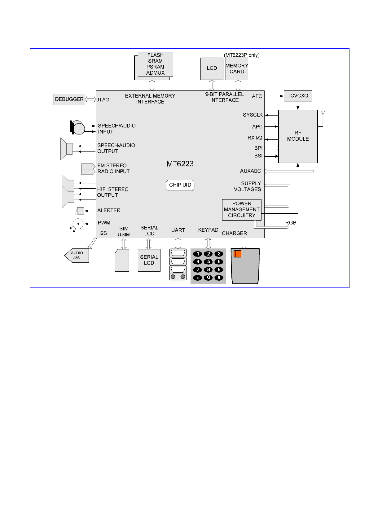
Figure 1 Typical application of MT6223.
9/344 MediaTek Inc. Confidential

1.1 Platform Features
General
z Integrated voice-band, audio-band and base-band
analog front ends
z TFBGA 9mm×9mm, 224-ball, 0.5 mm pitch
package
MCU Subsystem
z ARM7EJ-S 32-bit RISC processor
z High performance multi-layer AMBA bus
z Java hardware acceleration for fast Java-based
games and applets
z Supports multiple key presses for gaming
z SIM/USIM Controller with hardware T=0/T=1
protocol control
z Real Time Clock (RTC) operating with a separate
power supply
z General Purpose I/Os (GPIOs)
z 2 Sets of Pulse Width Modulation (PWM) Output
z Alerter Output with Enhanced PWM or PDM
z 6 external interrupt lines
Security
z Supports security key and 59 bit chip unique ID
z Operating frequency: 26/52 MHz
z Dedicated DMA bus
z 7 DMA channels
z 320K bits on-chip SRAM
z On-chip boot ROM for Factory Flash Programming
z Watchdog timer for system crash recovery
z 3 sets of General Purpose Timer
z Circuit Switch Data coprocessor
z Division coprocessor
External Memory Interface
z Supports up to 4 external devices
z Supports 8-bit or 16-bit memory components with
maximum size of up to 32M Bytes each
z Supports Flash and SRAM/PSRAM with Page
Mode or Burst Mode
z Supports ADMUX
z Industry standard 9-bit Parallel LCD Interface
z Supports multi-media companion chips with 8/16
bits data width
z Flexible I/O voltage of 1.8V ~ 2.8V for memory
interface
z Configurable driving strength for memory interface
User Interfaces
z 5-row × 7-column keypad controller with hardware
scanner
Connectivity
z 3 UARTs with hardware flow control and speed up
to 921600 bps
z DAI/PCM and I2S interface for Audio application
z Memory card interface is provided for MT6223P.
SD and MMC cards are supported
Low Power Schemes
z Power Down Mode for analog and digital circuits
z Processor Sleep Mode
z Pause Mode of 32KHz clocking at Standby State
z 3-channel Auxiliary 10-bit A/D Converter for
application usage other than battery monitoring
Power and Supply Management
z 2.8V to 5.5V Input Range
z Charger Input up to 8V
z Seven LDOs Optimized for Specific GSM
Sub-systems
z One LDO for RF transceiver
z High Operation Efficiency and Low Stand-by
Current
z Li-Ion Battery Charge function
z SIM Card Interface
z Two Open-Drain Output Switches to Control the
LED and Vibrator
z Three NMOS switches to control RGB LEDs
10/344 MediaTek Inc. Confidential

z Thermal Overload Protection
z Under Voltage Lock-out Protection
z Over Voltage Protection
z Power-on Reset and Start-up Timer
1.2 MODEM Features
Radio Interface and Baseband Front End
z GMSK modulator with analog I and Q channel
outputs
Test and Debug
z Built-in digital and analog loop back modes for
both Audio and Baseband Front-End
z DAI port complying with GSM Rec.11.10
z JTAG port for debugging embedded MCU
z 10-bit D/A Converter for uplink baseband I and Q
signals
z 14-bit high resolution A/D Converter for downlink
baseband I and Q signals
z Calibration mechanism of offset and gain mismatch
for baseband A/D Converter and D/A Converter
z 10-bit D/A Converter for Automatic Power Control
z 13-bit high resolution D/A Converter for Automatic
Frequency Control
z Programmable Radio RX filter with adaptive
bandwidth control
z Dedicated Rx filter for FB acquisition
z 2 Channels Baseband Serial Interface (BSI) with
3-wire control
z Bi-directional BSI interface. RF chip register read
access with 3-wire or 4-wire interface.
z 10-Pin Baseband Parallel Interface (BPI) with
programmable driving strength
z Multi-band support
Voice and Modem CODEC
z Dial tone generation
z Voice Memo
z Noise Reduction
z Echo Suppression
z Advanced Sidetone Oscillation Reduction
z Digital sidetone generator with programmable gain
z Two programmable acoustic compensation filters
z GSM/GPRS quad vocoders for adaptive multirate
(AMR), enhanced full rate (EFR), full rate (FR) and
half rate (HR)
z GSM channel coding, equalization and A5/1, A5/2
and A5/3 ciphering
z GPRS GEA1, GEA2 and GEA3 ciphering
11/344 MediaTek Inc. Confidential

z Programmable GSM/GPRS Modem
z GSM Circuit Switch Data
z GPRS Class 12
Voice Interface and Voice Front End
z Two microphone inputs sharing one low noise
amplifier with programmable gain and automatic
gain control (AGC) mechanism
z Voice power amplifier with programmable gain
nd
z 2
order Sigma-Delta A/D Converter for voice
uplink path
z D/A Converter for voice downlink path
z Supports half-duplex hands-free operation
z Compliant with GSM 03.50
1.3 Multi-Media Features
LCD Interface
z Dedicated Parallel Interface supports 2 external
8/9 bit Parallel Interface, and Serial interface for
LCM
z For MT6223P, memory card interface is shared
with LCD interface. And the memory card control
is available for MP3 playback
LCD Controller
z Supports simultaneous connection to up to 3
parallel LCD or 2 serial LCD modules
z Supports LCM format: RGB332, RGB444,
RGB565, RGB666, RGB888
z Supports LCD module with maximum resolution
up to 176x220 at 24bpp
z 2 layer blending
z Supports hardware display rotation for each layer
Audio CODEC
z Wavetable synthesis with up to 64 tones
z Advanced wavetable synthesizer capable of
generating simulated stereo
z Wavetable including GM full set of 128
instruments and 47 sets of percussions
z PCM Playback and Record
z Digital Audio Playback
Audio Interface and Audio Front End
z Supports I2S interface
z High resolution D/A Converters for Stereo Audio
playback
z Stereo analog input for stereo audio source
z Analog multiplexer for Stereo Audio
z FM Radio Recording
z Stereo to Mono Conversion
12/344 MediaTek Inc. Confidential

1.4 General Description
Figure 2 details the block diagram of MT6223. Based on a dual-processor architecture, MT6223 integrate both an
ARM7EJ-S core and 2 digital signal processor cores. ARM7EJ-S is the main processor that is responsible for running 2G and
2.5G protocol software. Digital signal processors handle the MODEM algorithms as well as advanced audio functions.
Except for some mixed-signal circuitries, the other building blocks in MT6223 are connected to either the microcontroller or
one of the digital signal processor.
Specifically, both MT6223 consist of the following subsystems:
z Microcontroller Unit (MCU) Subsystem - includes an ARM7EJ-S RISC processor and its accompanying memory
management and interrupt handling logics.
z Digital Signal Processor (DSP) Subsystem - includes 2 DSP cores and their accompanying memory, memory
controller, and interrupt controller.
z MCU/DSP Interface - where the MCU and the DSPs exchange hardware and software information.
z Microcontroller Peripherals - includes all user interface modules and RF control interface modules.
z Microcontroller Coprocessors - runs computing-intensive processes in place of Microcontroller.
z DSP Peripherals - hardware accelerators for GSM/GPRS/EGDE channel codec.
z Voice Front End - the data path for converting analog speech from and to digital speech.
z Audio Front End - the data path for converting stereo audio from stereo audio source
z Baseband Front End - the data path for converting digital signal from and to analog signal of RF modules.
z Timing Generator - generates the control signals related to the TDMA frame timing.
z Power, Reset and Clock subsystem - manages the power, reset, and clock distribution inside MT6223
z LDOs, Power-on sequences, swicthes and SIM level shifters.
Details of the individual subsystems and blocks are described in following Chapters.
13/344 MediaTek Inc. Confidential

VOICE_0
VOICE_1
AUDIO_L
AUDIO_R
STEREO_L
STEREO_R
TRX_Q
6 LDOs
Power
Menagement
Charger
Switches
MIC_0
MIC_1
TRX_I
Aux
ADC
AFC
APC
ADC
ADC
DAC
DAC
BB LDOs
BB LDOs
BB LDOs
RF LDO
Charger
RGB
DAC APC
ADC
+
+
Baseband
Path
32K
OSC
Aux
ADC
ADC
DAC AFC
PwrUp
Seq
DAC
DAC
DAC
RTC
Bridge
Interrupt
Controller
BPI
Audio
Path
TDMA
Timer
BSI
GPT
Patch
Unit
WDT
ARM7EJ-S
Trap
Memory
Unit
Master DSP
Boot
ROM
PWM
SIM GPIO
Share RAM
Interrupt
Controller
Coprocessors
Coprocessors
Coprocessors
MCU/DSP
Interface
MPU
SECURITY
ENGINE
Keypad
Scanner
Alerter
MT6223 : BB + PMIC SOC
Patch
DMA
UART
Unit
Trap
Unit
Interrupt
Controller
Coprocessors
Coprocessors
Coprocessors
External
Memory
Interface
Controller
Generator
Serial
LCD
Memory
On-Chip
SRAM
B2PSI
Slave DSP
Controller
LCD
Clock
Flash
SRAM
Melody
LCD
Camera BE
(MT6223P
Card I/F)
JTAG
System
Clock
13/26MHz
Serial RF
32KHz
Crystal
Parallel RF
Control
Control
User InterfaceReset
Serial Port
Connectivity
Figure 2 MT6223 block diagram.
14/344 MediaTek Inc. Confidential
2 Product Descriptions
A
2.1 Pin Outs
One type of package for this product, TFBGA 9mm * 9mm, 224-ball, 0.5mm pitch Package is offered.
Pin-outs and the top view are illustrated in Figure 3 for this package. Outline and dimension of package is illustrated in
Figure 4, while the definition of package is shown in Table 1.
1234567891011121314151617
VBAT AVBAT VBAT_RF
A
VREF VBAT VBAT ISENSE SIMIO VM VIO
B
VA RESET GATEDRV BATDET SIMRST URXD1 URXD2 URTS1_B UTXD1 EINT2 KROW0 KROW3 EA22 EA21 EA20
C
AGND RSTCAP PWRKEY LED CHRIN SIMCLK
D
AVDD_AF
E
F
G
H
J
K
L
M
N
P
R
T
U
VCTXO
E
AU_MOUTRAU_MOUT
L
AU_OUT0_NAU_OUT0_PAU_MICBI
AGND_AFEAU_MICBI
AS_N
AU_VIN0_PAU_VIN0_NAVSS_AFEAVDD_GS
AU_VIN1_NAU_VIN1_PAGND_RFEAVDD_RF
BDLAQP BDLAQN BDLAIN BDLAIP
AVSS_GS
AUXADIN0AUXADIN1AVDD_PL
MRFRX
AUXADIN
APC
2
AVSS_RF
AFC_BYP BPI_BUS5 VDD33 VDD33 DAISYNC PWM JTDI VDDK LCD_D6
E
AFC BPI_BUS0 BPI_BUS2 BPI_BUS6 BSI_DATA DAIRST ALERTER JTRST_B JTDO LCD_D7 LCD_D2
VSS_PLL BPI_BUS1 BPI_BUS4 BPI_BUS7 BSI_CS0 DAICLK DAIPCMIN
SYSCLK BPI_BUS3 BPI_BUS8 BPI_BUS9 BSI_CLK
BATSENS
VSIM AGND_RF VCORE VRF UTXD3 XOUT XIN KROW2 KCOL0 KCOL2 KCOL4
E
VRF_SEN
SE
BAT_BAC
UTXD2 VDDK UCTS1_B EINT3 EINT0 VDD33 EA19 EA18 EA17 EA16
KUP
AU_FMIN
VMSEL EA15 EA14 EA13 EA12
R
AVDD_MB
AU_FMINL
UFL
AVSS_MB
AS_P
UFL
AU_VREF
AU_VREF
_NI
_PO
MRFRX
AUX_REF VDDK
E
L
VIBRATO
R
DGND LED_R DGND DGND DGND VDDK EA5 EA4 EA3
VSS33 PGND
VSS33 VSS33
VSS33_LCDVSS33_EMIVSS33_E
SYSRST_
B
DAIPCMO
JRTCK JTCK LCD_D5 LCD_D4 LCD_D1
UT
AVDD_RT
URXD3
LED_G LED_B
VSS33_EMIVSS33_EMIVSS33_E
JTMS LCD_D8 LCD_D3
EINT1 KROW1 KROW4 KCOL1 KCOL3 EA24 EA23
C
TESTMOD
VSS33 EA2 EA1 EA0 EUB_B
E
MI
MI
VDD33_LCDVDD33_E
VDD33_E
MI
VDD33_E
MI
ELB_B ECS3_B ECS2_B ECS1_B
ECS0_B EWR_B ERD_B ED15
VDD33_E
MI
VDD33_E
MI
EA25 ED3 ED8 ED7 ED6
MI
LCD_WR_
B
LCD_RST
B
LCD_CS0
LCD_A0
_B
WATCHD
LCD_D0
OG
LCD_RD_BLCD_CS1
_B
1234567891011121314151617
SRCLKENASRCLKEN
EA11 EA10 EA9
EA8 EA7 EA6
ED14 ED13 ED12
ED11 ED10 ED9
ED4 ED5
EWAIT ED0 ED2
EADV_B ECLK ED1
A
AI
B
C
D
E
F
G
H
J
K
L
M
N
P
R
T
U
Figure 3 Top View of MT6223 TFBGA 9mm*9mm 0.5mm pitch package
15/344 MediaTek Inc. Confidential
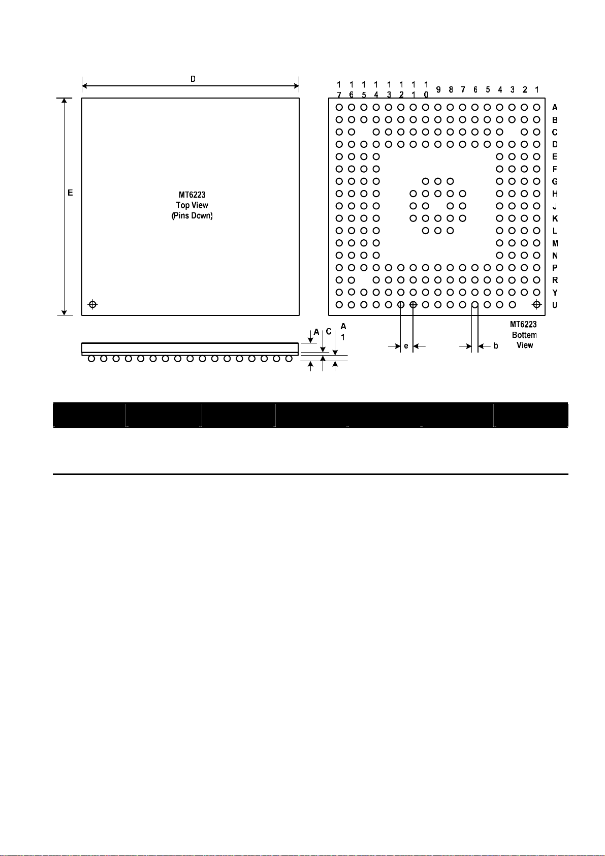
Figure 4 Outlines and Dimension of TFBGA 9mm*9mm, 224-ball, 0. 5 mm pitch Package
Body Size Ball Count Ball Pitch Ball Dia. Package Thk. Stand Off Substrate Thk.
D E N e b A (Max.) A1 C
9.0 9.0 224 0.5 0.275 1.2 0.21 0.36
Table 1 Definition of TFBGA 9mm*9mm, 224-ball, 0.5 mm pitch Package (Unit: mm)
16/344 MediaTek Inc. Confidential
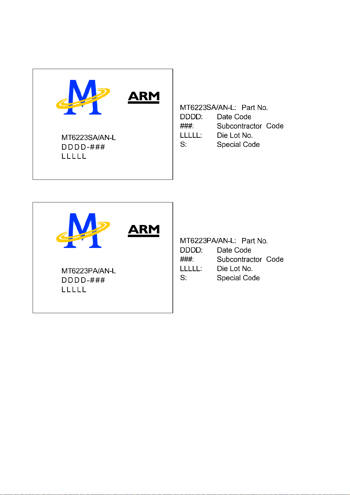
2.2 Top Marking Definition
Security version (MT6223S)
S
Memory card MP3 version (MT6223P)
S
Security, Memory card MP3 version (MT6223SP)
17/344 MediaTek Inc. Confidential
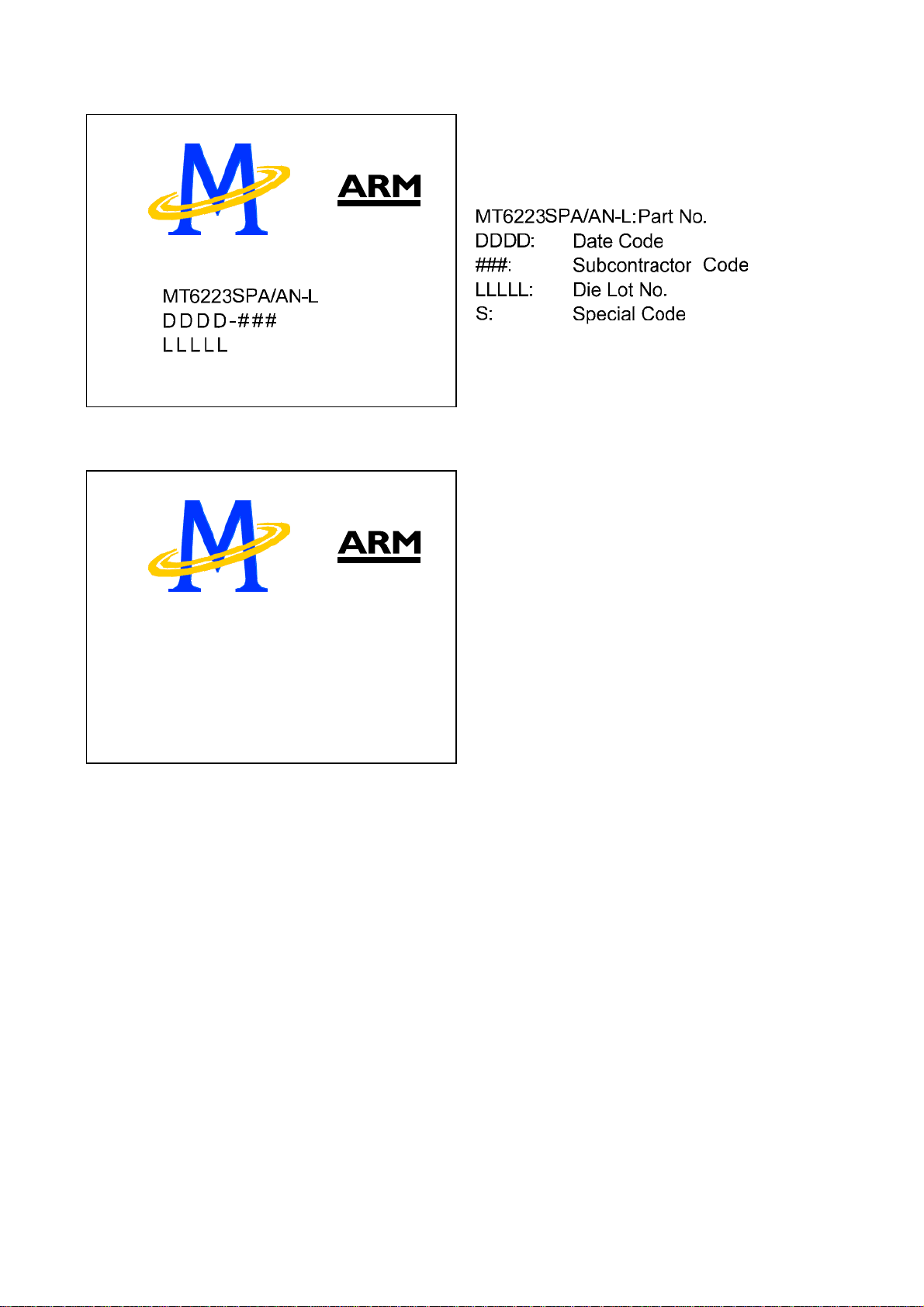
Non-security version (MT6223)
MT6223AA/AN-L
DDDD-###
LLLLL
S
MT6223AA/AN-L: Part No.
DDDD: Date Code
###: Subcontractor Code
LLLLL: Die Lot No.
S: Special Code
S
18/344 MediaTek Inc. Confidential
#

DC Characteristics
2.2.1 Absolute Maximum Ratings
Prolonged exposure to absolute maximum ratings may reduce device reliability. Functional operation at these maximum
ratings is not implied.
Item Symbol Min Max Unit
IO power supply VDD33 -0.3 VDD33+0.3 V
I/O input voltage VDD33I -0.3 VDD33+0.3 V
Operating temperature Topr -20 80 Celsius
Storage temperature Tstg -55 125 Celsius
19/344 MediaTek Inc. Confidential
2.3 Pin Description
Below pin description is identical for both MT6223.
BGA NAME Dir PIN DESCRIPTION Aux Func.0 Aux Func.1 Aux Func.2 Aux Func.3 PU/PD Reset
Analog Baseband Interface
F2 AU_MOUTL Audio analog output left channel
F1 AU_MOUTR Audio analog output right channel
E3 AU_FMINR FM radio analog input right channel
F3 AU_FMINL FM radio analog input left channel
G1 AU_OUT0_N Earphone 0 amplifier output (-)
G2 AU_OUT0_P Earphone 0 amplifier output (+)
G3 AU_MICBIAS_P Microphone bias supply (+)
H2 AU_MICBIAS_N Microphone bias supply (-)
H4 AU_VREF_PO Audio reference voltage (+)
H3 AU_VREF_NI Audio reference voltage (-)
J1 AU_VIN0_P Microphone 0 amplifier input (+)
J2 AU_VIN0_N Microphone 0 amplifier input (-)
K1 AU_VIN1_N Microphone 1 amplifier input (-)
K2 AU_VIN1_P Microphone 1 amplifier input (+)
L1 BDLAQP Quadrature (Q+) baseband codec
L2 BDLAQN Quadrature (Q-) baseband codec
L3 BDLAIN Quadrature (I-) baseband codec
L4 BDLAIP Quadrature (I+) baseband codec
N1 APC Automatic power control DAC output
M2 AUXADIN0 Auxiliary ADC input 0
M3 AUXADIN1 Auxiliary ADC input 1
N2 AUXADIN2 Auxiliary ADC input 2
N3 AUX_REF Reference voltage of Auxiliary ADC
R1 AFC Automatic frequency control DAC output
P2 AFC_BYP Automatic frequency control DAC bypass capacitance
RF control circuitry
R2 BPI_BUS0 O RF hard-wire control bus bit 0
T2 BPI_BUS1 O RF hard-wire control bus bit 1
R3 BPI_BUS2 O RF hard-wire control bus bit 2
U3 BPI_BUS3 O RF hard-wire control bus bit 3
T3 BPI_BUS4 O RF hard-wire control bus bit 4
P3 BPI_BUS5 O RF hard-wire control bus bit 5
R4 BPI_BUS6 IO RF hard-wire control bus bit 6 GPIO20 BPI_BUS6 XADMUX PD
T4 BPI_BUS7 IO RF hard-wire control bus bit 7 GPIO21 BPI_BUS7 BSI_RFIN clk_out0 PD
U4 BPI_BUS8 IO RF hard-wire control bus bit 8 GPIO22 BPI_BUS8 KCOL5 clk_out1 PU
U5 BPI_BUS9 IO RF hard-wire control bus bit 9 GPIO23 BPI_BUS9 BSI_CS1 clk_out2 PD
T5 BSI_CS0 O RF 3-wire control interface chip select 0
R5 BSI_DATA IO RF 3-wire control interface data output
U6 BSI_CLK O RF 3-wire control interface clock output
Digital Audio Interface (DAI)
T6 DAICLK IO DAI interface clock output
GPIO15
DAICLK EDICK PU
20/344 MediaTek Inc. Confidential
U7 DAIPCMOUT IO DAI PCM data output
T7 DAIPCMIN IO DAI PCM data input GPIO17 DAIPCMIN PU
R6 DAIRST IO DAI reset signal input GPIO18 DAIRST PU
P6 DAISYNC IO DAI frame synchronization input GPIO19 DAISYNC EDIWS PU
PWM Interface
R7 ALERTER IO Pulse-width modulated signal for buzzer
P7 PWM IO Pulse-width modulated signal GPIO25 PWM PD
JTAG Interface
U8 JRTCK O JTAG test port returned clock output
R8 JTRST_B I JTAG test port reset input GPIO26 JTRST_B EINT4 PD
U9 JTCK I JTAG test port clock input PU
P8 JTDI I JTAG test port data input GPIO27 JTDI EINT5 PU
T9 JTMS I JTAG test port mode switch GPIO28 JTMS EINT6 PU
R9 JTDO O JTAG test port data output
Parallel LCD Interface
T10 LCD_D8 IO Parallel display interface Data 8
R10 LCD_D7 IO Parallel display interface Data 7 GPIO1 LCD_D7 PD
P10 LCD_D6 IO Parallel display interface Data 6 GPIO2 LCD_D6 PD
U10 LCD_D5 IO Parallel display interface Data 5 GPIO3 LCD_D5 PD
U11 LCD_D4 IO Parallel display interface Data 4 GPIO4 LCD_D4 PD
T11 LCD_D3 IO Parallel display interface Data 3 GPIO5 LCD_D3 PD
R11 LCD_D2 IO Parallel display interface Data 2 GPIO6 LCD_D2 PD
U12 LCD_D1 IO Parallel display interface Data 1 GPIO7 LCD_D1 PD
T12 LCD_RSTB O Parallel display interface Reset Signal GPIO8 LCD_RSTB PU
R12 LCD_WR_B O Parallel display interface Write Strobe GPIO9 LCD_WR_B PU
U13 LCD_RD_B O Parallel display interface Read Strobe GPIO10 LCD_RD_B PU
T13 LCD_D0 IO Parallel display interface Data 0 GPIO11 LCD_D0 PD
R13 LCD_A0 O Parallel display interface address output GPIO12 LCD_A0 PU
R14 LCD_CS0_B O Parallel display interface chip select 0 output GPIO13 LCD_CS0_B PU
U14 LCD_CS1_B O Parallel display interface chip select 1 output GPIO14 LCD_CS1_B EINT7 PU
External Memory Interface
U15 EADV_B O Flash, PSRAM and CellularRAM address valid, active low
T15 EWAIT O Flash, PSRAM and CellularRAM data ready PU
U16 ECLK O Flash, PSRAM and CellularRAM clock
P13 EA25 IO External memory CRE pin
T16 ED0 IO External memory data bus 0
U17 ED1 IO External memory data bus 1
T17 ED2 IO External memory data bus 2
P14 ED3 IO External memory data bus 3
R16 ED4 IO External memory data bus 4
R17 ED5 IO External memory data bus 5
P17 ED6 IO External memory data bus 6
P16 ED7 IO External memory data bus 7
P15 ED8 IO External memory data bus 8
N17 ED9 IO External memory data bus 9
N16 ED10 IO External memory data bus 10
N15 ED11 IO External memory data bus 11
M17 ED12 IO External memory data bus 12
GPIO16
GPIO24
GPIO0
DAIPCMOUT EDIDAT PD
ALERTER PD
PU
LCD_D8 PD
21/344 MediaTek Inc. Confidential
M16 ED13 IO External memory data bus 13
M15 ED14 IO External memory data bus 14
L17 ED15 IO External memory data bus 15
L16 ERD_B O External memory read strobe, active low
L15 EWR_B O External memory write strobe, active low
L14 ECS0_B O External memory chip select 0
K17 ECS1_B O External memory chip select 1
K16 ECS2_B O External memory chip select 2
K15 ECS3_B O External memory chip select 3 MFIQ ECS3 PU
K14 ELB_B O External memory lower byte strobe
J17 EUB_B O External memory upper byte strobe
J16 EA0 O External memory address bus 0 GPIO30 EA0 EA25 PD
J15 EA1 O External memory address bus 1
J14 EA2 O External memory address bus 2
H17 EA3 O External memory address bus 3
H16 EA4 O External memory address bus 4
H15 EA5 O External memory address bus 5
G17 EA6 O External memory address bus 6
G16 EA7 O External memory address bus 7
G15 EA8 O External memory address bus 8
F17 EA9 O External memory address bus 9
F16 EA10 O External memory address bus 10
F15 EA11 O External memory address bus 11
E17 EA12 O External memory address bus 12
E16 EA13 O External memory address bus 13
E15 EA14 O External memory address bus 14
E14 EA15 O External memory address bus 15
D17 EA16 O External memory address bus 16
D16 EA17 O External memory address bus 17
D15 EA18 O External memory address bus 18
D14 EA19 O External memory address bus 19
C17 EA20 O External memory address bus 20
C16 EA21 O External memory address bus 21
C14 EA22 O External memory address bus 22
B17 EA23 O External memory address bus 23
B16 EA24 O External memory address bus 24
System Miscellaneous
J10 TESTMODE I Factory test mode enable input
T8 SYSRST_B I System reset input active low PU
T14 WATCHDOG O Watchdog reset output, active low GPIO29 WATCHDOG
A17 SRCLKENAI I External VCTCXO enable input GPIO31 SRCLKENAI PD
A16 SRCLKENA O External VCTCXO enable output active high
Keypad Interface
A15 KCOL4 I Keypad column 4
B15 KCOL3 I Keypad column 3 GPIO33 KCOL3 PU
A14 KCOL2 I Keypad column 2 GPIO34 KCOL2 PU
B14 KCOL1 I Keypad column 1 GPIO35 KCOL1 PU
A13 KCOL0 I Keypad column 0 GPIO36 KCOL0 PU
GPIO32
PD
KCOL4 PU
22/344 MediaTek Inc. Confidential
B13 KROW4 O Keypad row 4
C13 KROW3 O Keypad row 3 GPIO38 KROW3
A12 KROW2 O Keypad row 2 GPIO39 KROW2
B12 KROW1 O Keypad row 1 GPIO40 KROW1
C12 KROW0 O Keypad row 0 GPIO41 KROW0
External Interrupt Inputs
D12 EINT0 I External interrupt 0
B11 EINT1 I External interrupt 1 EINT1 PU
C11 EINT2 I External interrupt 2 GPIO42 EINT2 MIRQ BT PU
D11 EINT3 I External interrupt 3 GPIO43 EINT3 BE PU
UART
C10 UTXD1 O UART 1 transmit data
D10 UCTS1_B I UART 1 clear to send, active low GPIO45 UCTS1_B SCL PU
C9 URTS1_B O UART 1 request to send, active low GPIO46 URTS1_B SDA PU
A9 UTXD3 IO UART 3 transmit data GPIO47 UTXD3 UCTS2_B clk_out3 PU
B9 URXD3 IO UART 3 receive data GPIO48 URXD3 URTS2_B clk_out4 PU
C8 URXD2 IO UART2 receive data GPIO49 URXD2 clk_out5 PU
C7 URXD1 I UART 1 receive data GPIO50 URXD1 PU
D8 UTXD2 IO UART2 transmit data GPIO51 UTXD2 PU
Crystal and Clock Inputs
U1 SYSCLK 13MHz or 26MHz system clock input
A11 XIN 32.768 KHz crystal input
A10 XOUT 32.768 KHz crystal output
SIM Card Interface
B5 SIMIO IO SIM Data Input / Outputs
C6 SIMRST SIM card reset output
D6 SIMCLK SIM card clock output
Charger and LED Driving Interface
D5 CHRIN Charger input
C4 GATEDRV
G10 LED_B
G9 LED_G
H8 LED_R
D4 LED
G8 VIBRATOR Vibrator driving output
LDO Outputs
A5 VSIM LDO output to SIM card
A8 VRF RF LDO output
B8 VRF_SENSE RF LDO output sensing input
A7 VCORE Digital core voltage LDO output
B7 VIO Digital I/O voltage LDO output
B6 VM External memory LDO output
C1 VA Analog LDO output
E2 VCTXO Crystal or VCTCXO LDO output
PMIC Miscellaneous
A3 VBAT_RF RF used battery voltage input
B3 VBAT Battery voltage input
B2 VBAT Battery voltage input
GPIO37
GPIO44
KROW4
EINT0 PU
UTXD1 PU
23/344 MediaTek Inc. Confidential

A1 VBAT Battery voltage input
A2 AVBAT Battery voltage input
D7 BAT_BACKUP
C5 BATDET Battery detection input
A4 BATSENSE Battery sense input
B4 ISENSE Current sense input
C2 RESET Powr on reset
D2 RSTCAP Reset capacitor connection point
B1 VREF Reference voltage for PMIC
E4 VMSEL Memory supply voltage level select input
D3 PWRKEY Power key press input
Digital Power and Grounds
J8 PGND PMIC ground
H7 DGND PMIC ground
H11 DGND PMIC ground
H10 DGND PMIC ground
H9 DGND PMIC ground
K7 VSS33 Groud of chip digital part I/O circuitry
L8 VSS33 Groud of chip digital part I/O circuitry
K8 VSS33 Groud of chip digital part I/O circuitry
J11 VSS33 Groud of chip digital part I/O circuitry
J7 VSS33 Groud of chip digital part I/O circuitry
L9 VSS33_EMI Groud of external memory interface
K9 VSS33_EMI Groud of external memory interface
L10 VSS33_EMI Groud of external memory interface
K10 VSS33_EMI Groud of external memory interface
K11 VSS33_EMI Groud of external memory interface
N4 VDDK Supply voltage of digital core circuitry
P9 VDDK Supply voltage of digital core circuitry
D9 VDDK Supply voltage of digital core circuitry
H14 VDDK Supply voltage of digital core circuitry
D13 VDD33 Supply voltage of digital part I/O circuitry
P4 VDD33 Supply voltage of digital part I/O circuitry
P5 VDD33 Supply voltage of digital part I/O circuitry
P11 VDD33_LCD Supply voltage of display interface I/O circuitry
P12 VDD33_EMI Supply voltage of external memory interface
N14 VDD33_EMI Supply voltage of external memory interface
M14 VDD33_EMI Supply voltage of external memory interface
G14 VDD33_EMI Supply voltage of external memory interface
F14 VDD33_EMI Supply voltage of external memory interface
Analog Power and Grounds
K4 AVDD_RFE
F4 AVDD_MBUFL
J4 AVDD_GSMRFRX
M4 AVDD_PLL
E1 AVDD_AFE
G4 AVSS_MBUFL
T1 AVSS_PLL
24/344 MediaTek Inc. Confidential

M1 AVSS_GSMRFRX
P1 AVSS_RFE
J3 AVSS_AFE
D1 AGND
A6 AGND_RF
H1 AGND_AFE
K3 AGND_RFE
B10 AVDD_RTC Supply voltage of real time clock circuitry
Table 2 Pin Descriptions (Bolded types are functions at reset)
25/344 MediaTek Inc. Confidential
Power Description
NAME IO Supply IO GND Core Supply Core GND Remark
AU_MOUTL
AU_MOUTR
AU_FMINR
AU_FMINL
AU_OUT0_N
AU_OUT0_P
AU_MICBIAS_P
AU_MICBIAS_N
AU_VREF_PO
AU_VREF_NI
AU_VIN0_P
AU_VIN0_N
AU_VIN1_N
AU_VIN1_P
BDLAQP
BDLAQN
BDLAIN
BDLAIP
APC
AUXADIN0
AUXADIN1
AUXADIN2
AUX_REF
AFC
AFC_BYP
BPI_BUS0 VDD33 VSS33 VDDK VSSK
BPI_BUS1 VDD33 VSS33 VDDK VSSK
BPI_BUS2 VDD33 VSS33 VDDK VSSK
BPI_BUS3 VDD33 VSS33 VDDK VSSK
BPI_BUS4 VDD33 VSS33 VDDK VSSK
BPI_BUS5 VDD33 VSS33 VDDK VSSK
BPI_BUS6 VDD33 VSS33 VDDK VSSK
BPI_BUS7 VDD33 VSS33 VDDK VSSK
BPI_BUS8 VDD33 VSS33 VDDK VSSK
BPI_BUS9 VDD33 VSS33 VDDK VSSK
BSI_CS0 VDD33 VSS33 VDDK VSSK
BSI_DATA VDD33 VSS33 VDDK VSSK
BSI_CLK VDD33 VSS33 VDDK VSSK
DAICLK VDD33 VSS33 VDDK VSSK
DAIPCMOUT VDD33 VSS33 VDDK VSSK
DAIPCMIN VDD33 VSS33 VDDK VSSK
DAIRST VDD33 VSS33 VDDK VSSK
DAISYNC VDD33 VSS33 VDDK VSSK
26/344 MediaTek Inc. Confidential

ALERTER VDD33 VSS33 VDDK VSSK
PWM VDD33 VSS33 VDDK VSSK
JRTCK VDD33 VSS33 VDDK VSSK
JTRST_B VDD33 VSS33 VDDK VSSK
JTCK VDD33 VSS33 VDDK VSSK
JTDI VDD33 VSS33 VDDK VSSK
JTMS VDD33 VSS33 VDDK VSSK
JTDO VDD33 VSS33 VDDK VSSK
LCD_D8 VDD33_LCD VSS33 VDDK VSSK
LCD_D7 VDD33_LCD VSS33 VDDK VSSK
LCD_D6 VDD33_LCD VSS33 VDDK VSSK
LCD_D5 VDD33_LCD VSS33 VDDK VSSK
LCD_D4 VDD33_LCD VSS33 VDDK VSSK
LCD_D3 VDD33_LCD VSS33 VDDK VSSK
LCD_D2 VDD33_LCD VSS33 VDDK VSSK
LCD_D1 VDD33_LCD VSS33 VDDK VSSK
LCD_RSTB VDD33_LCD VSS33 VDDK VSSK
LCD_WR_B VDD33_LCD VSS33 VDDK VSSK
LCD_RD_B VDD33_LCD VSS33 VDDK VSSK
LCD_D0 VDD33_LCD VSS33 VDDK VSSK
LCD_A0 VDD33_LCD VSS33 VDDK VSSK
LCD_CS0_B VDD33_LCD VSS33 VDDK VSSK
LCD_CS1_B VDD33_LCD VSS33 VDDK VSSK
EADV_B VDD33_EMI VSS33 VDDK VSSK
EWAIT VDD33_EMI VSS33 VDDK VSSK
ECLK VDD33_EMI VSS33 VDDK VSSK
EA25 VDD33_EMI VSS33 VDDK VSSK
ED0 VDD33_EMI VSS33 VDDK VSSK
ED1 VDD33_EMI VSS33 VDDK VSSK
ED2 VDD33_EMI VSS33 VDDK VSSK
ED3 VDD33_EMI VSS33 VDDK VSSK
ED4 VDD33_EMI VSS33 VDDK VSSK
ED5 VDD33_EMI VSS33 VDDK VSSK
ED6 VDD33_EMI VSS33 VDDK VSSK
ED7 VDD33_EMI VSS33 VDDK VSSK
ED8 VDD33_EMI VSS33 VDDK VSSK
ED9 VDD33_EMI VSS33 VDDK VSSK
ED10 VDD33_EMI VSS33 VDDK VSSK
ED11 VDD33_EMI VSS33 VDDK VSSK
ED12 VDD33_EMI VSS33 VDDK VSSK
ED13 VDD33_EMI VSS33 VDDK VSSK
ED14 VDD33_EMI VSS33 VDDK VSSK
ED15 VDD33_EMI VSS33 VDDK VSSK
ERD_B VDD33_EMI VSS33 VDDK VSSK
27/344 MediaTek Inc. Confidential

EWR_B VDD33_EMI VSS33 VDDK VSSK
ECS0_B VDD33_EMI VSS33 VDDK VSSK
ECS1_B VDD33_EMI VSS33 VDDK VSSK
ECS2_B VDD33_EMI VSS33 VDDK VSSK
ECS3_B VDD33_EMI VSS33 VDDK VSSK
ELB_B VDD33_EMI VSS33 VDDK VSSK
EUB_B VDD33_EMI VSS33 VDDK VSSK
EA0 VDD33_EMI VSS33 VDDK VSSK
EA1 VDD33_EMI VSS33 VDDK VSSK
EA2 VDD33_EMI VSS33 VDDK VSSK
EA3 VDD33_EMI VSS33 VDDK VSSK
EA4 VDD33_EMI VSS33 VDDK VSSK
EA5 VDD33_EMI VSS33 VDDK VSSK
EA6 VDD33_EMI VSS33 VDDK VSSK
EA7 VDD33_EMI VSS33 VDDK VSSK
EA8 VDD33_EMI VSS33 VDDK VSSK
EA9 VDD33_EMI VSS33 VDDK VSSK
EA10 VDD33_EMI VSS33 VDDK VSSK
EA11 VDD33_EMI VSS33 VDDK VSSK
EA12 VDD33_EMI VSS33 VDDK VSSK
EA13 VDD33_EMI VSS33 VDDK VSSK
EA14 VDD33_EMI VSS33 VDDK VSSK
EA15 VDD33_EMI VSS33 VDDK VSSK
EA16 VDD33_EMI VSS33 VDDK VSSK
EA17 VDD33_EMI VSS33 VDDK VSSK
EA18 VDD33_EMI VSS33 VDDK VSSK
EA19 VDD33_EMI VSS33 VDDK VSSK
EA20 VDD33_EMI VSS33 VDDK VSSK
EA21 VDD33_EMI VSS33 VDDK VSSK
EA22 VDD33_EMI VSS33 VDDK VSSK
EA23 VDD33_EMI VSS33 VDDK VSSK
EA24 VDD33_EMI VSS33 VDDK VSSK
TESTMODE VDD33 VSS33 VDDK VSSK
SYSRST_B VDD33 VSS33 VDDK VSSK
WATCHDOG VDD33_EMI VSS33 VDDK VSSK
SRCLKENAI VDD33 VSS33 VDDK VSSK
SRCLKENA VDD33 VSS33 VDDK VSSK
KCOL4 VDD33 VSS33 VDDK VSSK
KCOL3 VDD33 VSS33 VDDK VSSK
KCOL2 VDD33 VSS33 VDDK VSSK
KCOL1 VDD33 VSS33 VDDK VSSK
KCOL0 VDD33 VSS33 VDDK VSSK
KROW4 VDD33 VSS33 VDDK VSSK
KROW3 VDD33 VSS33 VDDK VSSK
KROW2 VDD33 VSS33 VDDK VSSK
KROW1 VDD33 VSS33 VDDK VSSK
28/344 MediaTek Inc. Confidential
KROW0 VDD33 VSS33 VDDK VSSK
EINT0 VDD33 VSS33 VDDK VSSK
EINT1 VDD33 VSS33 VDDK VSSK
EINT2 VDD33 VSS33 VDDK VSSK
EINT3 VDD33 VSS33 VDDK VSSK
UTXD1 VDD33 VSS33 VDDK VSSK
UCTS1_B VDD33 VSS33 VDDK VSSK
URTS1_B VDD33 VSS33 VDDK VSSK
UTXD3 VDD33 VSS33 VDDK VSSK
URXD3 VDD33 VSS33 VDDK VSSK
URXD2 VDD33 VSS33 VDDK VSSK
URXD1 VDD33 VSS33 VDDK VSSK
UTXD2 VDD33 VSS33 VDDK VSSK
SYSCLK AVDD_PLL AVSS_PLL AVDD_PLL AVSS_PLL
XIN AVDD_RTC AVSS_RTC AVDD_RTC AVSS_RTC
XOUT AVDD_RTC AVSS_RTC AVDD_RTC AVSS_RTC
SIMIO VSIM
SIMRST VSIM
SIMCLK VSIM
CHRIN
GATEDRV
LED_B
LED_G
LED_R
LED
VIBRATOR
VSIM 3.3/1.8V
VRF 2.8V
VRF_SENSE
VCORE 1.8/1.5V
VIO 2.8V
VM 2.8/1.8V
VA 2.8V
VCTXO 2.8V
VBAT_RF
VBAT
VBAT
VBAT
AVBAT
BAT_BACKUP
BATDET
29/344 MediaTek Inc. Confidential

BATSENSE
ISENSE
RESET
RSTCAP
VREF
VMSEL
PWRKEY
PGND
DGND
DGND
DGND
DGND
VSS33
VSS33
VSS33
VSS33
VSS33
VSS33_EMI
VSS33_EMI
VSS33_EMI
VSS33_EMI
VSS33_EMI
VDDK TYP 1.8V
VDDK TYP 1.8V
VDDK TYP 1.8V
VDDK TYP 1.8V
VDD33 TYP 2.8V
VDD33 TYP 2.8V
VDD33 TYP 2.8V
VDD33_LCD 2.8V/1.8V
VDD33_EMI 2.8V/1.8V
VDD33_EMI 2.8V/1.8V
VDD33_EMI 2.8V/1.8V
VDD33_EMI 2.8V/1.8V
VDD33_EMI 2.8V/1.8V
AVDD_RFE
AVDD_MBUFL
AVDD_GSMRFRX
AVDD_PLL
AVDD_AFE
AVSS_MBUFL
AVSS_PLL
AVSS_GSMRFRX
AVSS_RFE
AVSS_AFE
AGND
30/344 MediaTek Inc. Confidential
 Loading...