

MediaTek MT6219 Schematics

MT6219 GSM/GPRS Baseband
Processor Data Sheet
Revision 1.01
Feb 11 , 2004

MT6219 GSM/GPRS Baseband Processor Data Sheet Revision 1.01
Revision History
Revision Date Comments
1.00 Feb 02, 2004 First Release
1.01 Feb 11, 2004 Analog Front-end Interface>AFE_AAC_CON register definition corrected.
2/ 418 MediaTek Inc. Confidential

MT6219 GSM/GPRS Baseband Processor Data Sheet Revision 1.01
TABLE OF CONTENTS
Revision History......................................................................................................................................2
Preface......................................................................................................................................................2
1. System Overview ...............................................................................................................................2
1.1 MODEM Features .............................................................................................................................. 2
1.2 Multi-Media Features ..........................................................................................................................2
1.3 General Description ............................................................................................................................2
2 Product Description ..........................................................................................................................2
2.1 Pin Outs............................................................................................................................................2
2.2 Pin Description................................................................................................................................... 2
2.3 Power Description ..............................................................................................................................2
3 Micro-Controller Unit Subsystem...................................................................................................2
3.1 Processor Core................................................................................................................................... 2
3.2 Memory Management.......................................................................................................................... 2
3.3 Bus System................................................................ ........................................................................2
3.4 Direct Memory Access................................ ......................................................................................... 2
3.5 Interrupt Controller .............................................................................................................................2
3.6 Internal Memory Interface ....................................................................................................................2
3.7 External Memory Interface ...................................................................................................................2
4 Microcontroller Peripherals ............................................................................................................2
4.1 Pulse-Width Modulation Outputs...........................................................................................................2
4.2 Alerter................................ ................................................................................................ ..............2
4.3 SIM Interface .....................................................................................................................................2
4.4 Keypad Scanner .................................................................................................................................2
4.5 General Purpose Inputs/Outputs................................................................ .............................................2
4.6 General Purpose Timer ........................................................................................................................2
4.7 UART ................................ ................................................................................................ ..............2
4.8 IrDA Framer ......................................................................................................................................2
4.9 Real Time Clock................................................................ .................................................................2
4.10 Auxiliary ADC Unit ............................................................................................................................2
4.11 SCCB............................................................................................................................................... 2
5 Microcontroller Coprocessors .........................................................................................................2
5.1 Divider................................................................................................ .............................................2
5.2 CSD Accelerator................................................................ .................................................................2
5.3 FCS Codec ........................................................................................................................................2
6 Multi -Media Subsystem ................................................................................................................... 2
6.1 LCD Interface ....................................................................................................................................2
6.2 JPEG Decoder.................................................................................................................................... 2
6.3 JPEG Encoder.................................................................................................................................... 2
6.4 Image Resizer ....................................................................................................................................2
6.5 NAND FLASH interface................................ ...................................................................................... 2
6.6 USB Device Controller ........................................................................................................................ 2
6.7 Memory Stick and SD Memory Card Controller ................................ .......................................................2
6.8 2D acceleration ................................................................................................ ..................................2
6.9 GIF Decoder ......................................................................................................................................2
6.10 Camera Interface ................................................................................................................................2
6.11 Image DMA ......................................................................................................................................2
6.12 Image Engine................................................................ .....................................................................2
3/ 418 MediaTek Inc. Confidential

MT6219 GSM/GPRS Baseband Processor Data Sheet Revision 1.01
6.13 MPEG-4/H.263 Video CODEC................................................................ .............................................2
7 Audio Front-end................................................................................................................................2
7.1 General Description ............................................................................................................................2
7.2 Register Definitions............................................................................................................................ 2
7.3 Programming Guide ............................................................................................................................2
8 Radio Interface Control ...................................................................................................................2
8.1 Base-band Serial Interface .................................................................................................................... 2
8.2 Base-band Parallel Interface.................................................................................................................. 2
8.3 Automatic Power Control (APC) Unit................................ .....................................................................2
8.4 Automatic Frequency Control (AFC) Unit ............................................................................................... 2
9 Baseband Front End.........................................................................................................................2
9.1 Baseband Serial Ports.......................................................................................................................... 2
9.2 Downlink Path (RX Path) .....................................................................................................................2
9.3 Uplink Path (TX Path)................................ ......................................................................................... 2
9.4 Register Definitions Summary............................................................................................................... 2
10 Timing Generator .............................................................................................................................2
10.1 TDMA timer ......................................................................................................................................2
10.2 Slow Clocking Unit................................ ............................................................................................. 2
11 Power, Clocks and Reset...................................................................................................................2
11.1 B2PSI............................................................................................................................................... 2
11.2 Clocks................................ ................................................................................................ ..............2
11.3 Reset Management.............................................................................................................................. 2
11.4 Software Power Down Control ................................................................................................ ..............2
12 Analog Front -end Interface .............................................................................................................2
12.1 General Description ............................................................................................................................2
12.2 Register Definitions............................................................................................................................ 2
4/ 418 MediaTek Inc. Confidential

MT6219 GSM/GPRS Baseband Processor Data Sheet Revision 1.01
Preface
Acronym for Register Type
R/W
RO
RC
WO
W1S
W1C
Capable of both read and write access
Read only
Read only. After reading the register bank, each bit which is HIGH(1) will be cleared to LOW(0 )
automatically.
Write only
Write only. When writing data bits to register bank, each bit which is HIGH(1) will cause the
corresponding bit to be set to 1. Data bits which are LOW(0) has no effect on the corresponding bit.
Write only. When writing data bits to register bank, each bit which is HIGH(1) will cause the
corresponding bit to be cleared to 0. Data bits which are LOW(0) has no effect on the corresponding bit.
5/ 418 MediaTek Inc. Confidential

MT6219 GSM/GPRS Baseband Processor Data Sheet Revision 1.01
6/ 418 MediaTek Inc. Confidential

MT6219 GSM/GPRS Baseband Processor Data Sheet Revision 1.01
1. System Overview
The revolutionary MT6219 is a leading edge single -chip
solution for GSM/GPRS mobile phones targeting the
emerging applications in digital audio and video. Based on
32-bit ARM7EJ-STM RISC processor, MT6219 not only
features high performance GPRS Class 12 MODEM, but
also provides comprehensive and advanced solutions for
handheld multi-media.
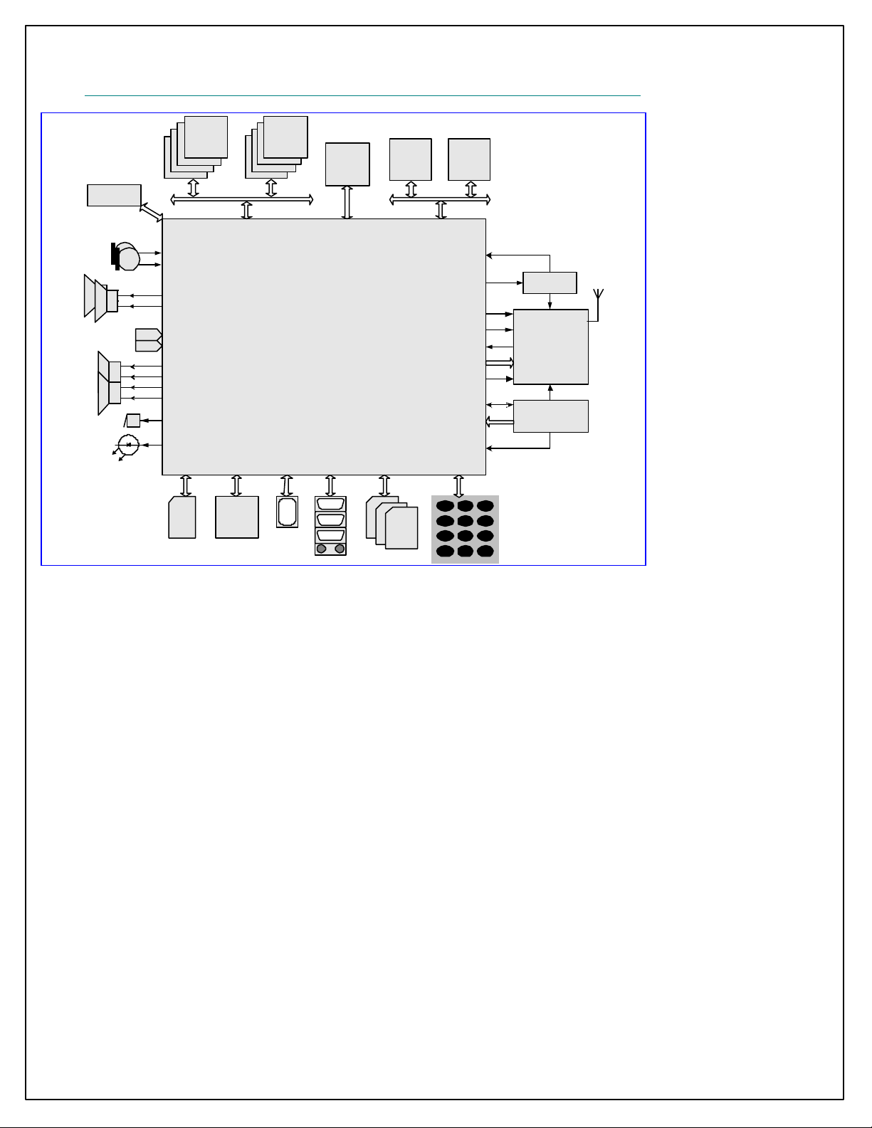
Typical application is shown in Figure 1.
Multi-media Subsystem
The MT6219 multi-media subsystem provides connection
to CMOS image sensor and supports resolution up to 1.3M
pixels. With it s advanced image signal and data processing
technology, MT6219 allows efficient processing of image
and video data. It also has built -in JPEG CODEC and
MPEG-4 CODEC, thus enabling real -time creation and
playback of high -quality images and video. In addition to
advanced image and video features, MT6219 also utilizes
high resolution DAC, digital audio, and audio synthesis
technology to provide superior audio features for all future
multi -media needs.
In order to provide more flexibility and bandwidth for
multi -media products, an additional 8-bit parallel interface
is incorporated. This interface ena bles connection to LCD
panels as well as connection to NAND flash devices to
allow for multi- media data storage capabilities.
External Memory Interface
Providing the greatest capacity for expansion, MT6219
supports up to 8 state-of-the-art devices through its 16-bit
host interface. Devices such as burst/page mode Flash,
page mode SRAM, Pseudo SRAM, Color/Parallel LCD,
and multi-media companion chip are all supported through
this interface. To minimize power consumption and ensure
low noise, this interface is designed for flexible I/O voltage
and allows lowering of supply voltage down to 1.8V. The
driving strength is configurable for signal integrity
adjustment. The data bus also employs retention
technology to prevent the bus from floating during turn
over.
7/ 418 MediaTek Inc. Confidential
User Interface
To provide complete user interface, MT6219 brings
together all the necessary peripheral blocks for
multi-media GSM /GPRS phone. The peripheral blocks
consists of the Keypad Scanner with the capability to
detect multiple key presses, SIM Controller, Alerter, Real
Time Clock, PWM, Serial LCD Controller, and General
Purpose Programmable I/Os. For connectivity and data
storage, the MT6219 supports UART, IrDA, USB 1.1
Slave and MMC/SD/MS/MS Pro. Furthermore, for large
amount of data transfer, high performance DMA (Direct
Memory Access) and hardware flow control are
implemented, which greatly enhances the performance and
reduces MCU processing load.
Audio Interface
Using a highly integrated mixed-signal Audio Front-End,
the MT6219 architecture allows for easy audio interfacing
with direct connection to the audio transducers. The audio
interface integrates D/A and A/D Converters for Voice
band, as well as high resolution Stereo D/A Converters for
Audio band. In addition, MT6219 also provides Stereo
Input and Analog Mux. Overall, MT6219’s audio features
provide a rich platform for multi-media applications.
Radio Interface
MT6219 integrates a mixed-signal Baseband front -end in
order to provide a well-organized radio interface with
flexibility for efficient customization. It contains gain and
offset calibration mechanisms, and filters with
programmable coefficients for comprehensive
compatibility control on RF modules. This approach also
allows the usage of a high resolution D/A Converter for
controlling VCXO or crystal, thus reducing the need for
expensive TCVCXO . MT6219 achieves great MODEM
performance by utilizing 14-bit high resolution A/D
Converter in the RF downlink path. Furthermore, to reduce
the need for extra external current -driving component, the
driving strength of some BPI outputs is designed to be
configurable.
Debug Function

MT6219 GSM/GPRS Baseband Processor Data Sheet Revision 1.01
The JTAG interface enables in-circuit debugging of
software program with the ARM7EJ-S core. With this
standardized debugging interface, the MT6219 provides
developers with a wide set of options in choosing ARM
development kits from different third party vendors.
Power Management
The MT6219 offers various low-power features to help
reduce system power consumption. These features include
Pause Mode of 32KHz clocking at Standby State, Power
Down Mode for individual peripherals, and Processor
Sleep Mode. In addition, MT6219 is also fabricated in
advanced low leakage CMOS process, hence providing an
overall ultra low leakage solution.
Package
The MT6219 device is offered in a 13mm×13mm, 293-ball,
0.65 mm pitch, TFBGA package.
8/ 418 MediaTek Inc. Confidential
MT6219 GSM/GPRS Baseband Processor Data Sheet Revision 1.01
FLASH
SRAM
PSRAM
DEBUGGER
JTAG
SPEECH/AUDIO
INPUT
SPEECH/AUDIO
OUTPUT
FM STEREO
RADIO INPUT
HIFI STEREO
OUTPUT
ALERTER
PWM
SIM
EXTERNAL MEMORY
INTERFACE
SERIAL
LCD
SERIAL
LCD
Figure 1 Typical application of MT6219
MELODY
LCD
USB
SENSOR
IMAGE INPUT
MT6219
UART
IRDA
CMOS
MMC/SD/MS
MSPRO
NAND
FLASH
8-BIT PARALLEL
INTERFACE
LCD
SYSCLK
AFC
APC
TX I/Q
RX I/Q
BPI
BSI
B2PSI
AUXADC
SUPPLY
VOLTAGES
KEYPAD
1 2 3
4 5 6
7 8 9
0 #
*
TCVCXO
RF
MODULE
POWER
MANAGEMENT
CIRCUITRY
9/ 418 MediaTek Inc. Confidential

MT6219 GSM/GPRS Baseband Processor Data Sheet Revision 1.01
1.1 MODEM Features
n General
l Integrated voice-band, audio -band and base-band
analog front ends
l TFBGA 13mm×13mm, 293-ball, 0.65 mm pitch
package
n MCU Subsystem
l ARM7EJ-S 32-bit RISC processor
l High performance multi-layer AMBA bus
l Java hardware acceleration for fast Java- based
games and applets
l Operating frequency: 26/52 MHz
l Dedicated DMA bus
l 14 DMA channels
l 512K Bytes zero-wait-state on-chip SRAM
l On-chip boot ROM for Factory Flash
Programming
l Watchdog timer for system crash recovery
l 2 sets of General Purpose Timer
l Circuit Switch Data coprocessor
l Division coprocessor
n External Memory Interface
l Supports up to 8 external devices
l Supports 8- bit or 16-bit memory components with
maximum size of up to 64M Bytes each
l Supports Flash and SRAM with Page Mode or
Burst Mode
l Supports Pseudo SRAM
l Industry standard Parallel LCD Interface
l Supports multi-media companion chips with 8/16
bits data width
l Flexible I/O voltage of 1.8V ~ 2.8V for memory
interface
10/418 MediaTek Inc. Confidential
l Configurable driving strength for memory
interface
n Audio and Modem CODEC
l Dial tone generation
l Voice Memo
l Noise Reduction
l Echo Suppression
l Advanced Sidetone Oscillation Reduction
l Digital sidetone generator with programmable
gain
l Two programmable acoustic compensation filters
l GSM/GPRS quad vocoders for adaptive multirate
(AMR), enhanced full rate (EFR), full rate (FR)
and half rate (HR)
l GSM channel coding, equalization and A5/1 and
A5/2 ciphering
l GPRS GEA and GEA2 ciphering
l Programmable GSM /GPRS Modem
l Packet Switched Data with CS1/CS2/CS3/CS4
coding schemes
l GSM Circuit Switch Data
l GPRS Class 12
n User Interfaces
l 6-row × 7-column keypad controller with
hardware scanner
l Supports multiple key presses for gaming
l SIM/USIM Controller with hardware T=0/T=1
protocol control
l 3 UART s with hardware flow control and speed up
to 921600 bps
l IrDA modulator/demodulator with hardware
framer

MT6219 GSM/GPRS Baseband Processor Data Sheet Revision 1.01
l Real Time Clock (RTC) operating with a separate
power supply
l Serial LCD Interface with 8/9 bit format support
l General Purpose I/Os (GPIOs)
l 2 Sets of Pulse Width Modulation (PWM) Output
l Alerter Output with Enhanced PWM or PDM
l Six external interrupt lines
n Audio Interface and Audio Front End
l Two microphone inputs sharing one low noise
amplifier with programmable gain
l Two Voice power amplifiers with programmable
gain
l 2nd order Sigma-Delta A/D Converter for voice
uplink path
l D/A Converter for voice downlink path
l Supports half- duplex hands-free operation
l Compliant with GSM 03.50
n Radio Interface and Baseband Front End
l GMSK modulator with analog I and Q channel
outputs
l 10-Pin Baseband Parallel Interface (BPI) with
programmable driving strength
l Multi-band support
n Power Management
l Power Down Mode for analog and digital circuits
l Processor Sleep Mode
l Pause Mode of 32KHz clocking at Standby State
l 7-channel Auxiliary 10-bit A/D Converter for
charger and battery monitoring and photo sensing
n Test and Debug
l Built-in digital and analog loop back modes for
both Audio and Baseband Front-End
l DAI port complying with GSM Rec.11.10
l JTAG port for debugging embedded MCU
l 10-bit D/A Converter for uplink baseband I and Q
signals
l 14-bit high resolution A/D Converter for downlink
baseband I and Q signals
l Calibration mechanism of offset and gain
mismatch for baseband A/D Converter and D/A
Converter
l 10-bit D/A Converter for Automatic Power
Control
l 13-bit high resolution D/A Converter for
Automatic Frequency Control
l Programmable Radio RX filter
l 2 Channels Baseband Serial Interface (BSI) with
3-wire control
11/418 MediaTek Inc. Confidential

MT6219 GSM/GPRS Baseband Processor Data Sheet Revision 1.01
1.2 Multi-Media Features
n LCD/NAND Flash Interface
l Dedicated 8-bit Parallel Interface, supports up to 3
external devices
l Hardware accelerated LCD Controller for display
l Dedicated LCD bus
l NAND Flash Controller for mass storages
n LCD Controller
l Supports simultaneous connection to up to 2
parallel LCD and 1 serial LCD panels
l Supports format: RGB332, RGB444, RGB565,
RGB666, RGB888
l Supports LCD panel maximum resolution up to
800x600 at 16bpp
l Supports hardware display rotation
l Capable of combining display memories with up to
4 blending layers
n Image Signal Processor
l 8/10 bit Bayer format image input
l Capable of processing image of size up to 1.3M
pixels
l Color Correction Matrix
l Gamma Correction
l Automatic Exposure Control
l Automatic White Balance Control
l Programmable AE/AWB windows
l Edge Enhancement Support
l Histogram Equalization Logic
l Horizontal and Vertical Sync Information on
Separate Pin
n JPEG Decoder
l ISO/IEC 10918-1 JPEG Baseline and Progressive
modes
12/418 MediaTek Inc. Confidential
l Supports all possible YUV formats, including
grayscale format
l Supports all DC/AC Huffman table parsing
l Supports all quantization table parsing
l Supports restart interval
l Supports SOS, DHT, DQT and DRI marker
parsing
l IEEE Std 1180 -1990 IDCT Standard Compliant
l Supports progressive image processing to
minimize storage space requirement
l Supports reload-able DMA for VLD stream
n JPEG Encoder
l ISO/IEC 10918 -1 JPEG baseline mode
l ISO/IEC 10918 -2 Compliance
l Supports YUV422 and grayscale formats
l Standard DC and AC Huffman tables
l Provides 4 levels of encode quality
n Image Data Processing
l High throughput hardware Resizer capable of
tailoring image to arbitrary size
l Horizontal scaling in averaging method
l Vertical scaling in bilinear method
l Simultaneous scaling for MPEG- 4 encode and
LCD display
l YUV and RGB color space conversion
l Pixel format transform
l Boundary padding
l Pixel processing: hue/saturation/intensity/color
adjustment, Gamma correction and
grayscale/invert/sepia-tone effects
l Programmable Spatial Filtering: Linear filter,
Non-linear filter and Multi-pass artistic effects

MT6219 GSM/GPRS Baseband Processor Data Sheet Revision 1.01
l Hardware accelerated im age editing
n MPEG -4/H.263 CODEC
l Hardware Video CODEC
l ISO/IEC 14496-2 simple profile:
decode @ level 0/1/2/3
encode @ level 0
l Supported visual tools for decoder: I-VOP, P -VOP,
AC/DC prediction, 4-MV, Unrestricted MV, Error
Resilience, Short Header
l Error Resilience for decoder: Slice
Resynchronization, Data Partitioning, Reversible
VLC
l Supported visual tools for encoder: I-VOP, P -VOP,
Half-pel, DC prediction, Unrestricted MV,
Reversible VLC, Short Header
l Supports encoding motion vector of range up
to –64/+63.5 pixels
l ITU-T H.263 profile 0 @ level 10
l AAC/AMR/WB-AMR audio decode support
l AMR/WB-AMR audio encode support
n 2D Accelerator
l Rectangle fill
l BitBlt: multi-BitBlt without transform, 7 rotate,
mirror (transparent) BitBlt
l Alpha blending
l Line drawing: normal lin e, dotted line
l Font caching: normal font, Italic font
l Supports 16-bpp RGB565 and 8-bpp index color
modes
l Command queue with 32 levels
n Audio CODEC
l Wavetable synthesis with up to 64 tones
l Advanced wavetable synthesizer capable of
generating simulated stereo
l Wavetable including GM full set of 128
instruments and 47 sets of percussions
l PCM Playback and Record
l Digital Audio Playback
l High resolution D/A Converters for Stereo Audio
playback
l Stereo analog input for stereo audio source
l Analog mixers for Stereo Audio
l Stereo to Mono Conversion
n Connectivity
l Full-speed USB 1.1 Device
l Multi Media Card/Secure Digital Memory
Card/Memory Stick/Memory Stick Pro host
controller
13/418 MediaTek Inc. Confidential

MT6219 GSM/GPRS Baseband Processor Data Sheet Revision 1.01
1.3 General Description
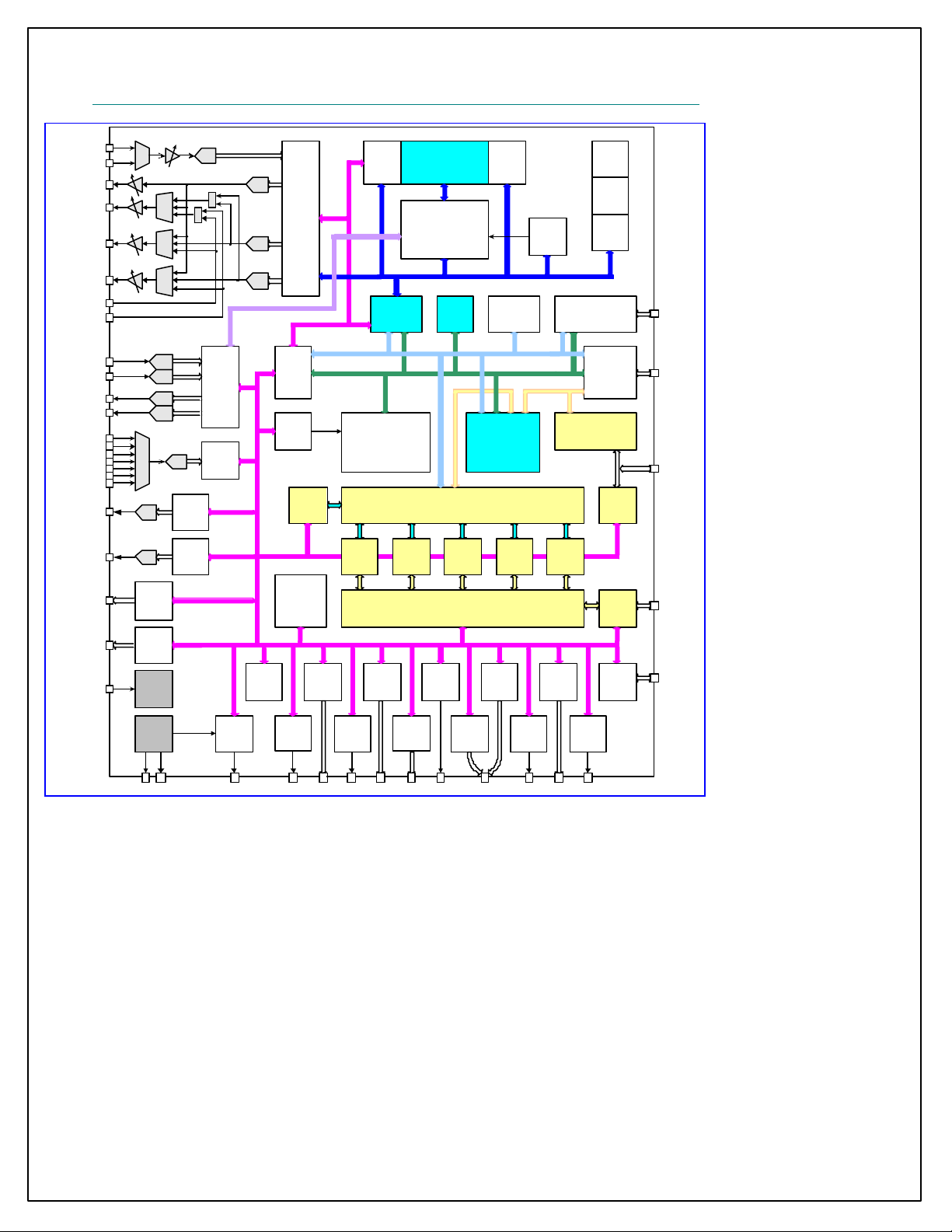
Figure 2 details the block diagram of MT6219. Based on a dual-processor architecture, MT6219 integrates both an
ARM7EJ-S core and a digital signal processor core. ARM7EJ-S is the main processor that is responsible for running
high-level GSM/GPRS protocol software as well as multi-media applications. The digital signal processor handles the
low-level MODEM as well as advanced audio functions. Except for some mixed- signal circuitries, the other building
blocks in MT6219 are connected to either the microcontroller or the digital signal processor.
Specifically, MT6219 consists of the following subsystems:
l Microcontroller Unit (MCU) Subsystem - includes an ARM7EJ-S RISC processor and its accompanying memory
management and interrupt handling logics.
l Digital Signal Processor (DSP) Subsystem - includes a DSP and its accompanying memory, memory controller,
and interrupt controller.
l MCU/DSP Interface - where the MCU and the DSP exchange hardware and software information.
l Microcontroller Peripherals - includes all user interface modules and RF control interface modules.
l Microcontroller Coprocessors - runs computing-intensive processes in place of Microcontroller.
l DSP Peripherals - hardware accelerators for GSM /GPRS channel codec.
l Multi-media Subsystem - integrates several advanced accelerators to support multi-media applications.
l Voice Front End - the data path for converting analog speech from and to digital speech.
l Audio Front End - the data path for converting stereo audio from stereo audio source
l Baseband Front End - the data path for converting digital signal from and t o analog signal of RF modules.
l Timing Generator - generat es the control signals related to the TDMA frame timing.
l Power, Reset and Clock subsystem - manages the power, reset , and clock distribution inside MT6219.
Details of the individual subsystems and blocks are described in following Chapters.
14/418 MediaTek Inc. Confidential
MT6219 GSM/GPRS Baseband Processor Data Sheet Revision 1.01
MELODY
MIC-0
MIC-1
VOICE-0
VOICE-1
AUDIO-L
AUDIO-R
STEREO-L
STEREO-R
SERIAL RF
CONTROL
PARALLEL
RF CONTROL
RX-I
RX-Q
TX-I
TX-Q
AUX
ADC
AFC
APC
ADC
ADC
DAC
DAC
ADC
DAC AFC
DAC APC
BSI
BPI
ADC
+
BASEBAND
+
PATH
AUX
ADC
DAC
DAC
DAC
AUDIO
PATH
BRIDGE
INTERRUPT
CONTROL
2D ENGINE
TDMA
TIMER
IMAGE
DMA
PATCH
UNIT
MCU/DSP
INTERFACE
ARM7EJ-S
IMAGE
ENGINE
MEMORY
DSP
BOOT
ROM
GRAPHIC MEMORY
CONTROLLER
GIF
DECODER
IMAGE RESIZER
TRAP
UNIT
CONTROL
ON-CHIP
SRAM
CODEC
DMA
JPEG
INTERRUPT
CONTROL
MPEG-4
VIDEO
CODEC
DSP CO-
PROCESSOR
DSP CO-
PROCESSOR
DSP CO-
PROCESSOR
USB
EXTERNAL
MEMORY
INTERFACE
LCD
CONTROLLER
PROCESSOR
NAND
FLASH
INTERFACE
IMAGE
SIGNAL
USB
FLASH
SRAM
PSRAM
LCD
NAND
LCD
CMOS
SENSOR
SYSTEM
CLOCK
13/26MHZ
CLOCK
GEN
32K
OSC
32KHZ CRYSTAL
GPT
RTC
WAKE UP USER INTERFACERESET
WDT
SIM GPIO
PWM
KEYPAD
SCANNER
ALERTER
SERIAL
LCD
B2PSI IRDA
MMC
SD/MS
MS PRO
CONNECTIVITYSERIAL PORT
SCCB
UART
MT6219
Figure 2 MT6219 block diagram.
15/418 MediaTek Inc. Confidential

MT6219 GSM/GPRS Baseband Processor Data Sheet Revision 1.01
2 Product Description
2.1 Pin Outs
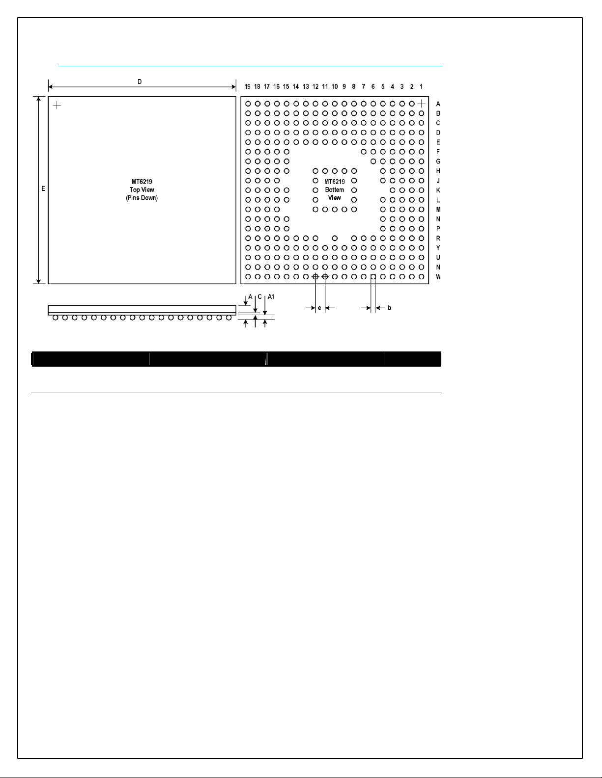
One type of package for this product, TFBGA 13mm*13mm , 293-ball, 0.65 mm pitch Package, is offered.
Pin outs and the top view are illustrated in Figure 3 for this package . Outline and dimension of package is illustrated in
Figure 4, while the definition of package is shown in Table 1.
16/418 MediaTek Inc. Confidential

MT6219 GSM/GPRS Baseband Processor Data Sheet Revision 1.01
Figure 3 Top View of MT6219 TFBGA 13mm*13mm , 293-ball, 0.65 mm pitch Package
17/418 MediaTek Inc. Confidential
MT6219 GSM/GPRS Baseband Processor Data Sheet Revision 1.01
Figure 4 Outlines and Dimension of TFBGA 13mm*1 3mm, 293-ball, 0.65 mm pitch Package
Body Size Ball Count Ball Pitch Ball Dia. Package Thk. Stand Off Substrate Thk.
D E N e b A (Max.) A1 C
13 13 293 0.65 0.35 1.4 0.3 0.36
Table 1 Definition of TFBGA 13mm*13mm, 293-ball, 0.65 mm pitch Package (Unit: mm)
18/418 MediaTek Inc. Confidential
MT6219 GSM/GPRS Baseband Processor Data Sheet Revision 1.01
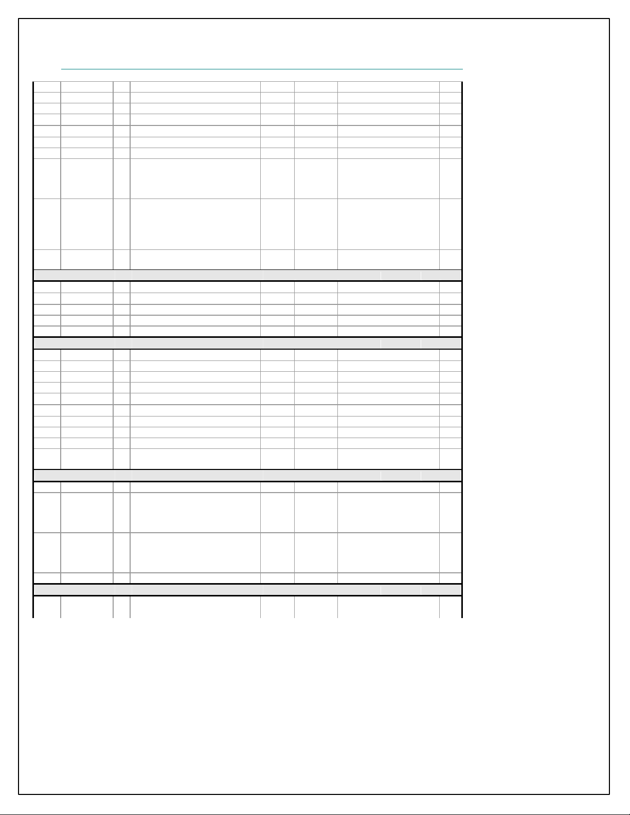
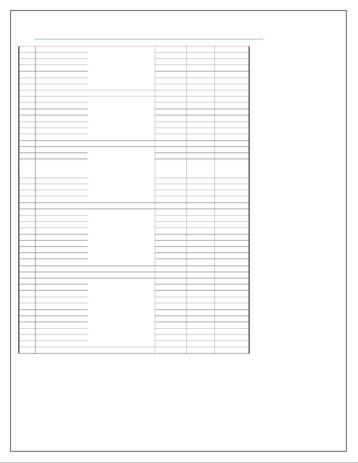
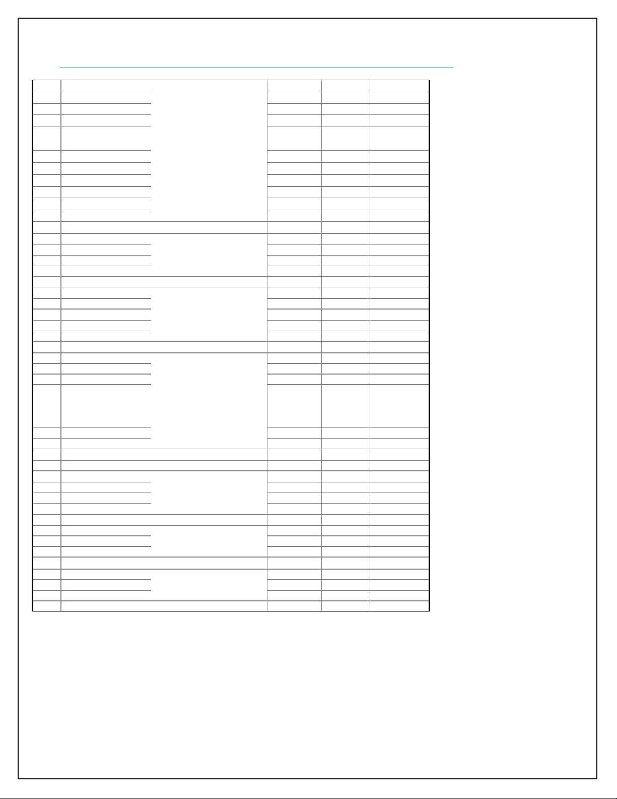
2.2 Pin Description
Ball
Name Dir Description
13X13
JTAG Port
E4 JTRST# I JTAG test port reset input PD Input
E3 JTCK I JTAG test port clock input PU Input
E2 JTDI I JTAG test port data input PU Input
E1 JTMS I JTAG test port mode swit ch PU Input
F5 JTDO O JTAG test port data output 0
F4 JRTCK O JTAG test port returned clock output 0
RF Parallel Control Unit
F3 BPI_BUS0 O RF hard-wire control bus 0 0
F2 BPI_BUS1 O RF hard-wire control bus 1 0
G5 BPI_BUS2 O RF hard- wire control bus 2 0
G4 BPI_BUS3 O RF hard- wire control bus 3 0
G3 BPI_BUS4 IO RF hard-wire control bus 4 Input
G2 BPI_BUS5 IO RF hard-wire control bus 5 Input
G1 BPI_BUS6 IO RF hard-wire control bus 6 GPIO10 BPI_BUS6 PD Input
H5 BPI_BUS7 IO RF hard-wire control bus 7 GPIO11 BPI_BUS7 PD Input
H4 BPI_BUS8 IO RF hard-wire control bus 4 GPIO12 BPI_BUS8 13MHz 32KHz PD Input
H3 BPI_BUS9 IO RF hard-wire control bus 5 GPIO13 BPI_BUS9 BSI_CS1 PD Input
RF Serial Control Unit
H1 BSI_CS0 O RF 3-wire interface chip select 0 0
J5 BSI_DATA O RF 3-wire interface data output 0
J4 BSI_CLK O RF 3-wire interface clock output 0
PWM Interface
R3 PWM1 IO Pulse width modulated signal 1 GPIO21 PWM1 DSP_GPO0 TBTXFS PD Input
R2 PWM2 IO Pulse width modulated signal 2 GPIO22 PWM2 DSP_GPO1 TBRXEN PD Input
T4 ALERTER IO Pulse width modulated signal for buzzer GPIO23 ALERTER DSP_GPO2 BTRXFS PD Input
Serial LCD/PM IC Interface
J3 LSCK IO Serial display interface data output GPIO16 LSCK TDMA_CK TBTXEN PD Input
J2 LSA0 IO Serial display interface address output GPIO17 LSA0 TDMA_D1 TDTIRQ PD Input
J1 LSDA IO Serial display interface clock output GPIO18 LSDA TDMA_D0 TCTIRQ2 PD Input
K4 LSCE0# IO Serial display interface chip select 0
output
K3 LSCE1# IO Serial display interface chip select 1
output
Parallel LCD/Nand-Flash Interface
K2 LPCE1# IO Parallel display interface chip select 1
output
L5 LPCE0# O Parallel display interface chip select 0
output
L4 LRST# O Parallel display interface Reset Signal 1
L3 LRD# O Parallel display interface Read Strobe 1
L2 LPA0 O Parallel display interface address output 1
L1 LWR# O Parallel display interface Write Strobe 1
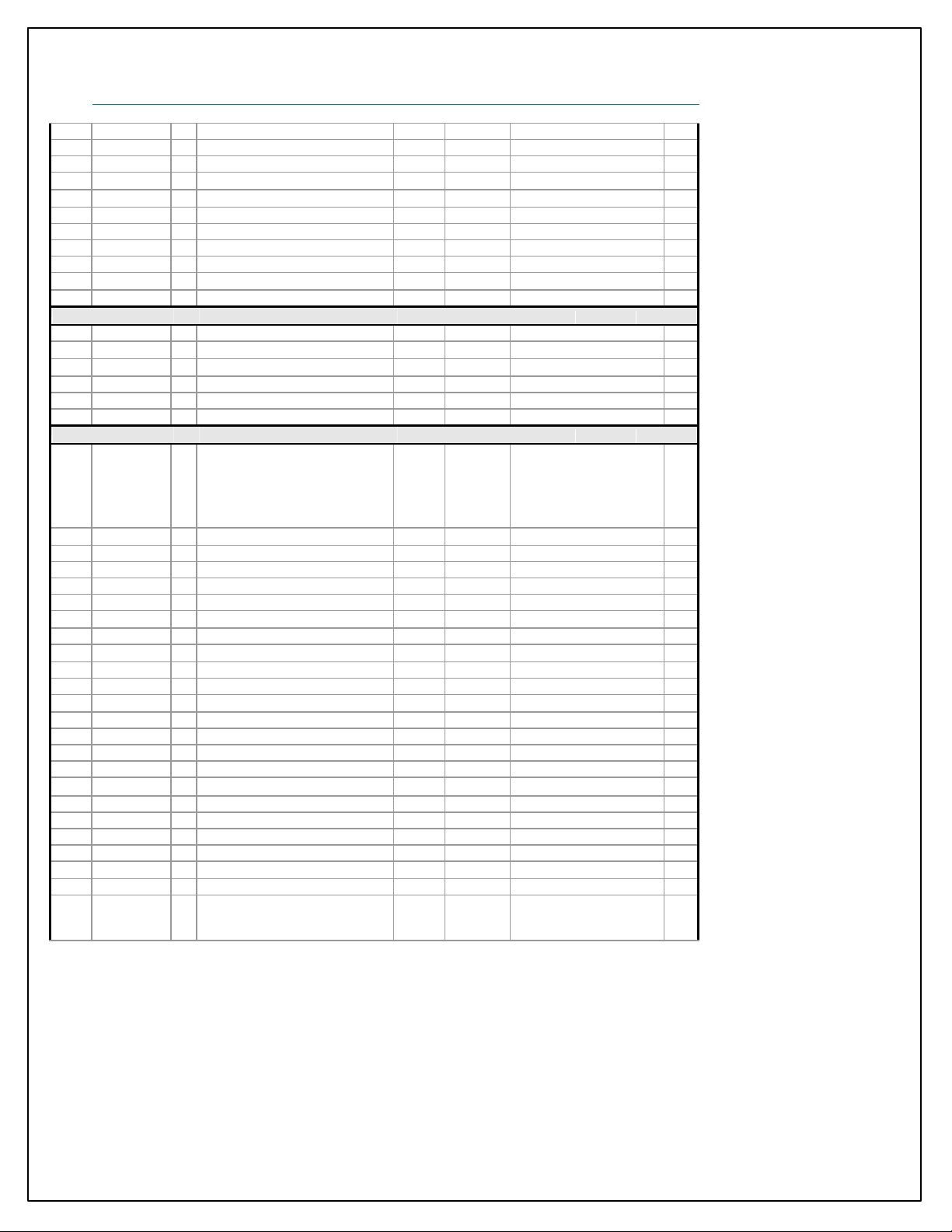
M5 NLD7 IO Parallel LCD/Nand-Flash Data 7 PD Input
Mode0 Mode1 Mode2 Mode3
GPIO19 LSCE0# TDMA_FS TCTIRQ1 PU Input
GPIO20 LSCE1# LPCE2# TEVTVAL PU Input
GPIO24 LPCE1# DSP_TID0 MCU_TD0 PU Input
PU Input
PU/
PD
Rese
t
19/418 MediaTek Inc. Confidential
MT6219 GSM/GPRS Baseband Processor Data Sheet Revision 1.01
M4 NLD6 IO Parallel LCD/Nand-Flash Data 6 PD Input
M3 NLD5 IO Parallel LCD/Nand-Flash Data 5 PD Input
N5 NLD4 IO Parallel LCD/Nand-Flash Data 4 PD Input
N4 NLD3 IO Parallel LCD/Nand-Flash Data 3 PD Input
N3 NLD2 IO Parallel LCD/Nand-Flash Data 2 PD Input
N2 NLD1 IO Parallel LCD/Nand-Flash Data 1 PD Input
N1 NLD0 IO Parallel LCD/Nand-Flash Data 0 PD Input
P5 NRNB IO Nand-Flash Read/Busy Flag GPIO25 NRNB DSP_TID1 MCU_TID1 PU Input
P4 NCLE IO Nand-Flash Command Latch Signal GPIO26 NCLE DSP_TID2 MCU_TID2 PD Input
P3 NALE IO Nand-Flash Address Latch Signal GPIO27 NALE DSP_TID3 MCU_TID3 PD Input
P2 NWE# IO Nand-Flash Write Strobe GPIO28 NWE# DSP_TID4 MCU_DID PU Input
P1 NRE# IO Nand-Flash Read Strobe GPIO29 NRE# DSP_TID5 MCU_DFS PU Input
R4 NCE# IO Nand-Flash Chip select output GPIO30 NCE# DSP_TID6 MCU_DCK PU Input
SIM Card Interface
L18 SIMRST O SIM card reset output 0
L17 SIMCLK O SIM card clock output 0
K15 SIMVCC O SIM card supply power control 0
K16 SIMSEL O SIM card supply power select GPIO32 SIMSEL PD Input
K17 SIMDATA IO SIM card data input/output 0
Dedicated GPIO Interface
U2 GPIO0 IO General purpose input/output 0 GPIO0 DSP_GPO3 PD Input
M19 GPIO1 IO General purpose input/output 1 GPIO1 DICK PD Input
L15 GPIO2 IO General purpose input/output 2 GPIO2 DID PD Input
L16 GPIO3 IO General purpose input/output 3 GPIO3 DIMS PD Input
C17 GPIO4 IO General purpose input/output 4 GPIO4 DSP_CLK DSPLCK TRASD4 PD Input
A19 GPIO5 IO General purpose input/output 5 GPIO5 AHB_CLK DSPLD3 TRASD3 PD Input
B18 GPIO6 IO General purpose input/output 6 GPIO6 ARM_CLK DSPLD2 TRASD2 PD Input
B17 GPIO7 IO General purpose input/output 7 GPIO7 SLOW_CK DSPLD1 TRASD1 PD Input
A18 GPIO8 IO General purpose input/output 19 GPIO8 SCL DSPLD0 TRASD0 PD Input
A17 GPIO9 IO General purpose input/output 21 GPIO9 SDA DSPLSYNC TRARSY
NC
Miscellaneous
U1 SYSRST# I System reset input active low Input
R18 WATCHDOG# O Watchdog reset output 1
PD Input
T3 SRCLKENAN O External TCXO enable output active
low
T1 SRCLKENA O External TCXO enable output active
high
T2 SRCLKENAI IO External TCXO enable input GPIO31 SRCLKEN
E5 IBOOT I Boot Device Configuration Input PD Input
Keypad Interface
G17 KCOL6 I Keypad column 6 PU Input
G18 KCOL5 I Keypad column 5 PU Input
20/418 MediaTek Inc. Confidential
GPO1 SRCLKEN
AN
GPO0 SRCLKENA 1
AI
0
PD Input
MT6219 GSM/GPRS Baseband Processor Data Sheet Revision 1.01
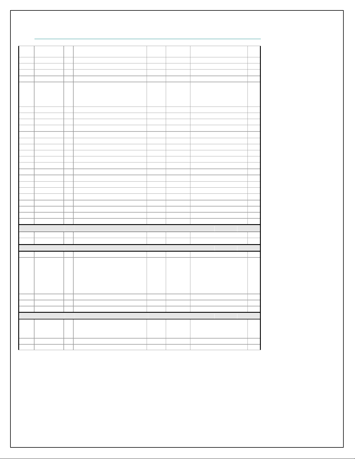
G19 KCOL4 I Keypad column 4 PU Input
F15 KCOL3 I Keypad column 3 PU Input
F16 KCOL2 I Keypad column 2 PU Input
F17 KCOL1 I Keypad column 1 PU Input
F18 KCOL0 I Keypad column 0 PU Input
F19 KROW5 O Keypad row 5 0
E16 KROW4 O Keypad row 4 0
E17 KROW3 O Keypad row 3 0
E18 KROW2 O Keypad row 2 0
D16 KROW1 O Keypad row 1 0
D19 KROW0 O Keypad row 0 0
External Interrupt Interface
V1 EINT0 I External interrupt 0 PU Input
U3 EINT1 I External interrupt 1 PU Input
W1 EINT2 I External interrupt 2 PU Input
V2 EINT3 I External interrupt 3 PU Input
R5 MIRQ I Interrupt to MCU GPIO41 MIRQ 13MHz 32KHz PU Input
R17 MFIQ I Interrupt to MCU GPIO42 MFIQ PU Input
External Memory Interface
R16 ED0 IO External memory data bus 0 Input
R15 ED1 IO External memory data bus 1 Input
T19 ED2 IO External memory data bus 2 Input
T17 ED3 IO Ext ernal memory data bus 3 Input
U19 ED4 IO External memory data bus 4 Input
U18 ED5 IO External memory data bus 5 Input
V18 ED6 IO External memory data bus 6 Input
W19 ED7 IO External memory data bus 7 Input
U17 ED8 IO External memory data bus 8 Input
V17 ED9 IO External memory data bus 9 Input
W17 ED10 IO External memory data bus 10 Input
T16 ED11 IO External memory data bus 11 Input
W16 ED12 IO External memory data bus 12 Input
T15 ED13 IO External memory data bus 13 Input
U15 ED14 IO External memory data bus 14 Input
V15 ED15 IO External memory data bus 15 Input
U14 ERD# O External memory read strobe 1
W14 EWR# O External memory write strobe 1
R13 ECS0# O External memory chip select 0 1
T13 ECS1# O External memory chip select 1 1
U13 ECS2# O External memory chip select 2 1
V13 ECS3# O External memory chip select 3 1
R12 ECS4# O External memory chip select 4 GPIO54 ECS4# PU 1
T12 ECS5# O External memory chip select 5 GPIO53 ECS5# PU 1
U12 ECS6# O External memory chip select 6 GPIO52 ECS6# PU 1
W12 ECS7# O External memory chip select 7 GPIO40 ECS7# PU 1
R14 ELB# O External memory lower byte strobe 1
T14 EUB# O External memory upper byte strobe 1
T11 EPDN# O Power Down Control Signal for
PSRAM
21/418 MediaTek Inc. Confidential
GPO2 EPDN# 0
MT6219 GSM/GPRS Baseband Processor Data Sheet Revision 1.01
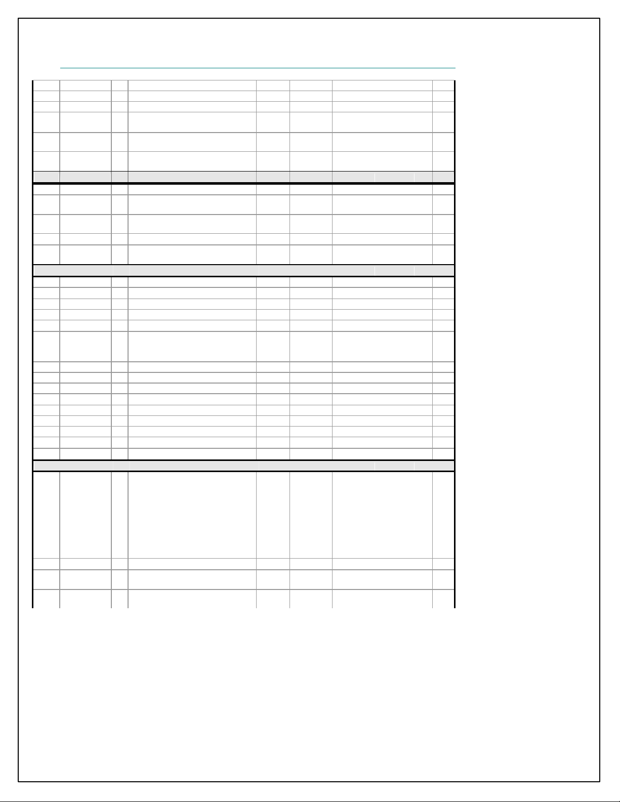
U11 EADV# O Address valid for burst mode flash
memory
V11 ECLK O Clock for flash memory 0
R10 EA0 O External memory address bus 0 0
T10 EA1 O External memory address bus 1 0
U10 EA2 O External memory address bus 2 0
W10 EA3 O External memory address bus 3 0
T9 EA4 O External memory address bus 4 0
U9 EA5 O External memory address bus 5 0
V9 EA6 O External memory address bus 6 0
R8 EA7 O External memory address bus 7 0
T8 EA8 O External memory address bus 8 0
W8 EA9 O External memory address bus 9 0
R7 EA10 O External memory address bus 10 0
T7 EA11 O External memory address bus 11 0
U7 EA12 O External memory address bus 12 0
V7 EA13 O External memory address bus 13 0
R6 EA14 O External memory address bus 14 0
T6 EA15 O External memory address bus 15 0
U6 EA16 O External memory address bus 16 0
W6 EA17 O External memory address bus 17 0
T5 EA18 O External memory address bus 18 0
U5 EA19 O External memory address bus 19 0
V5 EA20 O External memory address bus 20 0
W5 EA21 O External memory address bus 21 0
V4 EA22 O External memory address bus 22 0
U4 EA23 O External memory address bus 23 0
W3 EA24 O External memory address bus 24 GPO3 EA24 0
W2 EA25 O External memory address bus 25 GPO4 EA25 13MHz 32KHz 0
USB Interface
P16 USB_DP IO USB D+ Input/Output
P17 USB_DM IO USB D- Input/Output
Memory Card Interface
P19 MCCM0 IO SD Command/MS Bus State Output
N15 MCDA0 IO SD Serial Data IO 0/MS Serial Data IO
N16 MCDA1 IO SD Serial Data IO 1
N17 MCDA2 IO SD Serial Data IO 2
N18 MCDA3 IO SD Serial Data IO 3
N19 MCCK O SD Serial Clock/MS Serial Clock
Output
M16 MCPWRON O SD Power On Control Output
M17 MCWP I SD Write Protect Input GPIO15 MCWP PU
M18 MCINS I SD Card Detect Input GPIO14 MCINS PU
UART Interface
K18 URXD1 I UART 1 receive data PU Input
K19 UTXD1 O UART 1 transmit data 1
J16 UCTS1 I UART 1 clear to send PU Input
J17 URTS1 O UART 1 request to send 1
J18 URXD2 IO UART 2 receive data GPIO35 URXD2 UCTS3 PU Input
22/418 MediaTek Inc. Confidential
1
MT6219 GSM/GPRS Baseband Processor Data Sheet Revision 1.01
J19 UTXD2 IO UART 2 transmit data GPIO36 UTXD2 URTS3 PU Input
H15 URXD3 IO UART 3 receive data GPIO33 URXD3 PU Input
H16 UTXD3 IO UART 3 transmit data GPIO34 UTXD3 PU Input
H17 IRDA_RXD IO IrDA receive data GPIO37 IRDA_RXD UCTS2 PU Input
G15 IRDA_TXD IO IrDA transmit data GPIO38 IRDA_TXD URTS2 PU Input
G16 IRDA_PDN IO IrDA Power Down Control GPIO39 IRDA_PDN PU Input
Digital Audio Interface
D17 DAICLK IO DAI clock output GPIO43 DAICLK DSPLD7 TRACLK PU Input
D18 DAIPCMOUT IO DAI pcm data out GPIO44 DAIPCMO
C19 DAIPCMIN IO DAI pcm data input GPIO45 DAIPCMIN DSPLD5 TRASD7 PU Input
C18 DAIRST IO DAI reset signal input GPIO47 DAIRST DSPLD4 TRASD6 PU Input
B19 DAISYNC IO DAI frame synchronization signal
CMOS Sensor Interface
J12 CMRST IO CMOS sensor reset signal output GPIO48 CMRST Z Input
K12 CMPDN IO CMOS sensor power down control GPIO49 CMPDN Z Input
H12 CMVREF I Sensor vertical refe rence signal input Input
H11 CMHREF I Sensor horizontal reference signal input Input
H9 CMPCLK I CMOS sensor pixel clock input Input
H10 CMMCLK O CMOS sensor master clock output Outp
H8 CMDAT9 I CMOS sensor data input 9 Input
J8 CMDAT8 I CMOS sensor data input 8 Input
K8 CMDAT7 I CMOS sensor data input 7 Input
L8 CMDAT6 I CMOS sensor data input 6 Input
M8 CMDAT5 I CMOS sensor data input 5 Input
M9 CMDAT4 I CMOS sensor data input 4 Input
M10 CMDAT 3 I CMOS sensor data input 3 Input
M11 CMDAT2 I CMOS sensor data input 2 Input
M12 CMDAT1 IO CMOS sensor data input 1 GPIO50 CMDAT1 PD Input
L12 CMDAT0 IO CMOS sensor data input 0 GPIO51 CMDAT2 PD Input
Analog Interface
B15 AU_MOUL Audio analog output left channel
A15 AU_MOUR Audio analog output right channel
C14 AU_M_BYP Audio DAC bypass pin
B14 AU_FMINL FM radio analog input left channel
A14 AU_FMINR FM radio analog input right channel
D13 AU_OUT1_P Earphone 1 amplifier output (+)
C13 AU_OUT1_N Earphone 1 amplifier output (-)
B12 AU_OUT0_N Earphone 0 amplifier output (-)
A12 AU_OUT0_P Earphone 0 amplifier output (+)
C12 AU_MICBIA
S_P
D12 AU_MICBIA
S_N
output
Microphone bias supply (+)
Microphone bias supply (-)
GPIO46 DAISYNC BFEPRBO TRASD5 PU Input
UT
DSPLD6 TRASYNC PD Input
ut
23/418 MediaTek Inc. Confidential
MT6219 GSM/GPRS Baseband Processor Data Sheet Revision 1.01
C11 AU_VREF_N Audio reference voltage (-)
B11 AU_VREF_P Audio reference voltage (+)
D10 AU_VIN0_P Microphone 0 amplifier input (+)
C10 AU_VIN0_N Microphone 0 amplifier input (-)
B10 AU_VIN1_N Microphone 1 amplifier input (-)
A10 AU_VIN1_P Microphone 1 amplifier input (+)
D9 BDLAQP Quadrature input (Q+) baseband codec
downlink
C9 BDLAQN Quadrature input (Q-) baseband codec
downlink
A9 BDLAIN In-phase input (I+) baseband codec
downlink
B9 BDLAIP In-phase input (I-) baseband codec
downlink
B8 BUPAIP In-phase output (I+) baseband codec
uplink
A8 BUPAIN In-phase output (I-) baseband codec
uplink
C8 BUPAQN Quadrature output (Q+) baseband codec
uplink
D8 BUPAQP Quadrature output (Q-) baseband codec
uplink
B7 APC Automatic power control DAC output
D6 AUXADIN0 Auxiliary ADC input 0
C6 AUXADIN1 Auxiliary ADC input 1
B6 AUXADIN2 Auxiliary ADC input 2
A6 AUXADIN3 Auxiliary ADC input 3
C5 AUXADIN4 Auxiliary ADC input 4
B5 AUXADIN5 Auxiliary ADC input 5
A5 AUXADIN6 Auxiliary ADC input 6
C4 AUX_REF Auxiliary ADC reference voltage input
B4 AFC Automatic frequency control DAC
output
A4 AFC_BYP Automatic frequency control DAC
bypass capacitance
VCXO Interface
A2 SYSCLK 13MHz or 26MHz system clock input
RTC Interface
C2 XIN 32.768 KHz crystal input
B1 XOUT 32.768 KHz crystal output
C1 BBWAKEUP O Baseband power on/off control 1
Supply Voltages
D1 VDDK Supply voltage of internal logic
M1 VDDK Supply voltage of internal logic
V8 VDDK Supply voltage of internal logic
V16 VDDK Supply voltage of internal logic
H19 VDDK Supply voltage of internal logic
C16 VDDK Supply voltage of internal logic
W4 VDD33_EMI Supply voltage of memory interface
driver
24/418 MediaTek Inc. Confidential
MT6219 GSM/GPRS Baseband Processor Data Sheet Revision 1.01
W7 VDD33_EMI Supply voltage of memory interface
driver
W9 VDD33_EMI Supply voltage of memory interface
driver
W11 VDD33_EMI Supply voltage of memory interface
driver
W13 VDD33_EMI Supply voltage of memory interface
driver
W15 VDD33_EMI Supply voltage of memory interface
driver
W18 VDD33_EMI Supply voltage of memory interface
driver
T18 VDD33_EMI Supply voltage of memory interface
driver
V3 VSS33_EMI Ground of memory interface driver
V6 VSS33_EMI Ground of memory interface driver
U8 VSS33_EMI Ground of memory interface driver
V10 VSS33_EMI Ground of memory interface driver
V12 VSS33_EMI Ground of memory interface driver
V14 VSS33_EMI Ground of memory interface driver
U16 VSS33_EMI Ground of memory interface driver
V19 VSS33_EMI Ground of memory interface driver
R19 VSS33_EMI Ground of memory interface driver
P15 VDD33_USB Supply voltage of drivers for USB
D4 VDD33 Supply voltage of drivers exce pt
memory interface and USB
F1 VDD33 Supply voltage of drivers except
memory interface and USB
K1 VDD33 Supply voltage of drivers except
memory interface and USB
R1 VDD33 Supply voltage of drivers except
memory interface and USB
L19 VDD33 Supply voltage of drivers except
memory interface and USB
E19 VDD33 Supply voltage of drivers except
memory interface and USB
E15 VDD33 Supply voltage of drivers except
memory interface and USB
E13 VDD33 Supply voltage of drivers except
memory interface and USB
E11 VDD33 Supply voltage of drivers except
memory interface and USB
E6 VDD33 Supply voltage of drivers except
memory interface and USB
A3 VSS33 Ground of drivers except memory
interface
D2 VSS33 Ground of drivers except memory
interface
D5 VSS33 Ground of drivers except memory
interface
H2 VSS33 Ground of drivers except memory
interface
25/418 MediaTek Inc. Confidential
MT6219 GSM/GPRS Baseband Processor Data Sheet Revision 1.01
M2 VSS33 Ground of drivers except memory
P18 VSS33 Ground of drivers except memory
H18 VSS33 Ground of drivers except memory
A16 VSS33 Ground of drivers except memory
B16 VSS33 Ground of drivers except memory
E14 VSS33 Ground of drivers except memory
E12 VSS33 Ground of drivers except memory
E7 VSS33 Ground of drivers except memory
B3 AVDD_PLL Supply voltage for PLL
C3 AVSS_PLL Ground for PLL supply
B2 AVDD_RTC Supply voltage for Real Time Clock
Analog Supplies
C15 AVDD_MBUF Supply Voltage for Audio band section
D14 AVSS_MBUF GND for Audio band section
B13 AVDD_BUF Supply voltage for voice band transmit
A13 AVSS_BUF GND for voice band transmit section
D11 AVDD_AFE Supply voltage for voice band receive
A11 AGND_AFE GND reference voltage for voice band
E10 AVSS_AFE GND for voice band receive section
E9 AGND_RFE GND reference voltage for baseband
E8 AVSS_GSMR
FTX
D7 AVDD_GSM
RFTX
C7 AVSS_RFE GND for baseband receive section,
A7 AVDD_RFE Supply voltage for baseband receive
interface
interface
interface
interface
interface
interface
interface
interface
section
section
section
section, APC, AFC and AUXADC
GND for baseband transmit section
Supply voltage for baseband transmit
section
APC, AFC and AUXADC
section, APC, AFC and AUXADC
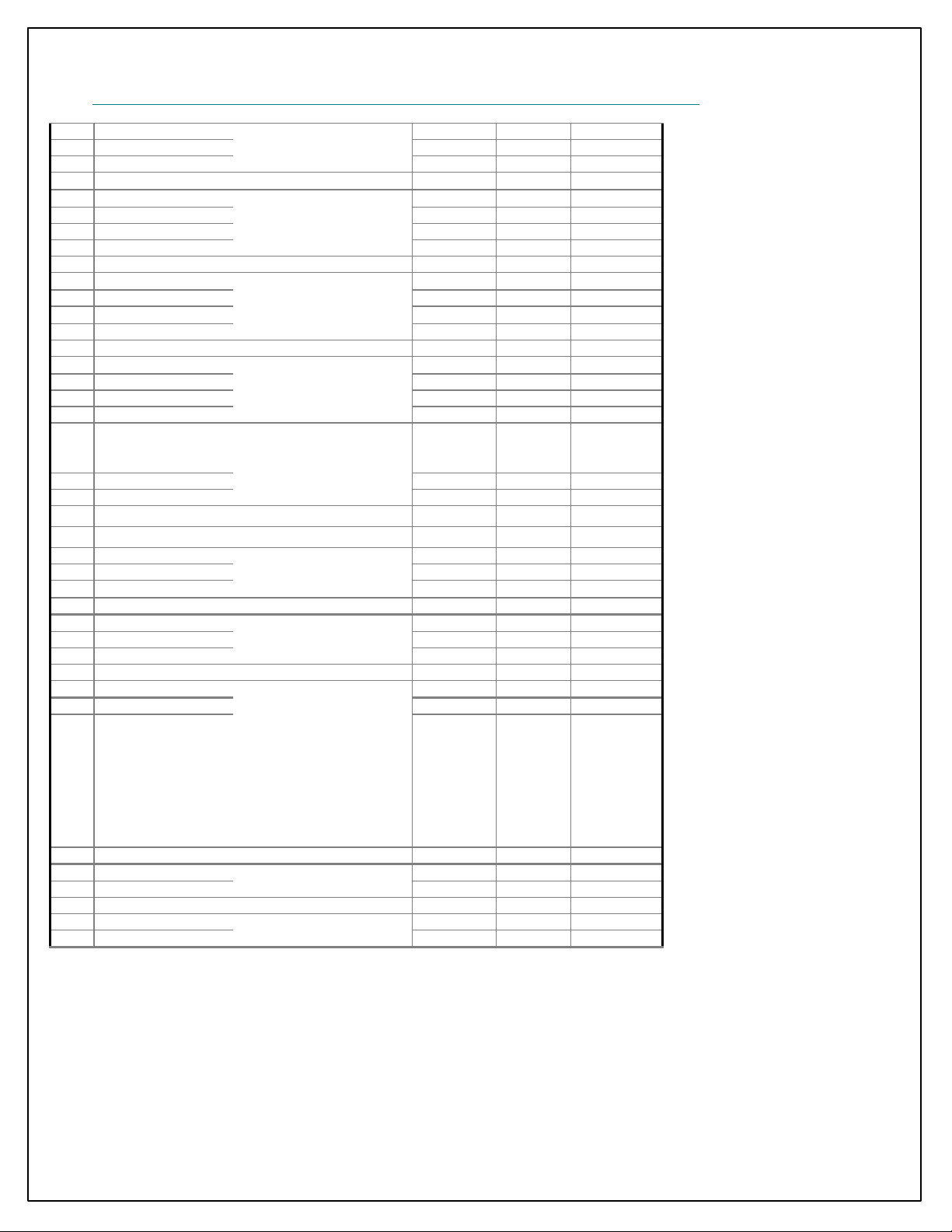
Table 2 Pin Descriptions (Bolded types are functions at reset)
26/418 MediaTek Inc. Confidential
MT6219 GSM/GPRS Baseband Processor Data Sheet Revision 1.01
2.3 Power Description
Ball
Name IO Supply IO GND Core Supply Core GND Remark
13X13
B17 GPIO7 VDDK VSSK
A18 GPIO8 VDDK VSSK
A17 GPIO9
B16 VSS33
A16 VSS33
C16 VDDK Typ. 1.2V
E15 VDD33 Typ. 2.8V
E14 VSS33
E13 VDD33 Typ. 2.8V
E12 VSS33
E11 VDD33 Typ. 2.8V
E7 VSS33
E6 VDD33 Typ. 2.8V
D5 VSS33
J12 CMRST VDDK VSSK
K12 CMPDN VDDK VSSK
H12 CMVREF VDDK VSSK
H11 CMHREF VDDK VSSK
H9 CMPCLK VDDK VSSK
H10 CMMCLK
D4 VDD33 Typ. 2.8V
H8 CMDAT9 VDDK VSSK
J8 CMDAT8 VDDK VSSK
K8 CMDAT7 VDDK VSSK
L8 CMDAT6 VDDK VSSK
M8 CMDAT5 VDDK VSSK
M9 CMDAT4 VDDK VSSK
M10 CMDAT3 VDDK VSSK
M11 CMDAT2 VDDK VSSK
M12 CMDAT1 VDDK VSSK
L12 CMDAT0
A3 VSS33
B3 AVDD_PLL Typ. 2.8V
A2 SYSCLK AVDD_PLL AVSS_PLL AVDD_PLL AVSS_PLL
C3 AVSS_PLL
B2 AVDD_RTC Typ. 1. 2V
B1 XOUT AVDD_RTC VSS33 AVDD_RTC VSS33
C2 XIN AVDD_RTC VSS33 AVDD_RTC VSS33
C1 BBWAKEUP AVDD_RTC VSS33 AVDD_RTC VSS33
D2 VSS33
D3 TESTMODE VDD33 VSS33 VDDK VSSK
D1 VDDK Typ. 1.2V
E5 IBOOT VDDK VSSK
E4 JTRST#
VDD33 VSS33
VDDK VSSK
VDD33 VSS33
VDDK VSSK
VDD33 VSS33
VDDK VSSK
VDD33 VSS33
VDDK VSSK
27/418 MediaTek Inc. Confidential
MT6219 GSM/GPRS Baseband Processor Data Sheet Revision 1.01
E3 JTCK VDDK VSSK
E2 JTDI VDDK VSSK
E1 JTMS VDDK VSSK
F5 JTDO VDDK VSSK
F4 JRTCK VDDK VSSK
F3 BPI_BUS0 VDDK VSSK
F2 BPI_BUS1 VDDK VSSK
F1 VDD33 Typ. 2.8V
G5 BPI_BUS2 VDDK VSSK
G4 BPI_BUS3 VDDK VSSK
G3 BPI_BUS4 VDDK VSSK
G2 BPI_BUS5 VDDK VSSK
G1 BPI_BUS6 VDDK VSSK
H5 BPI_BUS7 VDDK VSSK
H4 BPI_BUS8
H2 VSS33
H3 BPI_BUS9 VDDK VSSK
H1 BSI_CS0 VDDK VSSK
J5 BSI_DATA VDDK VSSK
J4 BSI_CLK VDDK VSSK
J3 LSCK VDDK VSSK
J2 LSA0 VDDK VSSK
J1 LSDA VDDK VSSK
K4 LSCE0# VDDK VSSK
K3 LSCE1#
K1 VDD33 Typ. 2.8V
K2 LPCE1# VDDK VSSK
L5 LPCE0# VDDK VSSK
L4 LRST# VDDK VSSK
L3 LRD# VDDK VSSK
L2 LPA0 VDDK VSSK
L1 LWR# VDDK VSSK
M5 NLD7 VDDK VSSK
M4 NLD6 VDDK VSSK
M3 NLD5
M2 VSS33
M1 VDDK Typ. 1.2V
N5 NLD4 VDDK VSSK
N4 NLD3 VDDK VSSK
N3 NLD2 VDDK VSSK
N2 NLD1 VDDK VSSK
N1 NLD0 VDDK VSSK
P5 NRNB VDDK VSSK
P4 NCLE VDDK VSSK
P3 NALE VDDK VSSK
P2 NEW# VDDK VSSK
P1 NRE# VDDK VSSK
R4 NCE#
R1 VDD33 Typ. 2.8V
28/418 MediaTek Inc. Confidential
VDD33 VSS33
VDDK VSSK
VDD33 VSS33
VDDK VSSK
VDD33 VSS33
VDDK VSSK
VDD33 VSS33
VDDK VSSK
MT6219 GSM/GPRS Baseband Processor Data Sheet Revision 1.01
R3 PWM1 VDDK VSSK
R2 PWM2 VDDK VSSK
T4 ALERTER VDDK VSSK
T1 SRCLKENA VDDK VSSK
T3 SRCLKENAN VDDK VSSK
T2 SRCLKENAI VDDK VSSK
U1 SYSRST# VDDK VSSK
U2 GPIO0 VDDK VSSK
V1 EINT0 VDDK VSSK
U3 EINT1 VDDK VSSK
W1 EINT2 VDDK VSSK
V2 EINT3
V3 VSS33_EMI
W2 EA25 VDDK VSSK
W3 EA24 VDDK VSSK
U4 EA23 VDDK VSSK
V4 EA22
W4 VDD33_EMI Typ. 1.8~2.8V
R5 MIRQ VDDK VSSK
W5 EA21 VDDK VSSK
V5 EA20 VDDK VSSK
U5 EA19 VDDK VSSK
T6 EA18
V6 VSS33_EMI
W6 EA17 VDDK VSSK
U6 EA16 VDDK VSSK
T6 EA15 VDDK VSSK
R6 EA14
W7 VDD33_EMI Typ. 1.8~2.8V
V7 EA13 VDDK VSSK
U7 EA12 VDDK VSSK
T7 EA11 VDDK VSSK
R7 EA10
V8 VDDK Typ. 1.2V
U8 VSS33_EMI
W8 EA9 VDDK VSSK
T8 EA8 VDDK VSSK
R8 EA7 VDDK VSSK
V9 EA6
W9 VDD33_EMI Typ. 1.8~2.8V
U9 EA5 VDDK VSSK
T9 EA4 VDDK VSSK
W10 EA3
V10 VSS33_EMI
U10 EA2 VDDK VSSK
T10 EA1 VDDK VSSK
R10 EA0
W11 VDD33_EMI Typ. 1.8~2.8V
29/418 MediaTek Inc. Confidential
VDD33 VSS33
VDDK VSSK
VDD33_EMI VSS33_EMI
VDDK VSSK
VDD33_EMI VSS33_EMI
VDDK VSSK
VDD33_EMI VSS33_EMI
VDDK VSSK
VDD33_EMI VSS33_EMI
VDDK VSSK
VDD33_EMI VSS33_EMI
VDDK VSSK
VDD33_EMI VSS33_EMI
VDDK VSSK
VDD33_EMI VSS33_EMI
VDDK VSSK
MT6219 GSM/GPRS Baseband Processor Data Sheet Revision 1.01
U11 EADV# VDDK VSSK
V11 ECLK VDDK VSSK
T11 EPDN#
V12 VSS33_EMI
W12 ECS7# VDDK VSSK
U12 ECS6# VDDK VSSK
T12 ECS5# VDDK VSSK
R12 ECS4#
W13 VDD33_EMI Typ. 1.8~2.8V
V13 ECS3# VDDK VSSK
U13 ECS2# VDDK VSSK
T13 ECS1# VDDK VSSK
R13 ECS0#
V14 VSS33_EMI
W14 EWR# VDDK VSSK
U14 ERD# VDDK VSSK
T14 EUB# VDDK VSSK
R14 ELB#
W15 VDD33_EMI Typ. 1.8~2.8V
V15 ED15 VDDK VSSK
U15 ED14 VDDK VSSK
T15 ED13 VDDK VSSK
W16 ED12
V16 VDDK 1.2V
U16 VSS33_EMI
T16 ED11 VDDK VSSK
W17 ED10 VDDK VSSK
V17 ED9
W18 VDD33_EMI Typ. 1.8~2.8V
U17 ED8 VDDK VSSK
W19 ED7 VDDK VSSK
V18 ED6
V19 VSS33_EMI
U18 ED5 VDDK VSSK
U19 ED4 VDDK VSSK
T17 ED3
T18 VDD33_EMI Typ. 1.8~2.8V
T19 ED2 VDDK VSSK
R15 ED1 VDDK VSSK
R16 ED0 VDDK VSSK
R17 MFIQ VDDK VSSK
R18 WATCHDOG
R19 VSS33_EMI
P15 VDD33_USB Typ. 3.3V
P16 USB_DP VDDK VSSK
P17 USB_DM
P18 VSS33
P19 MCCM0 VDDK VSSK
N15 MCDA0
30/418 MediaTek Inc. Confidential
VDD33_EMI VSS33_EMI
VDD33_EMI VSS33_EMI
VDD33_EMI VSS33_EMI
VDD33_EMI VSS33_EMI
VDD33_EMI VSS33_EMI
VDD33_EMI VSS33_EMI
VDD33_EMI VSS33_EMI
VDD33_EMI VSS33_EMI
VDD33_EMI VSS33_EMI
VDD33_USB VSS33
VDD33
VSS33
VDDK VSSK
VDDK VSSK
VDDK VSSK
VDDK VSSK
VDDK VSSK
VDDK VSSK
VDDK VSSK
VDDK VSSK
VDDK VSSK
VDDK VSSK
VDDK VSSK
 Loading...