

MediaTek MT6217 Schematics

MT6217 GSM/GPRS
Baseband Processor Data Sheet
Revision 1.01
Apr. 18, 2005

MT6217 GSM/GPRS Baseband Processor Data Sheet Revision 1.01
Revision History
Revision Date Comments
1.00 Sep. 01, 2004 First Release
1.01 Apr. 18, 2005 1) Corrected interrupt source naming in MCU Subsystem > Interrupt Controller > Table 12.
GPI-FIQ -> MFIQ, GPI -> MIRQ
2) Corrected GPIO_MODE6 register description from nIRQ -> MIRQ and nFIQ -> MFIQ
3) Corrected LCD_SDAT0 and LCD_SDAT1 register address
4) Updated EMI_GEN register
5) Updated GPIO16, GPIO17, GPIO18 PU/PD control, and added GPIO40 in product
description
6) Updated GPIO_MODE2 register
7) Added NLD15~NLD8 digital pin characteristics
8) Updated driving strength in digital pin characteristics
2/349 MediaTek Inc. Confidential

MT6217 GSM/GPRS Baseband Processor Data Sheet Revision 1.01
TABLE OF CONTENTS
Revision History ......................................................................................................................................2
1. System Overview...............................................................................................................................2
1.1 Features...........................................................................................................................................................................................2
1.2 General Description ......................................................................................................................................................................2
2 Product Description..........................................................................................................................2
2.1 Pin Outs ...........................................................................................................................................................................................2
2.2 Pin Description ..............................................................................................................................................................................2
2.3 Power Description .........................................................................................................................................................................2
3 Micro-Controller Unit Subsystem...................................................................................................2
3.1 Processor Core ...............................................................................................................................................................................2
3.2 Memory Management ..................................................................................................................................................................2
3.3 Bus System.....................................................................................................................................................................................2
3.4 Direct Memory Access.................................................................................................................................................................2
3.5 Interrupt Controller.......................................................................................................................................................................2
3.6 Internal Memory Controller ........................................................................................................................................................2
3.7 External Memory Interface ..........................................................................................................................................................2
4 Microcontroller Peripherals ............................................................................................................2
4.1 Pulse-Width Modulation Outputs ...............................................................................................................................................2
4.2 Alerter.............................................................................................................................................................................................2
4.3 SIM Interface .................................................................................................................................................................................2
4.4 Keypad Scanner.............................................................................................................................................................................2
4.5 General Purpose Inputs/Outputs .................................................................................................................................................2
4.6 General Purpose Timer.................................................................................................................................................................2
4.7 UART..............................................................................................................................................................................................2
4.8 IrDA Framer ...................................................................................................................................................................................2
4.9 Real Time Clock............................................................................................................................................................................2
4.10 Auxiliary ADC Unit ...................................................................................................................................................................... 2
5 Microcontroller Coprocessors .........................................................................................................2
5.1 GPRS Cipher Unit .........................................................................................................................................................................2
5.2 Divider............................................................................................................................................................................................2
5.3 CSD Accelerator ............................................................................................................................................................................2
5.4 FCS Codec......................................................................................................................................................................................2
6 Multi-Media Subsystem...................................................................................................................2
6.1 LCD Interface ................................................................................................................................................................................2
6.2 JPEG Decoder................................................................................................................................................................................2
6.3 Image Resizer................................................................................................................................................................................2
6.4 NAND FLASH interface .............................................................................................................................................................2
6.5 USB Device Controller ................................................................................................................................................................ 2
6.6 Memory Stick and SD Memory Card Controller .....................................................................................................................2
7 Audio Front-end................................................................................................................................2
7.1 General Description ......................................................................................................................................................................2
7.2 Register Definitions ......................................................................................................................................................................2
7.3 Programming Guide......................................................................................................................................................................2
8 Radio Interface Control ...................................................................................................................2
8.1 Base-band Serial Interface ...........................................................................................................................................................2
8.2 Base-band Parallel Interface ........................................................................................................................................................2
3/349 MediaTek Inc. Confidential

MT6217 GSM/GPRS Baseband Processor Data Sheet Revision 1.01
8.3 Automatic Power Control (APC) Unit ......................................................................................................................................2
8.4 Automatic Frequency Control (AFC) Unit ............................................................................................................................... 2
9 Baseband Front End.........................................................................................................................2
9.1 Baseband Serial Ports ................................................................................................................................................................... 2
9.2 Downlink Path (RX Path)............................................................................................................................................................2
9.3 Uplink Path (TX Path)..................................................................................................................................................................2
10 Timing Generator.............................................................................................................................2
10.1 TDMA timer...................................................................................................................................................................................2
10.2 Slow Clocking Unit ......................................................................................................................................................................2
11 Power, Clocks and Reset...................................................................................................................2
11.1 Baseband to PMIC Serial Interface ............................................................................................................................................2
11.2 Clocks .............................................................................................................................................................................................. 2
11.3 Reset Management........................................................................................................................................................................2
11.4 Software Power Down Control...................................................................................................................................................2
12 Analog Front-end & Analog Blocks................................................................................................2
12.1 General Description ......................................................................................................................................................................2
12.2 MCU Register Definitions...........................................................................................................................................................2
12.3 Programming Guide......................................................................................................................................................................2
13 Digital Pin Electrical Characteristics..............................................................................................2
4/349 MediaTek Inc. Confidential

MT6217 GSM/GPRS Baseband Processor Data Sheet Revision 1.01
Preface
Acronym for Register Type
R/W Capable of both read and write access
RO Read only
RC Read only. After reading the register bank, each bit which is HIGH(1) will be cleared to LOW(0 )
automatically.
WO Write only
W1S Write only. When writing data bits to register bank, each bit which is HIGH(1) will cause the
corresponding bit to be set to 1. Data bits which are LOW(0) has no effect on the corresponding bit.
W1C Write only. When writing data bits to register bank, each bit which is HIGH(1) will cause the
corresponding bit to be cleared to 0. Data bits which are LOW(0) has no effect on the corresponding bit.
5/349 MediaTek Inc. Confidential

MT6217 GSM/GPRS Baseband Processor Data Sheet Revision 1.01
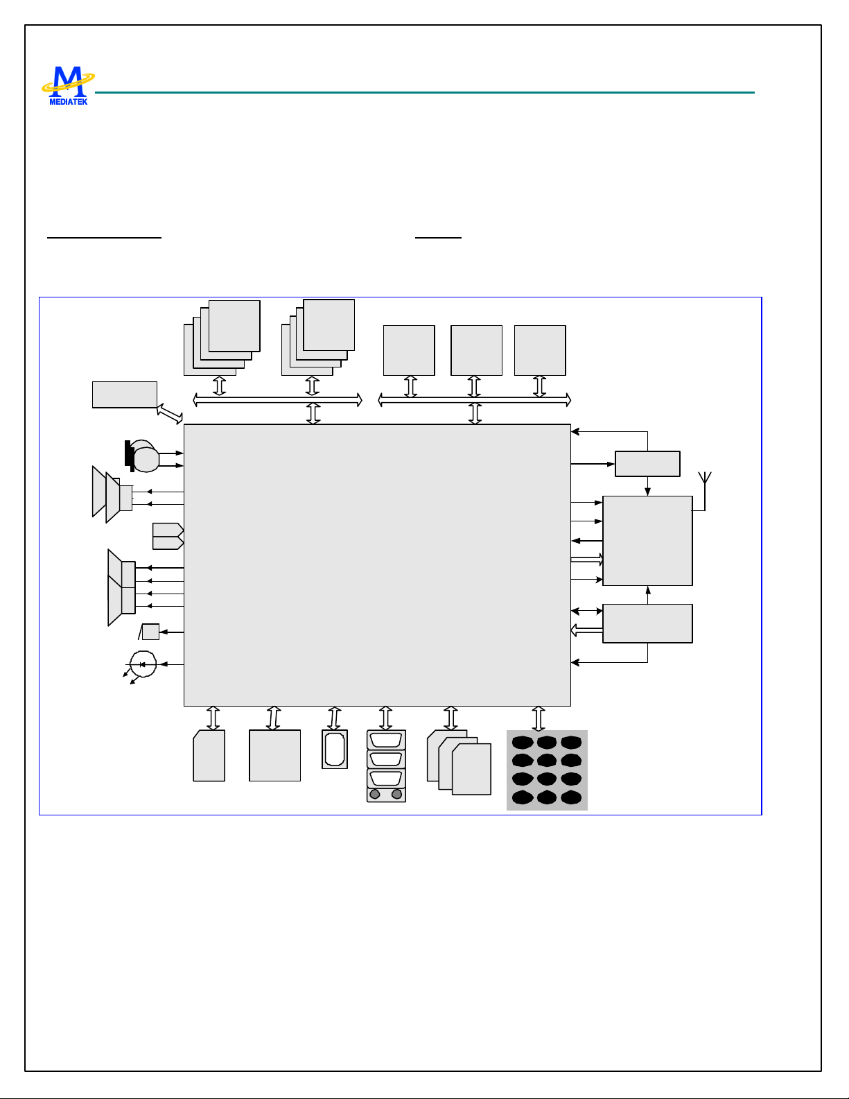
1. System Overview
The MT6217 is a highly integrated single chip solution for
GSM/GPRS phone. Based on 32-bit ARM7EJ-STM RISC
processor, MT6217 features not only high performance
GPRS Class 12 MODEM but is also designed with support
for the wireless multi-media applications, such as
advanced display engine, hardware JPEG decoder,
synthesis audio with 64-tone polyphony, digital audio
playback, Java acceleration, MMS and etc. Additionally,
MT6217 provides varieties of advanced interfaces for
functionality extensions, like 8-port external memory
inte rface, 3-port 8/16-bit parallel interface, NAND Flash,
IrDA, USB and MMC/SD/MS/MS Pro. The typical
application can be shown as Figure 1.
External Memory Interface
Providing the greatest capacity for expansion, the MT6217
supports u p to 8 state-of-the-art devices with SRAM-like
interface, including burst/page mode Flash, page mode
SRAM, Pseudo SRAM, Color/Parallel LCD, and
multi-media companion chip, like Camera and Melody
chips. Regarding the consideration of power consumption
and low noise, this interface is designed for flexible I/O
voltage and allows for lowering supply voltage down to
1.8V. In addition, the driving strength is configurable that
makes the signal integrity problem easy. Retention
technology is also specifically used on data bus to prevent
the bus from being floating during turn over.
Multi-media Subsystem
In order to provide more flexibility and bandwidth for
multi-media products, an additional 8/16 bit parallel
interface is incorporated. This interface is designed
specially for support with Camera companion chip as well
as LCD panel. Moreover, it can connect NAND flash
device to provide a solution for multi-media data storage.
For running multi-media application faster, MT6217
integrates also several hardware-based engines. With
hardware based JPEG decoder, the MT6217 easily handles
real-time playback of compressed image. With hardware
based Resizer and advanced display engine, it can display
and combine arbitrary size of images with up to 4 blending
layers.
User Interface
For user interactions, the MT6217 brings together all
necessary peripheral blocks for multi-media GSM/GPRS
phone. It comprises the Keypad Scanner with capability of
multiple key pressing, SIM Controller, Alerter, Real Time
Clock, PWM, Serial LCD Controller and General Purpose
Programmable I/Os. For connectivity and data storage, the
MT6217 consists of UART, IrDA, USB 1.1 Slave and
MMC/SD/MS/MS Pro. Besides, for large amount of data
transfer, high performance DMA (Direct Memory Access)
and hardware flow control are implemented, that greatly
enhances the performance and saves precious processing
power.
Audio Interface
With highly integrated mixed-signal Audio Front-End, the
MT6217 completes an architecture that allows for easy
audio interfacing with direct connection to the audio
transducers. Not only D/A and A/D Converters for Voice
Band, but also the high resolution Stereo D/A Converters
for Audio band are integrated. In addition, the MT6217
provides also Stereo Input and Analog Mixer. All of them
enable the MT6217 based terminal a rich platform for
multi-media applications.
Radio Interface
Providing a well-organized radio interface with flexibility
for efficient customization, the MT6217 integrates
mixed-signal Baseband Front-End. It carries out gain and
offset calibration mechanisms and filters with
programmable coefficients for comprehensive
compatibility control on RF modules. The approach is also
combining a high resolution D/A Converter for controlling
VCXO or crystal instead of TCVCXO to reduce the
overall system cost. On the other hand, with 14-bit high
resolution A/D Converter for RF downlink path, MT6217
achieves great quality of MODEM performance. Besides,
to remove the necessary of external current-driving
component, the driving strength of some BPI outputs is
designed to be configurable.
Debug Function
6/349 MediaTek Inc. Confidential
MT6217 GSM/GPRS Baseband Processor Data Sheet Revision 1.01
The JTAG interface enables in -circuit debugging of
software program with the ARM7EJ-S core. With this
standardized debugger interface, the MT6217 provides
developers with a wide set of options for choosing ARM
development kits from supports of thirty parties.
Power Management
The MT6217 offers various low-power features helping
reduce system power consumption including Pause Mode
Flash
SRAM
PSRAM
Debugger
JTAG
Speech/Audio
Input
Speech/Audio
Output
FM Stereo
Radio Input
Melody
LCD
External Memory
Interface
MT6217
HiFi Stero
Output
Alerter
of 32KHz clocking at Standby State, Power Down Mode
for individual peripherals and Processor Sleep Mode.
Fabricated in low-power CMOS process, together with the
low-power features, the overall system can achieve ultra
low power consumption.
Package
The MT6217 device is offered in a 1 3mm×13mm, 282-ball,
0.65 mm pitch, TFBGA package.
Camera
NAND
Flash
8/16-bit Parallel
Interface
LCD
SYSCLK
AFC
APC
TX I/Q
RX I/Q
BPI
BSI
B2PSI
AuxAD
TCVCXO
RF
Module
Power
Management
C
Circuitry
PWM
SIM
Serial
LCD
Serial
LCD
USB
UART
IrDA
MMC/SD/MS/
MSPro
Supply Voltages
Keypad
1 2 3
4 5 6
7 8 9
0 #
*
Figure 1 Typical application of MT6217
7/349 MediaTek Inc. Confidential

MT6217 GSM/GPRS Baseband Processor Data Sheet Revision 1.01
1.1 Features
n General
l Integrated voice -band, audio-band and base-band analog front ends
l TFBGA 13mm×13mm, 282-ball, 0.65 mm pitch package
n MCU Subsystem
l ARM7EJ -S 32-bit RISC processor
l Java hardware acceleration for faster Java-based games and other applets
l Operating frequency: 26/52 MHz
l 13 DMA channels
l 128 K Bytes zero -wait-state on-chip SRAM
l On-chip boot ROM for Factory Flash Programming
l Watchdog timer for system crash recovery
l 2 sets of General Purpose Timer
l Circuit Switch Data and Division coprocessors
n External Memory Interface
l Support up to 8 external devices
l Support 8-bit or 16-bit memory components with size up to 64M Bytes each
l Support Flash and SRAM with Page Mode or Burst Mode
l Support Pseudo SRAM
l Industrial standard Parallel LCD Interface
l Built-in hardware acceleration function for color LCD panels
l Support multi-media companion chips with 8/16 bits data width
l Flexible I/O voltage of 1.8V ~ 3V for memory interface
l Configurable driving strength for memory interface
n Multi-media Subsystem
l Dedicated 8/16-bit Parallel Interface, support up to 3 external devices
l High speed hardware JPEG decoder, support both baseline sequential and progressive JPEG files
l High quality hardware Resizer capable of tailoring JPEG image to arbitrary size
l Support simultaneously equipping up to 2 parallel LCD and 1 serial LCD panels
l Support LCD panel maximum resolution up to 800x600 at 16bpp
8/349 MediaTek Inc. Confidential

MT6217 GSM/GPRS Baseband Processor Data Sheet Revision 1.01
l Capable of combining display memories with up to 4 blending layers
l NAND Flash Interface for mass storages
l Full-speed USB 1.1 Device
l Multi Media Card/Secure Digital Memory Card/Memory Stick/Memory Stick Pro controller
n Audio and Modem CODEC
l Wavetable synthesis with up to 64 notes
l Advanced wavetable synthesizer capable of generating simulated stereo
l Wavetable including GM full set of 128 instruments and 47 sets of percussion
l PCM Playback and Record
l Dial tone generation
l Voice Memo
l Noise Reduction
l Echo Suppression
l Advanced Sidetone Oscillation Reduction
l Digital sidetone generator with programmable gain
l Two programmable acoustic compensation filters
l GSM/GPRS quad vocoders for adaptive multirate (AMR), enhanced full rate (EFR), full rate (FR) and half rate (HR)
l GSM channel coding, equalization and A5/1 and A5/2 ciphering
l GPRS GEA and GEA2 ciphering
l Programmable GSM/GPRS Modem
l Packet Switched Data with CS1/CS2/CS3/CS4 coding schemes
l GSM Circuit Switch Data
l GPRS Class 12
n User Interfaces
l 6-row × 7-column keypad controller with hardware scanner
l Support multiple key press for gaming
l SIM Card Controller with hardware flow control
l 3 UARTs with hardware flow control and speed up to 921600 bps
l IrDA modulator/demodulator with hardware framer
l Real Time Clock (RTC) operating with a separate power supply
l Serial LCD Interf ace with 7 bytes TX FIFO
9/349 MediaTek Inc. Confidential

MT6217 GSM/GPRS Baseband Processor Data Sheet Revision 1.01
l General Purpose I/Os (GPIOs)
l 2 Sets of Pulse Width Modulation (PWM) Output
l Alerter Output with Enhanced PWM or PDM
l Six external interrupt lines
n Audio Interface and Audio Front End
l Two microphone inputs sharing one low noise amplifi er with programmable gain
l Two Voice power amplifiers with programmable gain
l 2nd order Sigma -Delta A/D Converter for voice uplink path
l D/A Converter for voice downlink path
l High resolution D/A Converters for Stereo Audio playback
l Stereo analog input for ste reo audio source
l Analog Multiplexer for Stereo Audio
l Stereo to Mono Conversion
l Support half-duplex hands-free operation
l Complying with GSM 03.50
n Radio Interface and Baseband Front End
l GMSK modulator with analog I and Q channel outputs
l 10-bit D/A Converter for uplink baseband I and Q signals
l 14-bit high resolution A/D Converter for downlink baseband I and Q signals
l Calibration mechanism of offset and gain mismatch for baseband A/D Converter and D/A Converter
l 10-bit D/A Converter for Automatic Power Control
l 13-bit high resolution D/A Converter for Automatic Frequency Control
l Programmable Radio RX filter
l 2 Channels Baseband Serial Interface (BSI) with 3-wire control
l 10-Pin Baseband Parallel Interface (BPI) with programmable driving strength
l Multi-band support
n Power Management
l Power Down Mode for analog and digital circuits
l Processor Sleep Mode
l Pause Mode of 32KHz clocking at Standby State
l 7-channel Auxiliary 10-bit A/D Converter for charger and battery monitoring
10/349 MediaTek Inc. Confidential

MT6217 GSM/GPRS Baseband Processor Data Sheet Revision 1.01
n Test and Debug
l Built-in digital and analog loop back modes for both Audio and Baseband Front-End
l DAI port complying with GSM Rec.11.10
l JTAG port for debugging embedded MCU
11/349 MediaTek Inc. Confidential

MT6217 GSM/GPRS Baseband Processor Data Sheet Revision 1.01
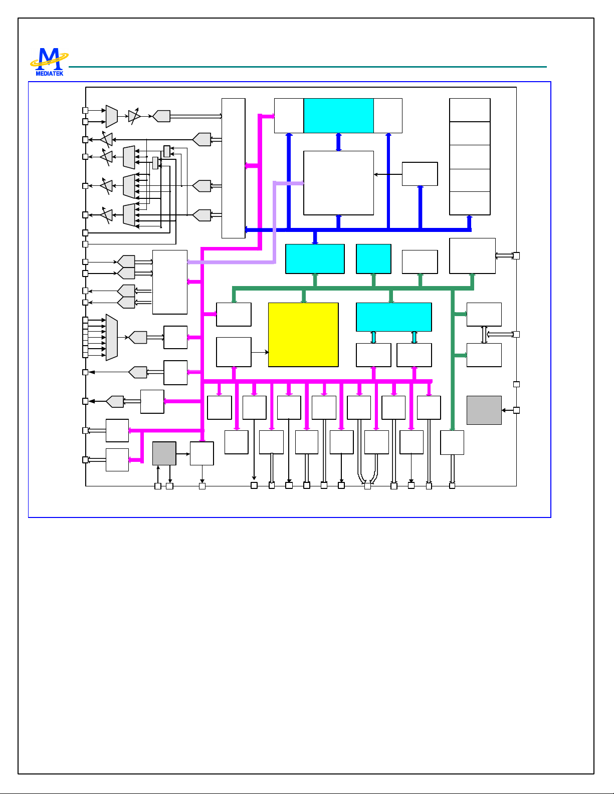
1.2 General Description
Figure 2 details the block diagram of MT6217. Based on dual-processor architecture, the major processor of MT6217 is
ARM7EJ-S, which mainly runs high-level GSM /GPRS protocol software as well as multi-media applications. With the
other one is a digital signal processor corresponding for handling the low-level MODEM as well as advanced audio
functions. Except for some mixed -signal circuitries, the other building blocks in MT6217 are connected to either the
microcontroller or the digital signal processor. Specifically, MT6217 consists of the following subsystems:
l Microcontroller Unit (MCU) Subsystem, including an ARM7EJ -S RISC processor and its accompanying memory
management and interrupt handling logics.
l Digital Signal Processor (DSP) Subsystem, including a DSP and its accompanying memory, memory controller,
and interrupt controller.
l MCU/DSP Interface, where the MCU and the DSP exchange hardware and software information.
l Microcontroller Peripherals, which includes all user interface modules and RF control interface modules.
l Microcontroller Coprocessors, which intends to run computing-intensive processes in place of Microcontroller.
l DSP Peripherals, which are hardware accelerators for GSM /GPRS channel codec.
l Multi-media Subsystem, which integrate several advanced accelerators to support multi-media applications.
l Voice Front End, the data path of conveying analog speech from and to digital speech.
l Audio Front End, also the data path of conveying stereo audio from stereo audio source
l Baseband Front End, the data path of conveying digital signal form and to analog signal of RF modules.
l Timing Generator, generating the control signals related to the TDMA frame timing.
l Power, Reset and Clock subsystem, managing the power, reset and clock distribution inside MT6217.
Details of the individual subsystems and blocks are described in following Chapters.
12/349 MediaTek Inc. Confidential
MT6217 GSM/GPRS Baseband Processor Data Sheet Revision 1.01
MIC_0
MIC_1
VOICE_0
VOICE_1
AUDIO_L
AUDIO_R
STEREO_L
STEREO_R
RX_I
RX_Q
TX_I
TX_Q
Aux
ADC
AFC
APC
Serial RF
Control
Parallel RF
Control
MT6217
ADC
ADC
DAC
DAC
ADC
DAC AFC
DAC APC
BSI
BPI
ADC
+
+
Baseband
Path
Aux
ADC
32K
OSC
DAC
DAC
DAC
RTC
Interrupt
Controller
TDMA
Timer
Audio
Path
Bridge
GPT
WDT
SIM GPIO
Patch
Unit
ARM7EJ-S
PWM
MCU/DSP
Interface
Keypad
Scanner
Memory
DSP
Boot
ROM
Image
Resizer
Serial
LCD
B2PSI IrDA
Trap
Unit
On-Chip
SRAM
MMC
SD/MS
MS Pro
Interrupt
Controller
DMA
Controller
JPEG
Decoder
UART
DSP
Coprocessor
DSP
Coprocessor
DSP
Coprocessor
DSP
Coprocessor
DSP
Coprocessor
External
Memory
Interface
USBAlerter
LCD
Controller
NAND Flash
Controller
Clock
Generator
Flash
SRAM
LCD
Melody
NAND
Flash
LCD
Camera
JTAG
System
Clock
13/26MHz
32KHz
Crystal
Wake Up User InterfaceReset
ConnectivitySerial Port
Figure 2 MT6217 block diagram.
13/349 MediaTek Inc. Confidential

MT6217 GSM/GPRS Baseband Processor Data Sheet Revision 1.01
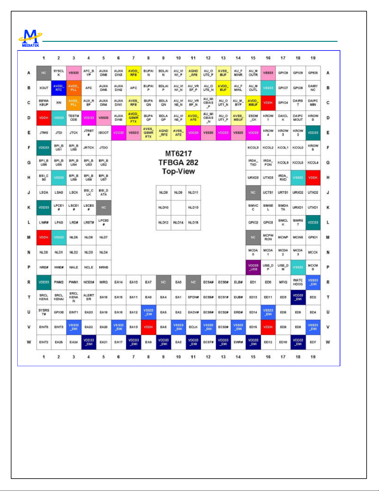
2 Product Description
2.1 Pin Outs
One type of package for this product, TFBGA 13mm*13mm, 282-ball, 0.65 mm pitch Package, is offered.
Pin outs and the top view are illustrated in Figure 3 for this package. Outline and dimension of package is illustrated in
Figure 4, while the definition of package is shown in Table 1.
14/349 MediaTek Inc. Confidential
MT6217 GSM/GPRS Baseband Processor Data Sheet Revision 1.01
Figure 3 Top Vi ew of MT6217 TFBGA 13mm*13mm, 282-ball, 0.65 mm pitch Package
15/349 MediaTek Inc. Confidential

MT6217 GSM/GPRS Baseband Processor Data Sheet Revision 1.01
Figure 4 Outlines and Dimension of TFBGA 13 mm*13mm, 282-ball, 0.65 mm pitch Package
Body Size Ball Count Ball Pitch Ball Dia. Package Thk. Stand Off Substrate Thk.
D E N e b A (Max.) A1 C
13 13 282 0.65 0.3 1.4 0.3 0.36
Table 1 Definition of TFBGA 13mm*13mm, 282-ball, 0.65 mm pitch Package (Unit: mm)
16/349 MediaTek Inc. Confidential
MT6217 GSM/GPRS Baseband Processor Data Sheet Revision 1.01
2.2 Pin Description
Ball
13 X13
Name Dir Description
JTAG Port
E4 JTRST# I
E3 JTCK I
E2 JTDI I
E1 JTMS I
F5 JTDO O
F4 JRTCK O
JTAG test port reset input
JTAG test port clock input
JTAG test port data input
JTAG test port mode switch
JTAG test port data output
JTAG test port returned clock output
RF Parallel Control Unit
F3 BPI_BUS0 O
F2 BPI_BUS1 O
G5 BPI_BUS2 O
G4 BPI_BUS3 O
G3 BPI_BUS4 O
G2 BPI_BUS5 O
G1 BPI_BUS6 IO
H5 BPI_BUS7 IO
H4 BPI_BUS8 IO
H3 BPI_BUS9 IO
RF hard-wire control bus 0
RF hard-wire control bus 1
RF hard-wire control bus 2
RF hard-wire control bus 3
RF hard-wire control bus 4
RF hard-wire control bus 5
RF hard-wire control bus 6 GPIO10 BPI_BU
RF hard-wire control bus 7 GPIO11 BPI_BU
RF hard-wire control bus 8 GPIO12 BPI_BU
RF hard-wire control bus 9 GPIO13 BPI_BU
RF Serial Control Unit
H1 BSI_CS0 O
J5 BSI_DATA O
J4 BSI_CLK O
RF 3-wire interface chip select 0
RF 3-wire interface data output
RF 3-wire interface clock output
PWM Interface
R3 PWM1 IO
R2 PWM2 IO
T4 ALERTER IO
Pulse width modulated signal 1
Pulse width modulated signal 2
Pulse width modulated signal for buzzer
Serial LCD/PM IC Interface
J3 LSCK IO
J2 LSA0 IO
J1 LSDA IO
K4 LSCE0# IO
K3 LSCE1# IO
Serial display interface data output GPIO16 LSCK TBTXE
Serial display int erface address output GPIO17 LSA0 TDTIR
Serial display interface clock output GPIO18 LSDA TCTIR
Serial display interface chip select 0
output
Serial display interface chip select 1 GPIO20 LSCE1# LPCE2# TEVTV
Mode0 Mode1 Mode2 Mode3
Pull Reset
PD Input
PU Input
PU Input
PU Input
0
0
0
0
0
0
0
0
S6
6.5MHz 26MHz
S7
13MHz 26MHz
S8
BSI_CS1
S9
PD Input
PD Input
PD Input
PD Input
0
0
0
GPIO21 PWM1 DSP_G
PO0
GPIO22 PWM2 DSP_G
PO1
GPIO23 ALERT
ER
DSP_G
PO2
TBTX
FS
TBRX
EN
BTRX
FS
PD Input
PD Input
PD Input
PU Input
N
PU Input
Q
PU Input
Q2
GPIO19 LSCE0# DSP_TI
D0
TCTIR
Q1
PU Input
PU Input
17/349 MediaTek Inc. Confidential
MT6217 GSM/GPRS Baseband Processor Data Sheet Revision 1.01
output AL
Parallel LCD/Nand-Flash Interface
K2 LPCE1# IO
L5 LPCE0# O
L4 LRST# O
L3 LRD# O
L2 LPA0 O
L1 LWR# O
L11 NLD15 IO
L10 NLD14 IO
K11 NLD13 IO
L9 NLD12 IO
J11 NLD11 IO
K9 NLD10 IO
J10 NLD9 IO
J9 NLD8 IO
M5 NLD7 IO
M4 NLD6 IO
M3 NLD5 IO
N5 NLD4 IO
N4 NLD3 IO
N3 NLD2 IO
N2 NLD1 IO
N1 NLD0 IO
P5 NRNB IO
P4 NCLE IO
P3 NALE IO
P2 NWE# IO
P1 NRE# IO
R4 NCE0# IO
Parallel display interface chip select 1
output
Parallel display interface chip select 0
output
Parallel display interface Reset Signal
Parallel display interface Read Strobe
Parallel display interface address output
Parallel display interface Write Strobe
Parallel LCD/NAND-Flash Data 15
Parallel LCD/NAND-Flash Data 14
Parallel LCD/NAND-Flash Data 13
Parallel LCD/NAND-Flash Data 12
Parallel LCD/NAND-Flash Data 11
Parallel LCD/NAND-Flash Data 10
Parallel LCD/NAND-Flash Data 9
Parallel LCD/NAND-Flash Data 8
Parallel LCD/NAND-Flash Data 7
Parallel LCD/NAND-Flash Data 6
Parallel LCD/NAND-Flash Data 5
Parallel LCD/NAND-Flash Data 4
Parallel LCD/NAND-Flash Data 3
Parallel LCD/NAND-Flash Data 2
Parallel LCD/NAND-Flash Data 1
Parallel LCD/NAND-Flash Data 0
NAND-Flash Read/Busy Flag GPIO25
NAND-Flash Command Latch Signal GPIO26
NAND-Flash Address Latch Signal GPIO27
NAND-Flash Write Strobe GPIO28
NAND-Flash Read Strobe GPIO29
NAND-Flash Chip select output GPIO30
SIM Card Interf ace
L18 SIMRST O
L17 SIMCLK O
K15 SIMVCC O
K16 SIMSEL IO
SIM card reset output
SIM card clock output
SIM card supply power control
SIM card supply power select
GPIO24 LPCE1# NCE1# MCU_
TD0
PU
PD
PD
PD
PD
PD
PD
PD
PD
PD
PD
PD
PD
PD
PD
PD
PD
NRNB
NCLE
NALE
NWE#
NRE#
NCE0#
DSP_TI
D1
DSP_TI
D2
DSP_TI
D3
DSP_TI
D4
DSP_TI
D5
DSP_TI
D6
MCU_T
ID1
MCU_
TID2
MCU_
TID3
MCU_
DID
MCU_
DFS
MCU_
DCK
PU
PD
PD
PU
PU
PU
0
0
0
GPIO32 SIMSEL PD 0
K17 SIMDATA IO
SIM card data input/output
0
Dedicated GPIO Interface
U2 GPIO0 IO
18/349 MediaTek Inc. Confidential
General purpose input/output 0 GPIO0 DSP_GP
O3
PD Input
MT6217 GSM/GPRS Baseband Processor Data Sheet Revision 1.01
M19 GPIO1 IO
L15 GPIO2 IO
L16 GPIO3 IO
C17 GPIO4 IO
A19 GPIO5 IO
B18 GPIO6 IO
B17 GPIO7 IO
A18 GPIO8 IO
A17 GPIO9 IO
Miscellaneous
U1 SYSRST# I
R18 WATCHD
O
OG#
T3 SRCLKEN
O
AN
T1 SRCLKENA O
T2 SRCLKEN
IO
AI
D3 TESTMODE I
General purpose input/output 1 GPIO1 DICK
General purpose input/output 2 GPIO2 DID
General purpose input/output 3 GPIO3 DIMS
General purpose input/output 4 GPIO4 DSP_CKL DSPLCK TRASD
4
General purpose input/output 5 GPIO5 AHB_C
LK
General purpose input/output 6 GPIO6 ARM_C
LK
General purpose input/output 7 GPIO7 SLOW_
CK
General purpose input/output 19 GPIO8 F32K_CK DSPLD0 TRASD
General purpose input/output 21 GPIO9 TRARS
System reset input active low
Watchdog reset output
External TCXO enable output active low
External TCXO enable output active
high
External TCXO enable input
Test Mode control input
Input
1
GPO1
GPO0
GPIO31
SRCLK
ENAN
SRCLK
ENA
SRCLK
ENAI
DSPLD3 TRASD
3
DSPLD2 TRASD
2
DSPLD1 TRASD
1
0
YNC
0
1
PD
PD
PD Input
PD Input
PD Input
PD Input
PD Input
PD Input
PD Input
PD Input
PD Input
D15 ESDM_CK O
E5 IBOOT I
Keypad Interface
G17 KCOL6 I
G18 KCOL5 I
G19 KCOL4 I
F15 KCOL3 I
F16 KCOL2 I
F17 KCOL1 I
F18 KCOL0 I
F19 KROW5 O
E16 KROW4 O
E17 KROW3 O
E18 KROW2 O
D16 KROW1 O
D19 KROW0 O
External Interrupt Interface
V1 EINT0 I
U3 EINT1 I
W1 EINT2 I
Internal monitor clock output
Boot Device Configuration Input
Keypad column 6
Keypad column 5
Keypad column 4
Keypad column 3
Keypad column 2
Keypad column 1
Keypad column 0
Keypad row 5
Keypad row 4
Keypad row 3
Keypad row 2
Keypad row 1
Keypad row 0
External interrupt 0
External interrupt 1
External interrupt 2
Input
PU Input
PU Input
PU Input
PU Input
PU Input
PU Input
PU Input
0
0
0
0
0
0
N.C.
PU Input
PU Input
PU Input
19/349 MediaTek Inc. Confidential
MT6217 GSM/GPRS Baseband Processor Data Sheet Revision 1.01
V2 EINT3 I
R5 MIRQ IO
R17 MFIQ IO
External interrupt 3
Interrupt to MCU GPIO41 MIRQ 13MHz 6.5MHz
Interrupt to MCU GPIO42 MFIQ
External Memory Interface
R16 ED0 IO
R15 ED1 IO
T19 ED2 IO
T17 ED3 IO
U19 ED4 IO
U18 ED5 IO
V18 ED6 IO
W19 ED7 IO
U17 ED8 IO
V17 ED9 IO
W17 ED10 IO
T16 ED11 IO
W16 ED12 IO
T15 ED13 IO
U15 ED14 IO
V15 ED15 IO
U14 ERD# O
W14 EWR# O
R13 ECS0# O
T13 ECS1# O
U13 ECS2# O
V13 ECS3# O
R12 ECS4# O
T12 ECS5# O
U12 ECS6# O
W12 ECS7# IO
R14 ELB# O
T14 EUB# O
External memory data bus 0
External memory data bus 1
External memory data bus 2
External memory data bus 3
External memory data bus 4
External memory data bus 5
External memory data bus 6
External memory data bus 7
External memory data bus 8
External memory data bus 9
External memory data bus 10
External memory data bus 11
External memory data bus 12
External memory data bus 13
External memory data bus 14
External memory data bus 15
External memory read strobe
External memory write strobe
External memory chip select 0
External memory chip select 1
External memory chip select 2
External memory chip select 3
External memory chip select 4
External memory chip select 5
External memory chip select 6
External memory chip select 7
External memory lower byte strobe
External memory upper byte strobe
PU Input
PU Input
PU Input
PU/
PD
PU/
PD
PU/
PD
PU/
PD
PU/
PD
PU/
PD
PU/
PD
PU/
PD
PU/
PD
PU/
PD
PU/
PD
PU/
PD
PU/
PD
PU/
PD
PU/
PD
PU/
PD
1
1
1
1
1
1
1
1
1
GPIO40 ECS7# PU 1
1
1
Input
Input
Input
Input
Input
Input
Input
Input
Input
Input
Input
Input
Input
Input
Input
Input
20/349 MediaTek Inc. Confidential
MT6217 GSM/GPRS Baseband Processor Data Sheet Revision 1.01
T11 EPDN# O
U11 EADV# O
V11 ECLK O
R10 EA0 O
T10 EA1 O
U10 EA2 O
W10 EA3 O
T9 EA4 O
U9 EA5 O
V9 EA6 O
R8 EA7 O
T8 EA8 O
W8 EA9 O
R7 EA10 O
T7 EA11 O
U7 EA12 O
V7 EA13 O
R6 EA14 O
T6 EA15 O
U6 EA16 O
W6 EA17 O
T5 EA18 O
U5 EA19 O
V5 EA20 O
W5 EA21 O
V4 EA22 O
U4 EA23 O
W3 EA24 O
W2 EA25 O
USB Interface
P16 USB_DP IO
P17 USB_DM IO
Memory Card Interface
P19 MCCM0 IO
N15 MCDA0 IO
N16 MCDA1 IO
N17 MCDA2 IO
N18 MCDA3 IO
N19 MCCK O
M16 MCPWRO O
Power Down Control Signal for PSRAM
Address valid for burst mode flash
memory
Clock for flash memory
External memory ad dress bus 0
External memory address bus 1
External memory address bus 2
External memory address bus 3
External memory address bus 4
External memory address bus 5
External memory address bus 6
External memory address bus 7
External memory address bus 8
External memory address bus 9
External memory address bus 10
External memory address bus 11
External memory address bus 12
External memory address bus 13
External memory address bus 14
External memory address bus 15
External memory ad dress bus 16
External memory address bus 17
External memory address bus 18
External memory address bus 19
External memory address bus 20
External memory address bus 21
External memory address bus 22
External memory address bus 23
External memory address bus 24
External memory address bus 25
USB D+ Input/Output
USB D- Input/Output
SD Command/MS Bus State Output
SD Serial Data IO 0/MS Serial Data IO
SD Serial Data IO 1
SD Serial Data IO 2
SD Serial Data IO 3
SD Serial Clock/MS Serial Clock Output
SD Power On Control Output
GPO2 EPDN# 0
1
0
0
0
0
0
0
0
0
0
0
0
0
0
0
0
0
0
0
0
0
0
0
0
0
0
0
0
PU/
PD
PU/
PD
PU/
PD
PU/
PD
PU/
PD
21/349 MediaTek Inc. Confidential
MT6217 GSM/GPRS Baseband Processor Data Sheet Revision 1.01
N
M17 MCWP I
M18 MCINS I
UART Interface
K18 URXD1 I
K19 UTXD1 O
J16 UCTS1 I
J17 URTS1 O
J18 URXD2 IO
J19 UTXD2 IO
H15 URXD3 IO
H16 UTXD3 IO
H17 IRDA_RXD IO
G15 IRDA_TXD IO
G16 IRDA_PDN IO
Digital Audio Interface
D17 DAICLK IO
D18 DAIPCM O
IO
UT
C19 DAIPCMIN IO
C18 DAIRST IO
B19 DAISYNC IO
SD Write Protect Input GPIO15 MCWP
SD Card Detect Inp ut GPIO14 MCINS
UART 1 receive data PU Input
UART 1 transmit data 1
UART 1 clear to send PU Input
UART 1 request to send 1
UART 2 receive data GPIO35 URXD2 UCTS3 PU Input
UART 2 transmit data GPIO36 UTXD2 URTS3 PU Input
UART 3 receive data GPIO33 URXD3 PU Input
UART 3 transmit data GPIO34 UTXD3 PU Input
IrDA receive data GPIO37 IRDA_R
XD
IrDA transmit data GPIO38 IRDA_T
XD
IrDA Power Down Control GPIO39 IRDA_P
DN
DAI clock output GPIO43 DAICLK TDMA_
DAI pcm data out GPIO44 DAIPC
MOUT
DAI pcm data input GPIO45 DAIPC
MIN
DAI reset signal input GPIO47 DAIRST TDMA_
DAI frame synchronizat ion signal output GPIO46 DAISYNC BFEPRBO TRASD5 PU Input
UCTS2 PU Input
URTS2 PU Input
PU Input
TRACLK PU Input
CK
TDMA_
D1
TDMA_
D2
FS
TRASY
NC
TRASD7 PU Input
TRASD6 PU Input
PU
PU
PD Input
Analog Interface
B15 AU_MOUL
A15 AU_MOUR
C14 AU_M_BYP
B14 AU_FMINL
A14 AU_FMINR
D13 AU_OUT1_P
C13 AU_OUT1_N
B12 AU_OUT0_N
A12 AU_OUT0_P
C12 AU_MICBI
Audio analog output left channel
Audio analog output right channel
Audio DAC bypass pin
FM radio analog input left channel
FM radio analog input right channel
Earphone 1 amplifier output (+)
Earphone 1 amplifier output (-)
Earphone 0 amplifier output (-)
Earphone 0 amplifier output (+)
Microphone bias supply (+)
AS_P
D12 AU_MICBI
22/349 MediaTek Inc. Confidential
Microphone bias supply (-)
MT6217 GSM/GPRS Baseband Processor Data Sheet Revision 1.01
AS_N
C11 AU_VREF_N
Audio reference voltage (-)
B11 AU_VREF_P
D10 AU_VIN0_P
C10 AU_VIN0_N
B10 AU_VIN1_N
A10 AU_VIN1_P
D9 BDLAQP
C9 BDLAQN
A9 BDLAIN
B9 BDLAIP
B8 BUPAIP
A8 BUPAIN
C8 BUPAQN
D8 BUPAQP
B7 APC
D6 AUXADIN
Audio reference voltage (+)
Microphone 0 amplifier input (+)
Microphone 0 amplifier input (-)
Microphone 1 amplifier input (-)
Microphone 1 amplifier input (+)
Quadrature input (Q+) baseband code c
downlink
Quadrature input (Q-) baseband codec
downlink
In-phase input (I+) baseband codec
downlink
In-phase input (I-) baseband codec
downlink
In-phase output (I+) baseband codec
uplink
In-phase output (I-) baseband codec
uplink
Quadrature output (Q+) baseband codec
uplink
Quadrature output (Q -) baseband codec
uplink
Automatic power control DAC output
Auxiliary ADC input 0
0
C6 AUXADIN
Auxiliary ADC input 1
1
B6 AUXADIN
Auxiliary ADC input 2
2
A6 AUXADIN
Auxiliary ADC input 3
3
C5 AUXADIN
Auxiliary ADC input 4
4
B5 AUXADIN
Auxiliary ADC input 5
5
A5 AUXADIN
Auxiliary ADC input 6
6
C4 AUX_REF
B4 AFC
A4 AFC_BYP
Auxiliary ADC reference voltage input
Automatic frequency control DAC
output
Automatic frequency control DAC
bypass capacitance
VCXO Interface
A2 SYSCLK
13MHz or 26MHz system clock input
23/349 MediaTek Inc. Confidential
MT6217 GSM/GPRS Baseband Processor Data Sheet Revision 1.01
RTC Interface
C2 XIN
B1 XOUT
C1 BBWAKEUP O
Supply Voltages
D1 VDDK
M1 VDDK
V8 VDDK
V16 VDDK
H19 VDDK
C16 VDDK
W4 VDD33_E
MI
W7 VDD33_E
MI
W9 VDD33_E
MI
W11 VDD33_E
MI
W13 VDD33_E
MI
W15 VDD33_E
MI
W18 VDD33_E
MI
T18 VDD33_E
MI
V3 VSS33_EMI
32.768 KHz crystal input
32.768 KHz crystal output
Baseband power on/off control
Supply voltage of internal logic
Supply voltage of internal logic
Supply voltage of internal logic
Supply voltage of internal logic
Supply voltage of internal logic
Supply voltage of internal logic
Supply voltage of memory interface
driver
Supply voltage of memory interface
driver
Supply voltage of memory interface
driver
Supply voltage of memory interface
driver
Supply voltage of memory interface
driver
Supply voltage of memory interface
driver
Supply voltage of memory interface
driver
Supply voltage of memory interface
driver
Ground of memory interface driver
1
V6 VSS33_EMI
U8 VSS33_EMI
V10 VSS33_EMI
V12 VSS33_EMI
V14 VSS33_EMI
U16 VSS33_EMI
V19 VSS33_EMI
R19 VSS33_EMI
P15 VDD33_US
Ground of memory interface driver
Ground of memory interface driver
Ground of memory interface driver
Ground of memory interface driver
Ground of memory interface driver
Ground of memory interface driver
Ground of memory interface driver
Ground of memory interface driver
Supply voltage of drivers for USB
B
24/349 MediaTek Inc. Confidential
MT6217 GSM/GPRS Baseband Processor Data Sheet Revision 1.01
D4 VDD33
F1 VDD33
K1 VDD33
R1 VDD33
L19 VDD33
E19 VDD33
E15 VDD33
E13 VDD33
E11 VDD33
E6 VDD33
A3 VSS33
D2 VSS33
D5 VSS33
H2 VSS33
M2 VSS33
P18 VSS33
H18 VSS33
A16 VSS33
B16 VSS33
E14 VSS33
E12 VSS33
E7 VSS33
B3 AVDD_PLL
Supply voltage of drivers except
memory interface and USB
Supply voltage of drivers except
memory interface and USB
Supply voltage of drivers except
memory interface and USB
Supply voltage of drivers except
memory interface and USB
Supply voltage of drivers except
memory interface and USB
Supply voltage of drivers except
memory interface and USB
Supply voltage of drivers except
memory interface and USB
Supply voltage of drivers except
memory interface and USB
Supply voltage of drivers except
memory interface and USB
Supply voltage of drivers except
memory interface and USB
Ground of drivers except memory
interface
Ground of drivers except memory
interface
Ground of drivers except memory
interface
Ground of drivers except memory
interface
Ground of drivers except memory
interface
Ground of drivers except memory
interface
Ground of drivers except memory
interface
Ground of drivers except memory
interface
Ground of drivers except memory
interface
Ground of drivers except memory
interface
Ground of drivers except memory
interface
Ground of drivers except memory
interface
Supply voltage for PLL
C3 AVSS_PLL
B2 AVDD_RTC
Ground for PLL supply
Supply voltage for Real Time Clock
Analog Supplies
C15 AVDD_MB
Supply Voltage for Audio band section
UF
25/349 MediaTek Inc. Confidential
MT6217 GSM/GPRS Baseband Processor Data Sheet Revision 1.01
D14 AVSS_MB
UF
B13 AVDD_BUF
A13 AVSS_BUF
D11 AVDD_AFE
A11 AGND_AFE
E10 AVSS_AFE
E9 AGND_RFE
E8 AVSS_GS
MRFTX
D7 AVDD_GS
MRFTX
C7 AVSS_RFE
A7 AVDD_RFE
GND for Audio band section
Supply voltage for voice band transmit
section
GND for voice band transmit section
Supply voltage for voice band receive
section
GND reference voltage for voice band
section
GND for voice band receive section
GND reference voltage for baseband
section, APC, AFC and AUXADC
GND for baseband transmit section
Supply voltage for baseband transmit
section
GND for baseband receive section, APC,
AFC and AUXADC
Supply voltage for baseband receive
section, APC, AFC and AUXADC
Table 2 Pin Descriptions (Bolded types are functions at reset)
26/349 MediaTek Inc. Confidential
MT6217 GSM/GPRS Baseband Processor Data Sheet Revision 1.01
2.3 Power Description
Ball
13X13
B17 GPIO7 VDDK VSSK
A18 GPIO8 VDDK VSSK
A17 GPIO9
B16 VSS33
A16 VSS33
C16 VDDK Typ. 1.8V
E15 VDD33 Typ. 2.8V
D15 ESDM_CK VDD33 VSS33 VDDK VSSK
E14 VSS33
E13 VDD33 Typ. 2.8V
E12 VSS33
E11 VDD33 Typ. 2.8V
E7 VSS33
J9 NLD8
J10 NLD9
K9 NLD10
J11 NLD11
E6 VDD33 Typ. 2.8V
L9 NLD12
K11 NLD13
Name IO Suppl y IO GND Core Supply Core GND Remark
VDD33 VSS33
VDDK VSSK
VDD33 VSS33 VDDK VSSK
VDD33 VSS33 VDDK VSSK
L10 NLD14
L11 NLD15
D5 VSS33
D4 VDD33 Typ. 2.8V
A3 VSS33
B3 AVDD_PLL Typ. 2.8V
A2 SYSCLK AVDD_PLL AVSS_PLL AVDD_PLL AVSS_PLL
C3 AVSS_PLL
B2 AVDD_RTC Typ. 1.5V
B1 XOUT AVDD_RTC VSS33 AVDD_RTC VSS33
C2 XIN AVDD_RTC VSS33 AVDD_RTC VSS33
C1 BBWAKEUP AVDD_RTC VSS33 AVDD_RTC VSS33
D2 VSS33
D3 TESTMODE VDD33 VSS33 VDDK VSSK
D1 VDDK Typ. 1.8V
27/349 MediaTek Inc. Confidential
MT6217 GSM/GPRS Baseband Processor Data Sheet Revision 1.01
E5 IBOOT VDDK VSSK
VDD33 VSS33
E4 JTRST# VDDK VSSK
E3 JTCK VDDK VSSK
E2 JTDI VDDK VSSK
E1 JTMS VDDK VSSK
F5 JTDO VDDK VSSK
F4 JRTCK VDDK VSSK
F3 BPI_BUS0 VDDK VSSK
F2 BPI_BUS1
VDDK VSSK
F1 VDD33 Typ. 2.8V
G5 BPI_BUS2 VDDK VSSK
VDD33 VSS33
G4 BPI_BUS3 VDDK VSSK
G3 BPI_BUS4 VDDK VSSK
G2 BPI_BUS5 VDDK VSSK
G1 BPI_BUS6 VDDK VSSK
H5 BPI_BUS7 VDDK VSSK
H4 BPI_BUS8
VDDK VSSK
H2 VSS33
H3 BPI_BUS9 VDDK VSSK
VDD33 VSS33
H1 BSI_CS0 VDDK VSSK
J5 BSI_DATA VDDK VSSK
J4 BSI_CLK VDDK VSSK
J3 LSCK VDDK VSSK
J2 LSA0 VDDK VSSK
J1 LSDA VDDK VSSK
K4 LSCE0# VDDK VSSK
K3 LSCE1#
VDDK VSSK
K1 VDD33
K2 LPCE1# VDDK VSSK
VDD33 VSS33
L5 LPCE0# VDDK VSSK
L4 LRST# VDDK VSSK
L3 LRD# VDDK VSSK
L2 LPA0 VDDK VSSK
L1 LWR# VDDK VSSK
M5 NLD7 VDDK VSSK
M4 NLD6 VDDK VSSK
M3 NLD5
VDDK VSSK
M2 VSS33
M1 VDDK Typ. 1.8V
28/349 MediaTek Inc. Confidential
MT6217 GSM/GPRS Baseband Processor Data Sheet Revision 1.01
N5 NLD4 VDDK VSSK
VDD33 VSS33
N4 NLD3 VDDK VSSK
N3 NLD2 VDDK VSSK
N2 NLD1 VDDK VSSK
N1 NLD0 VDDK VSSK
P5 NRNB VDDK VSSK
P4 NCLE VDDK VSSK
P3 NALE VDDK VSSK
P2 NEW# VDDK VSSK
P1 NRE# VDDK VSSK
R4 NCE#
VDDK VSSK
R1 VDD33 Typ. 2.8V
R3 PWM1 VDDK VSSK
VDD33 VSS33
R2 PWM2 VDDK VSSK
T4 ALERTER VDDK VSSK
T1 SRCLKENA VDDK VSSK
T3 SRCLKENAN VDDK VSSK
T2 SRCLKENAI VDDK VSSK
U1 SYSRST# VDDK VSSK
U2 GPIO0 VDDK VSSK
V1 EINT0 VDDK VSSK
U3 EINT1 VDDK VSSK
W1 EINT2 VDDK VSSK
V2 EINT3
VDDK VSSK
V3 VSS33_EMI
W2 EA25 VDDK VSSK
W3 EA24 VDDK VSSK
VDD33_EMI VSS33_EMI
U4 EA23 VDDK VSSK
V4 EA22
VDDK VSSK
W4 VDD33_EMI Typ. 1.8~2.8V
R5 MIRQ VDDK VSSK
W5 EA21 VDDK VSSK
VDD33_EMI VSS33_EMI
V5 EA20 VDDK VSSK
U5 EA19 VDDK VSSK
T6 EA18
VDDK VSSK
V6 VSS33_EMI
W6 EA17 VDDK VSSK
U6 EA16 VDDK VSSK
T6 EA15
VDD33_EMI VSS33_EMI
VDDK VSSK
29/349 MediaTek Inc. Confidential
MT6217 GSM/GPRS Baseband Processor Data Sheet Revision 1.01
R6 EA14 VDDK VSSK
W7 VDD33_EMI Typ. 1.8~2.8V
V7 EA13 VDDK VSSK
VDD33_EMI VSS33_EMI
U7 EA12 VDDK VSSK
T7 EA11 VDDK VSSK
R7 EA10
VDDK VSSK
V8 VDDK Typ. 1.8V
U8 VSS33_EMI
W8 EA9 VDDK VSSK
T8 EA8 VDDK VSSK
VDD33_EMI VSS33_EMI
R8 EA7 VDDK VSSK
V9 EA6
VDDK VSSK
W9 VDD33_EMI Typ. 1.8~2.8V
U9 EA5 VDDK VSSK
T9 EA4 VDDK VSSK
W10 EA3
VDD33_EMI VSS33_EMI
VDDK VSSK
V10 VSS33_EMI
U10 EA2 VDDK VSSK
VDD33_EMI VSS33_EMI
T10 EA1 VDDK VSSK
R10 EA0
VDDK VSSK
W11 VDD33_EMI Typ. 1.8~2.8V
U11 EADV# VDDK VSSK
VDD33_EMI VSS33_EMI
V11 ECLK VDDK VSSK
T11 EPDN#
VDDK VSSK
V12 VSS33_EMI
W12 ECS7# VDDK VSSK
VDD33_EMI VSS33_EMI
U12 ECS6# VDDK VSSK
T12 ECS5# VDDK VSSK
R12 ECS4#
VDDK VSSK
W13 VDD33_EMI Typ. 1.8~2.8V
V13 ECS3# VDDK VSSK
U13 ECS2# VDDK VSSK
VDD33_EMI VSS33_EMI
T13 ECS1# VDDK VSSK
R13 ECS0#
VDDK VSSK
V14 VSS33_EMI
W14 EWR# VDDK VSSK
U14 ERD# VDDK VSSK
VDD33_EMI VSS33_EMI
T14 EUB# VDDK VSSK
R14 ELB#
30/349 MediaTek Inc. Confidential
VDDK VSSK
 Loading...