


MX-7930/31/32
MX-7930/31/32 Technical Manual
Section 2 – MX -7930/31/32 Specifications
Issue 1
Contents
Contents..................................................................................................................................1
1. Preface.............................................................................................................................3
1.1 Basic problem..........................................................................................................3
2. The resistor ID ...............................................................................................................3
2.1 The design................................................................................................................3
3. Preface.............................................................................................................................5
4. Accessory interface.....................................................................................................5
5. Signal description.........................................................................................................6
5.1 System connector....................................................................................................6
5.1.1 Signal description..............................................................................................6
5.1.2 Signal levels.......................................................................................................7
6. AX-705/706/707 Travel Charger.................................................................................8
6.1 Temperature ranges................................................................................................8
6.2 Electrical requirements...........................................................................................8
6.2.1 Input frequency..................................................................................................8
6.2.2 Output requirements..........................................................................................8
6.2.3 Output characteristics.......................................................................................8
6.3 Output peak current..............................................................................................10
6.4 System Connector................................................................................................10
6.5 Mechanical details................................................................................................10
7. AX-721 Car charger...................................................................................................11
7.1 Temperature ranges.............................................................................................11
7.2 Weight....................................................................................................................11
7.3 Electrical specification.........................................................................................11
7.3.1 Output requirements........................................................................................11
7.3.2 Input requirements...........................................................................................11
7.3.3 Output current..................................................................................................11
7.4 Output peak current..............................................................................................12
7.5 System Connector................................................................................................12
8. AX-772 Data/fax cable...............................................................................................13
8.1 Block diagram for AX-772...................................................................................13
8.2 ACC_DET :...........................................................................................................13
8.3 Mechanical............................................................................................................14
8.3.1 DB-9 plug.........................................................................................................14
8.3.2 System plug.....................................................................................................14
8.3.3 Cable Data:......................................................................................................14
8.3.4 Electrical Data.................................................................................................15
8.3.5 Phone interface:...............................................................................................15
8.3.6 RS-232 interface:.............................................................................................15
9. AX-773 USB cable. .....................................................................................................16
Page 2. 1
Technical Manual
Issue 1
November 2002

MX-7930/31/32
9.1 Diagram for AX-773.............................................................................................16
9.2 Electrical interface................................................................................................17
9.2.1 Interface to PC.................................................................................................17
9.3 Summary ................................................................................................................18
9.3.1 Cable delay......................................................................................................18
10. Battery- pack 550mAh ..........................................................................................19
10.1 Electrical specification.........................................................................................19
10.2 Temperature:.........................................................................................................19
10.3 Storage Temperature:..........................................................................................19
10.4 Applicable documents..........................................................................................19
10.5 Protection circuit...................................................................................................20
10.5.1 Feature Description.........................................................................................20
10.5.2 Overcharge Voltage Protection.......................................................................20
10.5.3 Over discharge Voltage Protection..................................................................20
10.5.4 Overcharge Current Protection.......................................................................20
10.5.5 Over discharge Current Protection.................................................................20
10.5.6 Short Circuit Protection...................................................................................20
10.5.7 Current Consumption......................................................................................20
11. Battery- pack 900mAh ..........................................................................................21
11.1 Electrical specification.........................................................................................21
11.2 Temperature:.........................................................................................................21
11.3 Storage Temperature:..........................................................................................21
11.4 Applicable documents..........................................................................................21
11.5 Protection circuit...................................................................................................22
11.5.1 Feature Description.........................................................................................22
11.5.2 Overcharge Voltage Protection.......................................................................22
11.5.3 Over discharge Voltage Protection..................................................................22
11.5.4 Overcharge Current Protection.......................................................................22
11.5.5 Over discharge Current Protection.................................................................22
11.5.6 Short Circuit Protection...................................................................................22
11.5.7 Current Consumption......................................................................................22
12. Portable hands free AX-790................................................................................23
12.1 Earphone...............................................................................................................23
12.2 Microphone............................................................................................................24
13. Terms and abbreviations.....................................................................................26
Page 2. 2
Technical Manual
Issue 1
November 2002
MX-7930/31/32
1. Preface
The purpose of this section is to define the interface between the MX-7930/31/32 and its
accessories. This is done to keep the number of different id resistors low (for avoiding a
wrong detection of an accessory) and to make it possible to develop new accessories after
the phone is in MP.
1.1 Basic problem
When using only a resistor for id of accessories, the number of different accessories is very
limited and when it is possible to combine different accessories, the number is even lower
(resistors in parallel). When combining the id resistor with a fixed start-up protocol the number
of possible accessories is almost unlimited.
2. The resistor ID
The purpose of the resistor ID is to determine the type of accessory attached to the phone.
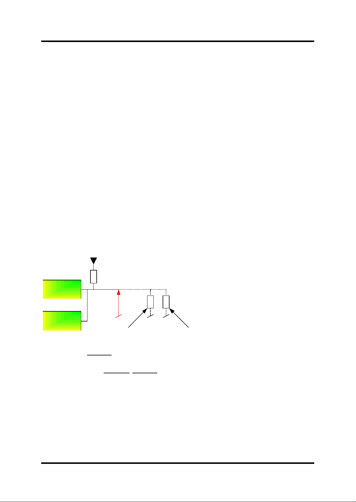
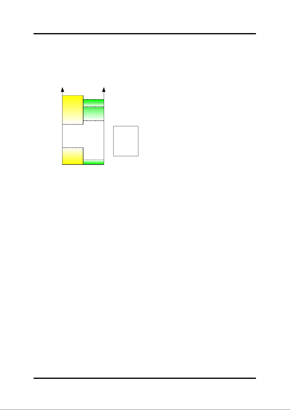
2.1 The design
Figure 2-1 shows the design of the RID. The left side of the figure (from V
inside the Sirius with the reference resistor RS. The codec (ADI: AD6521) measures the V
and thereby makes an identification of the device possible. I f connecting two devices to the
SMX-7930/31/32 e.g. AX-772 (Data-fax cable) their different RID becomes parallel. When the
identification of the accessory has finished (measuring of the RID), it is possible to use the line
as an ordinary I/O. The equations below Figure 2-1 are used for the calculations of the
system. Notice that equation (2) only is valid for 10-bit ADC.
V
REF
) is the circuit
ADC
ADC
AD6521
S
R
10bit ADC
AD6522
I/O
Device 1
Figure 2-1: The RID design.
R
(1)
(2)
VV+=
REFADC
ID
RR
SID
V
2reading ADC
REF10
V
ADC,MAX
V
ADC
ID
ID
R
R
Device 2
R
ID
⋅⋅=
RR
+
SID
Page 2. 3
Technical Manual
Issue 1
November 2002
MX-7930/31/32
Table 2-1 shows the chosen RID and its possible co mbinations for MX-7930/31/32
accessories. The corresponding ADC value is calculated from equation (2) with a ±4%
tolerance. To decode the accessory category refer to Table 2-2.
RID
Accessor
y
68 kΩ A
22 kΩ B
13 kΩ C
47 kΩ D
82 kΩ E
Table 2-1: RID tabel for MX-7930/31/32.
Note: * This is not an error. The V
V
are proportional! Refer to equation (1) and (2).
ADC
Accessory
category
Description Device
A USB cable AX-771
Datafax cable (DTR
B
C
D
LOW)
Datafax cable (DTR
HIGH)
Gernie cable
E Car-kit AX-791
Table 2-2: Accessory category.
VADC [mV] ADC readings
Min Typ Max Min Typ. Max
1,54
4 V
0,81
5 V
0,54
3 V
1,29
6 V
1,66
6 V
1,59
5 V
0,84
6 V
0,57
1 V
1,34
1 V
1,71
9 V
1,640 V 129
0 1306 1321
0,875
V 681 693 705
0,586
V 453 468 472
1,382 V 108
3 1099 1113
1,766 V 139
2
inside the code will compensate this value. V
ADC
Number
AX-770
1408 1422 30
Description
For debugging of phone
Data fax cable
AX770
None
Debug cable
Car-kit
Typ. span
down
31
24
19
30
REF
and
Page 2. 4
Technical Manual
Issue 1
November 2002
MX-7930/31/32
3. Preface
The purpose of this section is to give an overview of the signals on the system connector of
the MX-7930/31/32 wh en the phone is used with various accessories. For a full description of
the signals, refer to the documents of each of the devices. The signal type is oriented from the
phone e.g. when a signal is type ‘I’ (I nput) the signal is an input to the phone and therefore an
output of the device.
4. Accessory interface
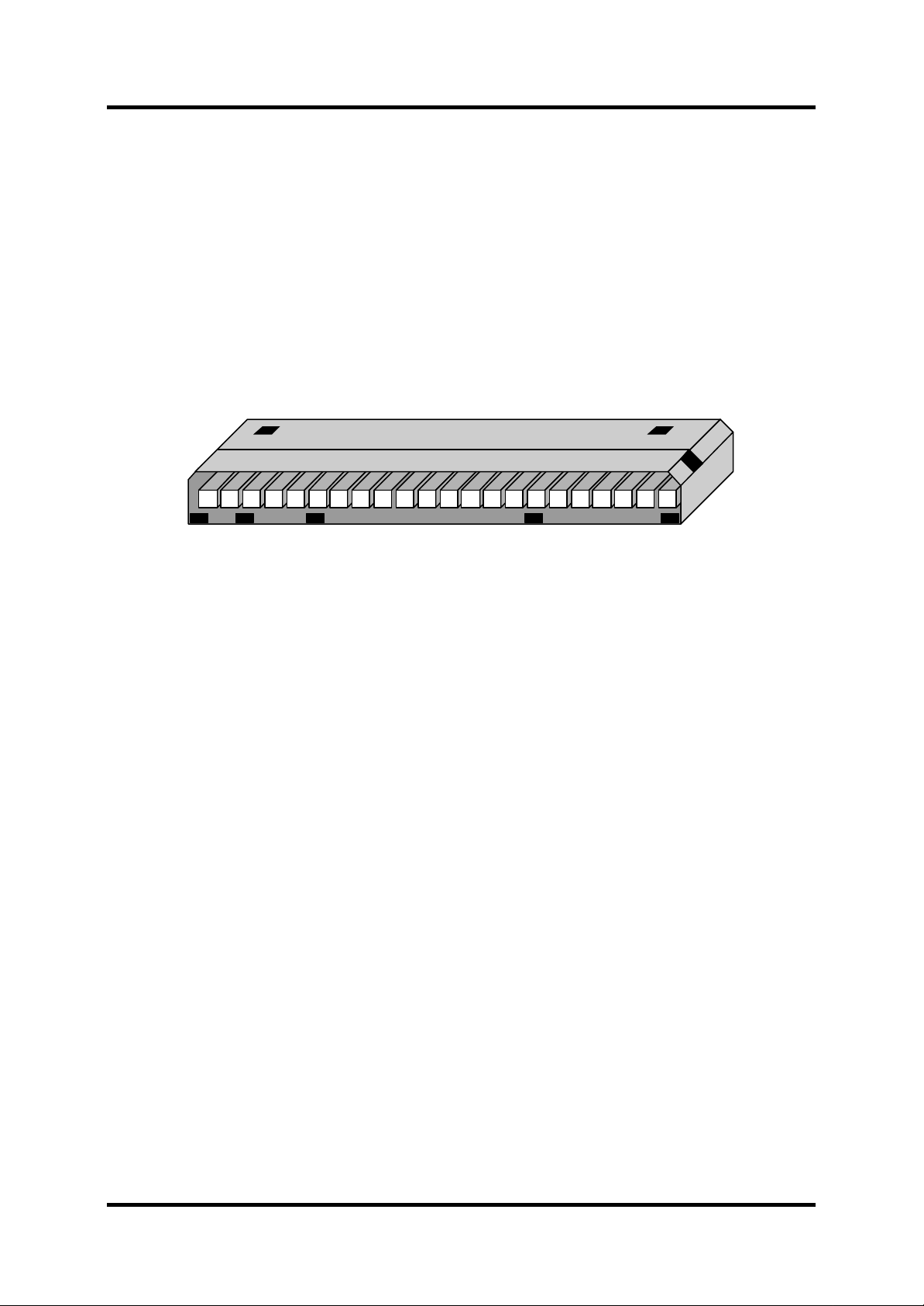
Figure 4-1 is an illustration of the system connector mounted in the phone. The numbers on
the drawing shows the pin numbering of the connector.
Table 4-1 gives an overview of the signal names that appears on the system co nnector when
combining the phone with an acce ssory.
10 8 7 345 126922 20 19 11151617 1213141821
Figure 4-1: The system connector insight the phone.
Table 4-1: Accessory interface
Page 2. 5
Technical Manual
Issue 1
November 2002
MX-7930/31/32
5. Signal description
This section lists the signal names that appear on the system connector with a short
description. The signal description is oriented from the phone e.g. when a signal is type ‘I’
(Input) the signal is an input to the phone and therefore an output of the device.
Type Description
AI Analog input
GND Ground
INQE Edge trigged interrupt
INQL Level trigged interrupt
I Digital input
NC Not connected
O Digital output
S Power supply
Table 5-1: Description of signal names.
5.1 System connector
5.1.1 Signal description
Pin
#
1-2 GND GND Ground Power ground
5 USC0 I/O Ordinary input/output pin.
7 USC1 I/O Ordinary input/output pin.
10 USC2 I/O Ordinary input/output pin. 100kΩ pull-up to V
8 USC3 I/O Ordinary input/output pin.
9 USC4 I/O Ordinary input/output pin.
6 USC5 I/O
11 USC6 I/O/INQL
13 EXTIFEN S
12 ACC_DET I/O/AI/IRQL
3-4 V_EXT S/IRQL Input from extern charger. IRQ trough the PMU
14 JTAG0
15 JTAG1
16 JTAG2
17 JTAG3
18 JTAG5
21
20 GSPB-TX
19 GSPB-RX
22 GND GND Ground Power ground
Table 5-2: Signal description for the system connector.
Signal Type Description Special Notes
Also connected to
GPIO_7
Also connected to
GPIO_00
Ordinary input/output pin.
Ordinary input/output pin and level trigged
interrupt.
Used for power of external device. Power
level is equal VPA.
AI is used for accessory detection. When Id
of the accessory has been performed it is
possible to use this pin as ordinary I/O.
49.9kO pull-up to
V
IRQ is software
DIG_IF.
supported (GSP
\SYS_RESET/
VPP
db_DO/DI
DIG_IF
)
Page 2. 6
Technical Manual
Issue 1
November 2002
MX-7930/31/32
5.1.2 Signal levels
Figure 5-1 shows the signal levels for the AD6522. The load for all pins is max 8mA except for
GPIO_3 and GPIO_7 with only support 4mA source and ½mA sink. The USC2 is an open
collector and a 100kΩ pull-up resi stor has been added. If the load on the pin is below 2mA it is
possible to provided a minimum digital output (high) on 2.5V
V
CC,MIN
+0.3=3.00V
AD6522
HIGH
HIGH
V
EXT,MAX
EXT,MIN
USC2
0.7·V
CC,MAX
CC,MIN
=1.75V
=0.72V0.3·V
LOW
Digital
Inputs
LOW
Digital
Outputs
EXT,MIN
0.2V
Figure 5-1: Signal levels for AD6522.
=2.82VV
-0.2=2.50V
-8mA·100kΩ=1.90VV
V
EXT,MAX
V
EXT,TYP
V
EXT,MIN
V
CC,MAX
V
CC,TYP
V
CC,MIN
= 2.82 V
= 2.76 V
= 2.70 V
= 2.50 V
= 2.45 V
= 2.40 V
Page 2. 7
Technical Manual
Issue 1
November 2002
MX-7930/31/32
Output Voltage [V]
6. AX-705/706/707 Travel Charger.
6.1 Temperature ranges.
Operating temperature range is –0 to +35°C, where the charger fulfils all specifications.
In the temperature ranges –25 to -0 and +35 to 50°C the charger can be operated for a short
period. It doesn’t need to fulfil all specifications in previous mentioned temperature ranges.
Storage temperature range for the charger is –40 +85 °C.
6.2 Electrical requirements
The charger need to fulfil all minimum requirements in the temperature range for operation: 0
to +35 C.
The output current and voltage shall be measurement in Average, and shall comply with the
specifications in this paragraph.
6.2.1 Input frequ ency
Operating input frequency range is 47 - 63Hz.
6.2.2 Output requirements
Symbol Parameter Test
Min Type Max Unit
conditions
I Out Output current V out 2,5-5V 350 450 500 mA
V Out Output voltage No load 5,5 6,5 6,8 V
Temp Operating temperature
range
Ripple Output - - 200 mVp-p
Frequency Output - - 150 KHZ
Ipeak
Output peak
current
0 - +35 °C
- - 2 A
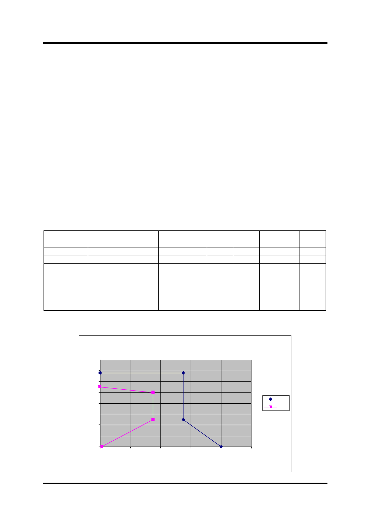
6.2.3 Output characteristics
Output caracteristics
8
7
6
5
4
3
Max
Min
2
1
0
0 200 400 600 800 1000
Output current [mA]
Page 2. 8
Technical Manual
Issue 1
November 2002

Input parameter Type Value Unit
Input voltage EU,UK, CH min 90 V
nom 230 V
max 253 V
Extended voltage range min 0 V
max 264 V
Input frequency min 47 Hz
nom 50 Hz
max 63 Hz
Input current max 50 mA
Efficiency min >45 %
Inrush current max 25 A
Inrush current time max 10 ms
Output parameter Type Value Unit
Output current- min 350 mA
(2,5-5V load) nom 450 mA
Vin>207VAC max 500 mA
Output voltage- min 5.5 V
(No load) nom 6,5 V
max 6,8 V
Output current 2,5-5V load min 250 mA
(Vin < 207VAC) max 500 mA
Rise time min 10 ms
max 15 ms
Over voltage max 0.5 V
max 3 ms
Noise:
Ripple voltage Rms >120Hz max 50 mV
Ripple voltage p-p >120Hz max 200 mV
MX-7930/31/32
Page 2. 9
Technical Manual
Issue 1
November 2002

MX-7930/31/32
6.3 Output peak current
When accompany the phone by a current-limited voltage source, the phone provides simple,
accurate charge and termination control for single-cell Li+ battery 4.2V.
When the battery approaches full charge, its instantaneous voltage reaches the BATT
regulation voltage and pulsed top-off begins.
Charging current is set by the current limit of the external supply; current is not regulated
by the phone.
The phone switches the current-limited source on and off; because of the internal impedance
the current can prevents high voltages transient.
Excessive current into the battery can cause errors in the termination process of the phone
(by raising the instantaneous battery voltage) and ma y trip the battery’s protection circuitry.
1N4001
V+
Charger
V-
Testing circuit for output peak current I peak max. 2Amp
6.4 System Connector.
• Pin 1 and 2 : GND
• Pin 3 and 4 : V_EXD
• I/F Connector Plug
PART NR: 1006-1022-720
1N4001
1N4001
0.22 Ohm
SCOPE
6.5 Mechanical details
The charger shall weigh less than 80g.
UK charger shall weigh less than 110g.
Page 2. 10
Technical Manual
Issue 1
November 2002

MX-7930/31/32
Output voltage [V]
7. AX-721 Car charger.
7.1 Temperature ranges.
Operating temperature range is –20 to + 60°C, where the charger shall fulfil all specifications.
In the temperature ranges -25 to -20 and +60 to +70 °C the charger can be operated for a
short period. It doesn’t need to fulfil all specifications in previous mentioned temperature
ranges. Storage temperature range for the charger is –40 to +85°C.
7.2 Weight.
The cigar charger weights, including output DC cable, 55g.
7.3 Electrical specification.
7.3.1 Output requirements
Symbol Parameter Condition Min Typ Max Unit
Iout Output current Vi=10.8V to 28V 400 450 550 mA
Vout Output voltage No load 5,5 6,5 6,8 V
Temp Operating temperature range - -20 - +60 °C
Ripple Output ripple Vin=10.8 to 28V - - 200 mVp-p
Frequency Output - - 150 KHZ
Ipeak Output peak current Vin=10.8 to 28V - - 2 A
7.3.2 Input requirements
Parameter Min. RMS Max. RMS Max. peak
Input voltage 10.8 VDC 28VDC 31V
7.3.3 Output current
8
7
6
5
4
3
2
1
0
0 100 200 300 400 500 600 700 800 900
Output current [mA]
Vmax
Vmin
Page 2. 11
Technical Manual
Issue 1
November 2002

MX-7930/31/32
7.4 Output peak current
When accompany the phone by a current-limited voltage source, the phone provides simple,
accurate charge and termination control for single-cell Li+ battery 4.2V.
When the battery approaches full charge, its instantaneous voltage reaches the BATT
regulation voltage and pulsed top-off begins.
Charging current is set by the current limit of the external supply; current is not regulated
by the phone.
The phone switches the current-limited source on and off; because of the internal impedance
the current can prevents high voltages transient.
Excessive current into the battery can cause errors in the termination process of the phone
(by raising the instantaneous battery voltage) and may trip the battery’s protection circu itry.
1N4001
V+
Charger
V-
Testing circuit for output peak current I peak max. 2Amp
7.5 System Connector.
• Pin 1 and 2 : GND
• Pin 3 and 4 : V_EXD
• I/F Connector Plug
PART NR: 1006-1022-720
1N4001
1N4001
0.22 Ohm
SCOPE
Page 2. 12
Technical Manual
Issue 1
November 2002

MX-7930/31/32
8. AX-772 Data/fax cable.
AX-772 consists of an RS-232 interface to a standard PC COM port, and an interface to MX7930/31/32 GSM phone.
The GSM phone power the interface. This is due to the reason that the throughput, when
using software flow control, is lower than when using hardware flow control.
8.1 Block diagram for AX-772
LDO
EXTIFEN
DTR
TX
RX
DCD
DSR
Ri
RS-232 interface
SG4500 phone interface
USC3 (CS_DCD)
ACC_DET
USC1 (Rx)
USC2 (Tx)
USC5 (RTS) CTS
USC4 (CTS) RTS
USC6 (Ri)
/CS
Buffer
GND
RS-232 converter
(Inverter and
level converter)
ID resistor
8.2 ACC_DET :
In order to enable the phone to detect the kind of accessory that is connected, each type of
accessory has it’s own ID-resistor. The data-fax cable has two ID-resistor values, one for
DTR low and one for DTR high. This will make it possible to read the DTR states and also
make it possible to detect when a data cable is connected to the phone. When DTR is low,
not connected to a pc, the ID-resistor must be 22k ohm and when DTR is high the ID-resistor
must be 13k ohm. See Figure 8-1
DTR line RS-232 level
R
R
ID1
R
ID2
ACC_DET
R
ID1
=22k 1%
=32k 1%
ID2
Figure 8-1 ID/DTR interface
Page 2. 13
Technical Manual
Issue 1
November 2002

MX-7930/31/32
8.3 Mechanical.
8.3.1 DB-9 plug.
The DB-9 plug must contain the DB-9 connector and the RS-232 converter circuit. The DB-9
connector must be a SUB D 9 way Female connector
The DB 9 way receptacle connectors must meet the "DeFacto" Standards requirements for
sub miniature D connectors used for input/output applications in the Computer and Business
Equipment Industries, and must conform to meet Office Class I Standards, DIN 41652 and
DIN 41620.
8.3.2 System plug
The system plug must conform the test specification for the system plug. The system plug for
the phone must be with a socket, so that makes it possible to attach a charger when using a
data/fax cable. The system socket must be the same as for the MX-7930/31/32. The actual
mechanical design is not fixed.
8.3.3 Cable Data:
Cable Length 150 cm
Cable diameter 5mm
Weight, max 50 g
Colour Black
Page 2. 14
Technical Manual
Issue 1
November 2002

8.3.4 Electrical Data
Power supply current max. 50mA
8.3.5 Phone interface:
, drawn from EXTIFEN
AVG
MX-7930/31/32
Pin
1 GND N/A
2 GND N/A
3 V_EXT See doc [1]
4 V_EXT See doc [1]
5 USC0 Not to be used
6 USC5 Low[0 – 0.2] High[2.5 – 2.82]
7 USC1 Low[0 – 0.72] High[1.75 – 3.0]
8 USC3 Low[0 – 0.2] High[2.5 – 2.82]
9 USC4 Low[0 – 0.72] High[1.75 – 3.0]
10 USC2 Low[0 – 0.2] High[2.5 – 2.82]
11 USC6 Low[0 – 0.2] High[2.5 – 2.82]
12 ACC_DET Analogue ID
13 EXTIFEN +3 to +5.5 Volt
14 JTAG0 Not to be used
15 JTAG1 Not to be used
16 JTAG2 Not to be used
17 JTAG3 Not to be used
18 JTAG5 Not to be used
19 GSPB-RX Not to be used
20 GSPB-TX Not to be used
21 VPP/ /SYS_RESET Not to be used
22 GND N/A
Signal Description
8.3.6 RS-232 interface:
Pin Signal Direction from AX-772
1 DCD Low[-5 – -15] High[5 – 15]
@ 3kΩ to 7 kΩ load
2 TX Low[-5 – -15] High[5 – 15]
@ 3kΩ to 7 kΩ load
3 Rx Low[-5 – -15] High[5 – 15]
@ 3kΩ to 7 kΩ load
4 DTR Low[-5 – -15] High[5 – 15]
@ 3kΩ to 7 kΩ load
5 GND N/A
6 DSR Low[-5 – -15] High[5 – 15]
@ 3kΩ to 7 kΩ load
7 RTS Low[-5 – -15] High[5 – 15]
@ 3kΩ to 7 kΩ load
8 CTS Low[-5 – -15] High[5 – 15]
@ 3kΩ to 7 kΩ load
9 RI Low[-5 – -15] High[5 – 15]
@ 3kΩ to 7 kΩ load
Page 2. 15
Technical Manual
Issue 1
November 2002

MX-7930/31/32
9. AX-773 USB cable.
The AX-773 is a cable with a MX-7930/31/32 system connector plug in one end, a small lump
on the cable near the system connector where the necessary electronics is placed, and finally
a USB up link connector at the other end of the cable. It plugs directly into a USB port on a PC
or a USB hub and into the MX-7930/31/32.
The AX-773 is powered by the PC USB port or USB hub port and is in high-power mode
(software controlled) able to charge the phone with 300 to 400mA. Alternatively the AX70x
(travel charger) or the AX-721 (car charger) can be used to charge the phone while using the
USB.
9.1 Diagram for AX-773
The circuit supports both low- and high-power bus. When connecting to a high-power bus it is
possible to charge the phone with 300 to 400 mA (software controlled). Figure 9-1 shows a
simple block diagram of the AX-773. Notice that the female system connector for charging the
phone while the USB cable is in use is not shown on the diagram.
EXTIFEN
CS
CLK
Sirius phone interface
TXD
IRQ
RXD
CHR_DET
USB_PWR_EN
ACC_DET
LDO
USB
USBN9603
National
Constant current
charger
ID resistor
GND
D
+
D
-
Figure 9-1: Simple block diagram of the AX-773.
USB interface
Page 2. 16
Technical Manual
Issue 1
November 2002

MX-7930/31/32
9.2 Electrical interface.
In order for the phone to detect the kind of accessory connected to the phone, each type of
accessory has an ID resistor. The ID resistor for AX-773 shall be 11.8kΩ 1%, according to the
specification for the MX-7930/31/32 phone.
When the phone has detected that an AX-773 cable attached, it will enable the supply to the
AX-773 cable (EXT_PWR_ON).The signal is only used for enable the LDO on the circuit and
not for power supply, which will be provided by the USB port.
9.2.1 Interface to PC
Pin # Signal Description Direction from
AX-771
1 VBUS Power from the USB port Input
2 D- USB D- upstream port Output
3 D+ USB D+ upstream port Input
4 GND GND N/A
Pin Signal Description
1 GND N/A
2 GND N/A
3 V_EXT See doc [1]
4 V_EXT See doc [1]
5 CLK Clock for USB data
6 CHR_DET Charger detected.
7 RxD Data from USB
8 \CS Chip enable of the USB cable.
9 USB_PWR_EN Enable of USB charger.
10 TxD Data to USB
11 IRQ Interrupt from USB cable.
12 ACC_DET Analogue ID
13 EXTIFEN +3 to +5.5 Volt
14 JTAG0 Not to be used
15 JTAG1 Not to be used
16 JTAG2 Not to be used
17 JTAG3 Not to be used
18 JTAG5 Not to be used
19 GSPB-RX Not to be used
20 GSPB-TX Not to be used
21 VPP/ /SYS_RESET Not to be used
22 GND N/A
Page 2. 17
Technical Manual
Issue 1
November 2002

MX-7930/31/32
9.3 Summary
Table 9-1 is only meant as an overview of some of the requirements for the AX-773.
Physical requirements of the AX-771
Length
Diameter TBD
Weight, max TBD
Colour Mat black
Temperature range
Operating 0°C to +50°C
Storage -20°C to +60°C
Norminal +20°C
Cable characteristics
Differential characteristic impedance Z0 = 90Ω ± 15%
Common mode cable impedance Z
Cable delay 5.2 ns/m and total max 26 ns
Cable skew 100 ps
Cable loss Refer to section 9.3.1
Table 9-1: Requirements for the AX-773.
The maximum allowable cable length is determined
by signal pair attenuation and propagation delay.
= 30Ω ± 30%
CM
9.3.1 Cable delay
The maximum total one-way signal propagation delay allowed is 30 ns. The allocation for
cable delay is 26 ns. A maximum delay of 3 ns is allowed from a Host or Hub Controller
downstream facing transceiver to its exterior downstream facing connector, while a maximum
delay of 1 ns is allowed from the upstream facing connector to the upstream facing
transceiver of any device. For a standard USB detachable cable, the cable delay is measured
from the Series A connector pins to the Series B connector pins and is no more than 26 ns.
For other cables, the delay is measured from the series A connector to the point where the
cable is connected to the device – in this case the USB print. The cable delay must also be
less than 5.2 ns per meter.
The maximum one-way data delay on a full-speed cable is measured as shown in Figure 9-2.
Host/Hub .
Downstream
port
3ns (max) 1ns (max)
A-connector Host/Hub System-connector Sirius
A-connector System-connector
USB
print
Total one-way propagation delay
30ns (max)
One-way cable delay
26ns (max)
5.2ns/m (max)
Sirius
phone
Figure 9-2: Measurement of full-speed cable delay.
Page 2. 18
Technical Manual
Issue 1
November 2002

MX-7930/31/32
10. Battery- pack 550mAh
10.1 Electrical specification.
No. Item Specification
1 Charge Voltage 4.2 +/- 0.05V
2 Charge current Max: 1C
3 Discharge current Max: 2C
4 Capacity (1C) > 550mAh
6 Output Voltage Nominal: 3.7V
7 Z: out Incl. Protection circuit Max: 150mΩ
8 Cycle life Min: 300 th
9 Charging Current Std. 550mA
10 Charging Time 2.5hrs.
11 Charging Method Constant Current – Constant Voltage
10.2 Temperature:
For Chagrin: 0 - + 45°C
For Discharge: - 20 - + 60°C
10.3 Storage Temperature:
Within 1 month: - 20 - + 45°C
Within 6 month: - 20 - + 35°C
10.4 Applicable documents
The battery package is keeping the mentioned generic standards regarding CE marking IEC
950, and the (EU) Battery Directive (91/157/EEC, as amended by 93/86/EEC). External
connections
BATT_GND
BATT_POS
BATT_POS: The connecter is direct connected to the battery cell, and shall be used for
charge and discharge.
GND: Ground.
Page 2. 19
Technical Manual
November 2002
Issue 1

MX-7930/31/32
10.5 Protection circuit
10.5.1 Feature Description
The function of the IC protects the Li-Ion/Polymer Battery from damage due to overcharge,
over discharge, over current and short circuit conditions by disconnecting it from the load or
the charger. The control circuitry as well as the low resistive FET switch is integrated on
the same die. A more detailed description of the features of the chip is given in the following
paragraphs.
10.5.2 Overcharge Voltage Protection
If the battery voltage exceeds V ch+ the battery is disconnected from the charger after the
output delay of overcharge t vch+. If the battery voltage drops below V ch+ again during t vch+
nothing happens. The overcharge state is reset either if the battery voltage drops below V ch+
- ?V ch or if the charger is disconnected when the battery voltage is between V ch+ and V ch+ ?V ch. If the chip is in overcharge state and the battery voltage is above V ch+ the discharge of
the battery is possible with a voltage drop of about 1 V in the chip. In the overcharge state
where the battery is disconnected from the charger the charger voltage is not allowed to
exceed the maximum input voltage V max .If V max is exceeded there is no guarantee about
the status of the chip and the battery.
10.5.3 Over discharge Voltage Protection
If the battery voltage drops below V di the battery is disconnected from the load after the
output delay of over discharge t vdi. If the battery voltage exceeds V di again during t vdi
nothing happens.
The over discharge state is only reset if a charger is connected and the battery voltage is
above V di Even if the over discharge protection is activated the charging of the battery is
possible with a voltage drops of about 1 V in the chip. If an over discharge condition is
detected the device will enter a low current mode where only the charger detector is running.
10.5.4 Overcharge Current Protection
If the charger current exceeds I occ the battery is disconnected from the charger after the
overcharge current delay time t Iocc. If the current drops again below I occ during t Iocc
nothing happens. This state is reset if the charger is disconnected from the battery.
10.5.5 Over discharge Current Protection
If the discharge current exceeds I odc the battery is disconnected from the load after the
Over discharge current delay time t Iodc. If the current drops again below I odc during t Iodc
nothing happens. The over discharge current state is reset when the load is disconnected. To
sense the load a pull down is connected to the output. The leakage current due to this pull
down is smaller than I lodc.
10.5.6 Short Circuit Protection
If the voltage across the on resistance of the switching element exceeds the short protection
voltage V Short the battery is disconnected from the load. The maximum delay time to switch
the current off is t sc. This state is reset by disconnecting the load. To sense the load a pull
down is connected to the output. The leakage current due to this pull down is smaller than I
lodc.
10.5.7 Current Consumption
When the battery voltage is above V di the IC is working in normal mode where all the circuitry
is active. In this mode the mean current consumption is I n. If an over discharge condition is
present the device goes into a low power mode where only the power on reset and the polarity
or charger detector are active. The mean current consumption in this mode is I lp. The low
power mode is resetif a charger is connected.
Page 2. 20
Technical Manual
Issue 1
November 2002

MX-7930/31/32
11. Battery- pack 900mAh
11.1 Electrical specification.
No. Item Specification
1 Charge Voltage 4.2 +/- 0.05V
2 Charge current Max: 1C
3 Discharge current Max: 2C
4 Capacity (1C) > 900mAh
6 Output Voltage Nominal: 3.7V
7 Z: out Incl. Protection circuit Max: 150mΩ
8 Cycle life Min: 300 th
9 Charging Current Std. 550mA
10 Charging Time 4 hrs.
11 Charging Method Constant Current – Constant Voltage
11.2 Temperature:
For Chagrin: 0 - + 45°C
For Discharge: - 20 - + 60°C
11.3 Storage Temperature:
Within 1 month: - 20 - + 45°C
Within 6 month: - 20 - + 35°C
11.4 Applicable documents
The battery package is keeping the mentioned generic standards regarding CE marking IEC
950, and the (EU) Battery Directive (91/157/EEC, as amended by 93/86/EEC). External
connections
BATT_GND
BATT_POS
BATT_POS: The connecter is direct connected to the battery cell, and shall be used for
charge and discharge.
GND: Ground.
Page 2. 21
Technical Manual
November 2002
Issue 1

MX-7930/31/32
11.5 Protection circuit
11.5.1 Feature Description
The function of the IC protects the Li-Ion/Polymer Battery from damage due to overcharge,
over discharge, over current and short circuit conditions by disconnecting it from the load or
the charger. The control circuitry as well as the low resistive FET switch is integrated on the
same die. A more detailed description of the features of the chip is given in the following
paragraphs.
11.5.2 Overcharge Voltage Protection
If the battery voltage exceeds V ch+ the battery is disconnected from the charger after the
output delay of overcharge t vch+. If the battery voltage drops below V ch+ again during t vch+
nothing happens. The overcharge state is reset either if the battery voltage drops below V ch+
- ?V ch or if the charger is disconnected when the battery voltage is between V ch+ and V ch+ ?V ch. If the chip is in overcharge state and the battery voltage is above V ch+ the discharge of
the battery is possible with a voltage drop of about 1 V in the chip. In the overcharge state
where the battery is disconnect ed from the charger the charger voltage is not allowed to
exceed the maximum input voltage V max .If V max is exceeded there is no guarantee about
the status of the chip and the battery.
11.5.3 Over discharge Voltage Protection
If the battery voltage drops below V di the battery is disconnected from the load after the
output delay of over discharge t vdi. If the battery voltage exceeds V di again during t vdi
nothing happens. The over discharge state is only reset if a charger is connected and the
battery voltage is above V di Even if the over discharge protection is activated the charging of
the battery is possible with a voltage drops of about 1 V in the chip. If an over discharge
condition is detected the device will enter a low current mode where only the charger detector
is running.
11.5.4 Overcharge Current Protection
If the charger current exceeds I occ the battery is disconnected from the charger after the
overcharge current delay time t Iocc. If the current drops again below I occ during t Iocc
nothing happens. This state is reset if the charger is disconnected from the battery.
11.5.5 Over discharge Current Protection
If the discharge current exceeds I odc the battery is disconnected from the load after the over
discharge current delay time t Iodc. If the current drops again below I odc during t Iodc nothing
happens. The overdischarge current state is reset when the load is disconnected. To sense
the load a pull down is connected to the output. The leakage current due to this pull down is
smaller than I lodc.
11.5.6 Short Circuit Protection
If the voltage across the on resistance of the switching element exceeds the short protection
voltage V Short the battery is disconnected from the load. The maximum delay time to switch
the current off is t sc . This state is reset by disconnecting the load. To sense the load a pull
down is connected to the output. The leakage current due to this pull down is smaller than I
lodc.
11.5.7 Current Consumption
When the battery voltage is above V di the IC is working in normal mode where all the circuitry
is active. In this mode the mean current consumption is I n. If an overdischarge condition is
present the device goes into a low power mode where only the power on reset and the polarity
or charger detector are active. The mean current consumption in this mode is I lp. The low
power mode is resetif a charger is connected.
Page 2. 22
Technical Manual
Issue 1
November 2002

MX-7930/31/32
12. Portable hands free AX-790
This section describes all acoustic and electrical requirements for the headset.
12.1 Earphone
Earphone type: In ear type, mono dynamic
Drive unit: 15mm with ferrite magnet
Impedance: 32 ohm ± 4 ohm
Frequency
response: See Fig. 1.
Cord length: 1.5 meters shielded cable
S.P.L.: 108 ± 3 dB (1 mW)
Nominal input
power: 1mW
Maximum input
Power: 25mW
Earphone characteristic
20
10
0
-10
Level [dB]
-20
-30
-40
100 1000 10000
Max
Min
Typ
Fig. 1. Relative dB scale
Freq [Hz]
Page 2. 23
Technical Manual
Issue 1
November 2002

MX-7930/31/32
12.2 Microphone
Microphone type: Condenser Microphone
Sensitivity: -48 ± 3 dB at 1kHz (0dB = 1V/Pa) Vcc = 2 Volt. RL = 2.2 kohm
Frequency
response: See Fig. 2.
Capacitor: 10pF and 33pF SMD type between Mic+ and Mic- or internally
mounted inside the microphone.
Button: A button that short/mute the microphone
Microphone characteristic
10
5
0
-5
-10
-15
Level [dB]
-20
-25
-30
-35
-40
100 1000 10000
Freq [Hz]
Relative dB scale
Max
Min
Typ
Fig. 2.
Page 2. 24
Technical Manual
Issue 1
November 2002

Cable
: Cord length is 1.5 meter long
: 170 mm ± 10mm wire between microphone and Earphone.
: Is fitted with a little cloth peg under the microphone
: The microphones cord is shielded
Connector
Type : 2,5mm jack plug with 90 deg. angle (4 pole).
Connections
MX-7930/31/32
1 2 3
Microphone : Mic+ to pin 3 and Mic- to pin 4
Earphone : Ear to pin 1 and 2
Print
Earphone : Maxon
Microphone : Maxon
4
Page 2. 25
Technical Manual
Issue 1
November 2002

13. Terms and abbreviations
MX-7930/31/32
Term and
Abbreviation
FS Frame Sync
GPS Global Positioning System
IrDA Infrared Data Association
MC Memory Card. Either SD memory card or MMC
MMC MultiMediaCard
SD Memory Card Secure Digital Memory Card
ADC Analog to Digital Converter
ADI Analog Devices, Inc.
MP Mass Production
TBD To Be Defined or To Be Determine.
UART Universal Asynchronous Receiver Transmitter
USART Universal Synchronous Asynchronous Receiver Transmitter
Description
Table 13-1: Table of terms and abbreviations.
Page 2. 26
Technical Manual
Issue 1
November 2002
 Loading...