

Page 1
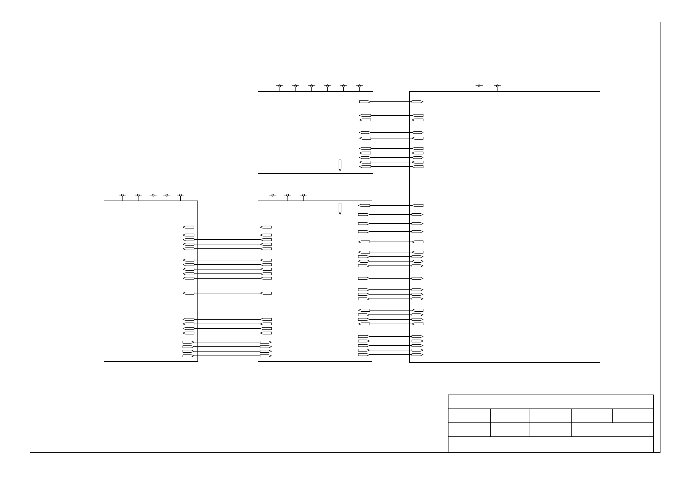
N
F
N
2
R
FVRF
C
A
r
K
N
C
A
N
N
A
R
VPW
VCCDVBAT VTI
VUH
VBAT
VCCD
SIM and Power
Management
(5)
TAPRESNT
LAM
PWRON0
SRLDATA
SRLCLK
BOOSTE
SIME
SIMDATA
SIMCLK
SIMRST
VUHF VBAT
VRF VTIC VCCD VBAT VPWRVCCD
PACOUT
TXEN1
RXEN1
Radio
Interface
Block
(2)
SYNDAT
SYNLE
SYNCLK
SYNE
TXEN0
SYNRE
VC4
VC1
Baseband
udio Interface
(3)
TXIP
TXI
TXQP
TXQN
RXIP
RXIN
RXQP
RXQN
PO
PCONT
RESETB
FRT
HDSTDET
BPDET
CTLRT
CTLCLK
CTLDATA
RPNSDAT
SYSCLK
RXCL
RXDAT
RXRT
CDCCLK
CDCRT
ENCDATA
DECDATA
VCONT
SDI
SYN
SCLK
IRQ
GSM Processo
(4)
Title
MX-5010 System Block Diagram
System
MX-5010
FCC ID
AWWMX5010
PROPRIETARY INFORMATION
Any part of this document must not be disclosed to third parties without prior written permission.
HW Rev.
2.50
Date
2002/05/08
Drawn by
K.Tsuchida
Page
1 of 5
Chk’d by
S.Ohmomo
Approved by
K.Sakayori
Maxon Telecom Co., Ltd.
Page 2
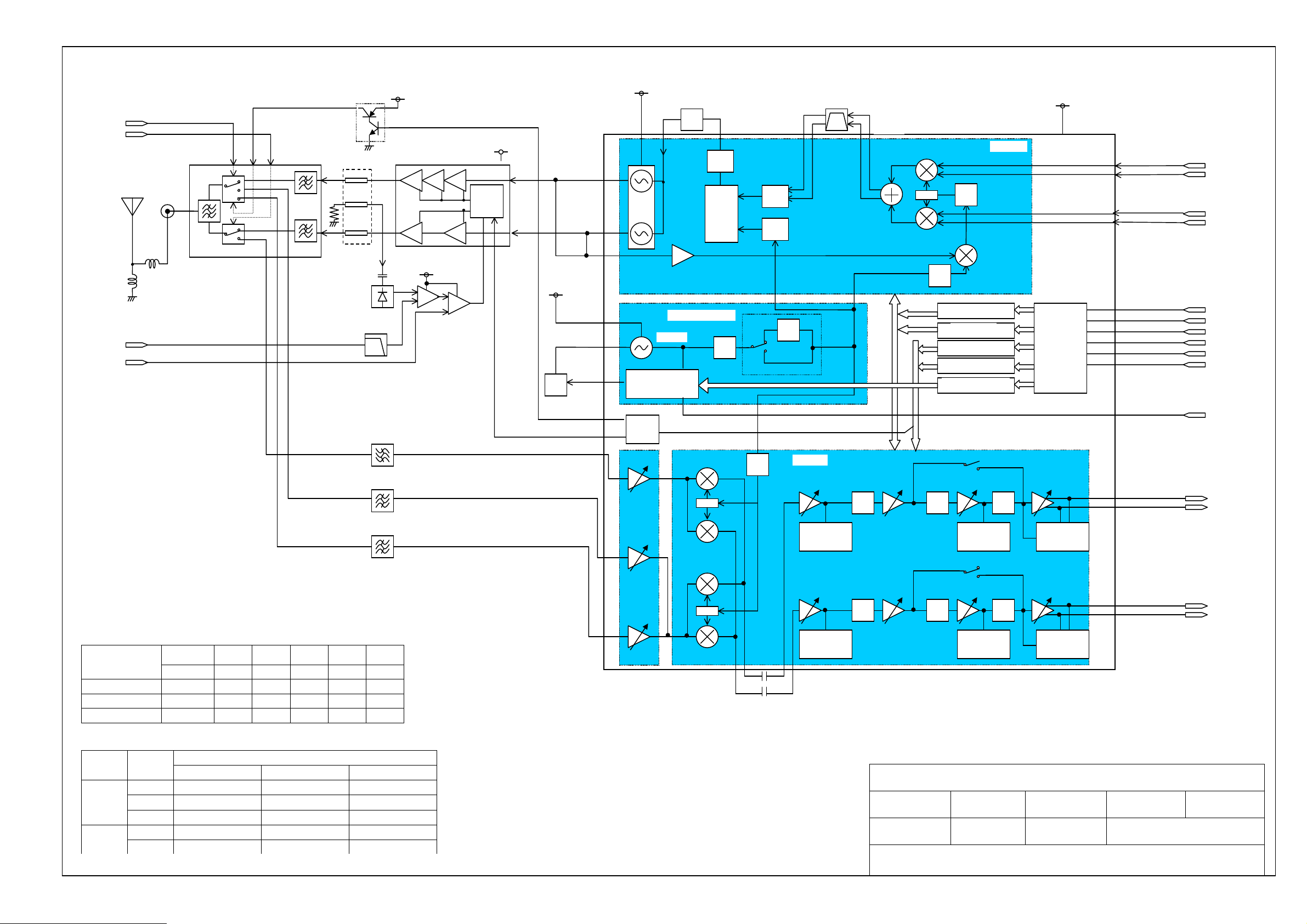
N
N
E
A
r
A
2
2
A
l
A
CONT
VC1
VC4
IC101
T/R SW
F_tx
Q101
VRF
IC201 PA CX77304
MP101
NTENNA
P101
RF
Connecto
F_tx
F201
Coupler
D201
RF Detector
VTIC
PACOUT2
TXEN0
PACOUT2
F_rx
F101
GSM Rx SAW
[ARFCN Allocation]
EGSM: 975-1023, 0-124
DCS: 512-885
PCS: 512-810
[Frequency Calculation]
F_Tx = K/3 * (2-D2/D1) * F_lo
F_Rx = 2 / 3 * F_lo
(EGSM band)
F_Rx = 4 / 3 * F_lo
(DCS/PCS band)
F102
DCS Rx SAW
F103
PCS Rx SAW
Table A. T/R Switch Control
Symbol EGSM DCS PCS
Tx Rx Tx Rx Tx Rx
VC1Mo L L H L H L
CONT2 L L L L L H
VC4 H L L L L L
Table B. Frequency Plan
Mode Symbol Frequency Plan [MHz]
EGSM DCS PCS
Transmit F_Tx 880.2 - 914.8 1710.2 - 1784.8 1850.2 - 1909.8
F_lo 1473.0 - 1543.7 1344.0 - 1414.5 1449.7 - 1516.6
F_tx_if 90.5 - 114.4 74.8 - 104.8 80.5 - 112.3
Receive F_Rx 925.2 - 959.8 1805.2 - 1879.8 1930.2 - 1989.8
F lo 1387.8 - 1439.7 1359.9 - 1409.9 1447.7 - 1492.4
IC203
PAC AMP
-
+
VRF
F_tx_if
K
X2
TXIFP
TXIFN
D2
D1
X2
Rx Path
DC offset
Canceller
DC offset
Canceller
LPF
V-BAT
TXDCS/PCS
PC /
Band
Sel.
TXGSM
TXINP
-
+
VUHF
LPF
PCO
PCO1
Fractional-N
PLL
Band
Select
TXVCO
TUNE
Sx (Synthesizer)
F_lo
ux Contro
TXCPO
CP
PFD
1/3
PSN
PSN
FILTP
FILTN
Tx Path
LPF
PSN
LPF LPF LPF
LPF LPF LPF
LPF
X2
Rx/Tx Control
ux Control
IP2 Calibration
DC Offset Timing
Sx Register 1/2
DC offset
Canceller
LPF
DC offset
Canceller
VCCD
Control
Registers
DC offset
Canceller
DC offset
Canceller
TXIP
TXI
TXQP
TXQ
SYNDAT
SYNL
SYNCLK
SYNEN
TXEN1
RXEN1
SYNREF
RXIP
RXIN
RXQP
RXQN
IC301 DCR CX74017
Title
Radio Interface Block Diagram
System
MX-5010
FCC ID
AWWMX5010
PROPRIETARY INFORMATION
Any part of this document must not be disclosed to third parties without prior written permission.
HW Rev.
2.50
Date
2002/05/08
Drawn by
K.Tsuchida
Page
2 of 5
Chk’d by
S.Ohmomo
Approved by
K.Sakayori
Maxon Telecom Co., Ltd.
Page 3

Rx D
g
(R
K
A
r
r
E
r
r
Σ∆
r
Σ∆
r
Σ∆
r
Σ∆
A
R
T
Tx Digital A
Rx Digital Audi
3.9
r
g
A
A
A
C
A
r
S
GS
S
R
S
Power Ramp
Control
ynthesizer / DCR
Control
Timing
ynth. Reference
19.5MHz
Receive
I / Q Signals
Melody IC
Control
PCON
Transmit
I / Q Signals
PACOUT2
SYNDAT
SYNL
SYNCLK
SYNEN
TXEN0
Tx / Rx
Control
TXEN1
VC1
VC4
RXEN1
M Frame
SYNREF
HDSTDET
IC704
VDD Reg.
VCONT
SDIN
SYN
SCLK
IRQ
RESETB CR
R417, R418
C447
TXIP
TXIN
TXQP
TXQN
FRT
BPDET
RXIP
RXIN
RXQP
RXQN
V-C10
VCCD
VPW
V-C10
LDO Regulators
Bandgap
Q705
Q704
Internal supplies
LPF
LPF
10bit DAC
10bit DAC
RAMP DAC
IC401 Integrated Analog Processo
CX20505
Internal ref.
Bias generator
Voltage
generato
Offset
Phase / Gain
Balance
16-Bit
32 x16-Bit
Ramp Store
Reset
Logic
GMSK
Modulato
148-bits
Burst Store
ystem Reset
PO
RESETB
Tx Data and
VBAT
V.Re
Serial I/F
FIFO
32 words
Reset
.
(AVDD)
Score
Data
R419, C410, C411, L401
eceive I / Q Signal)
MP401
MIC
P401
Headset Jack
MP402
EP receiver
VCCD
Timbre Data
Tempo
Start/Stop
Timbre
llotment
Sequencer
Trap
UXIN
UXOUT
HDSTDET
Timbre
Register
FM
Synthesizer
MIC+
MIC-
Bias
Bias
IC402
Melody IC YMU757B
DAC &
Volume
GPO
Mapping
Logic
ADC
LPF
LPF
LPF
MP403
udio Speake
Temp.
Senso
8-Bit
Aux-ADC
Decimator
DecimatorADC
ADC
DAC
Tune Store
Intra-Frame
Sequencer
Status &
Monito
Clock
Gen
FIR
Filte
FIR
Filte
FIR
Filter
FIR
Filte
Control
Serial
Interface
CCXO
Tune
Receiver
Serial
Interface
CODEC
Serial
Interface
Title
Baseband / Audio Interface Block Diagram
System
MX-5010
FCC ID
AWWMX5010
PROPRIETARY INFORMATION
Any part of this document must not be disclosed to third parties without prior written permission.
Radio Control I/O
F401
19.5MHz
X’tal
MHz Master Clock
ata to Baseband
Di
ital Audio Data
HW Rev.
2.50
Date
2002/05/08
udio
o
Drawn by
K.Tsuchida
Page
3 of 5
CTLRT
CTLCLK
CTLDATA
RPNSDAT
SYSCLK
RXCL
RXDAT
RXRT
CDCCLK
CDCRT
ENCDA
DECDA
Chk’d by
S.Ohmomo
Approved by
K.Sakayori
Maxon Telecom Co., Ltd.
Page 4

IC601 B
CX80
A
r
K
A
N
C
N
N
r
A
A
GSM F
g
C
P
l
A
Vib
SIM I/O
P
l
S
3.9
SYSCLK
MHz Master Clock
CLKRQST
aseband Processor
RESETB
IC702 (1/2)
ND
VCCD
F_RP
(Flash Reset)
ARM
Interrupt
Controller
Clock
enables
IC602
FLASH/SRAM
FLASH ROM
8MB (x8bits)
SRAM
1MB (x8bits)
External
Bus
CRC
Timers
DMA
Controller
VBAT
CTLRT
CTLCLK
CTLDATA
RPNSDAT
RXCL
RXDAT
RXRT
CDCCLK
CDCRT
ENCDATA
DECDATA
Control
Port
Receive
Port
CODEC
Port
IC706
DC/DC Conv.
LM2750.
DC/DC
LEDCTL
VBAT
Backlight
LEDs
VCCD
H801
LCD
5
Clock Generation
and PLL
IROM CACHE
IRAM
Internal
Core
Supply
RM7 Thumb
CPU Core
Layer2/3 Processing
MMI/Browser etc.
Dual-port RAM
DSP Core
CODEC
Ciphering Layer1
Keypad
/LCD
I/F
ViterbiSpeech
P501
BtoB
Connecto
LDO
32kHz
RTC
System
Reset
Serial
Bus
IrDA
Pulse
Shape
Escape
Sequence
/Flow
Control
Serial
Port
(SDS)
Debug
Port
(DBG)
Auto
Baud
GPIO
SIM I/F
F601
RTC
X’tal
32kHz
BT701
Backup Battery
DAIRST / HDSTDET
SEND
END
(POWER)
Reg.
IC703
RTC Reg.
IRDAEN
VBAT VCCD
IC603
IrDA Module
SDSTX
SDSRX
DAITX
DAIRX
DAIRST
DAICLK
LAM
RESETB
SRLDATA
SRLCLK
PJ601 (1/2)
System Connector
VCONT
SDI
SYN
SCLK
IRQ
FRT
PCONT
TAPRESNT
ESES
MEN
BOOSTE
SIME
SIMDATA
SIMCLK
SIMRST
ower Contro
ystem Reset
Power
Management
Block Control
Melody I
Control
rameTimin
ower Contro
ccessory Detect /
Power Control
rating Alert
MMI
PCB
1
4
7
9
*
2
5
8
0
3
6
#
Q802
PWRON0
Title
GSM Processor Block Diagram
System
MX-5010
FCC ID
AWWMX5010
PROPRIETARY INFORMATION
Any part of this document must not be disclosed to third parties without prior written permission.
HW Rev.
2.50
Date
2002/05/08
Drawn by
K.Tsuchida
Page
4 of 5
Chk’d by
S.Ohmomo
Maxon Telecom Co., Ltd.
Approved by
K.Sakayori
Page 5

-
N
A
F
F
C
C
r
r
A
N
N
r
VCHRG
V-BAT
P701
Battery
Contact
+
ID
VBAT
BPDET
LAM
PWRON0
VCHRG
PJ601 (2/2)
System
Connecto
VCHRG1/2
EXTPWRSW
EXPWROUT
PMICRST
SRLDATA
SRLCLK
EXPWROUT
IC702 (2/2)
ND
PMICINT
SHUTDOWN
SYNEN
TXEN1
RXEN1
TAPRESNT
POR
BOOSTE
SIME
SIMDATA
SIMCLK
SIMRST
D703 Q701 R704
Charger
Control
Current
Sens
Amp
ontrol
Logic
Power
On
Reset
Reference
IC701
Power Management IC
CX20460
LDO Reg.
For
Digital
LDO Reg.
For
UHF VCO
LDO Reg.
For
RF circuit
LDO Reg.
For
Tx circuit
LDO Reg.
V3
Regulator
V7
Reg.
V8
SIM card
Regulator
SIM Card
Interface
VCCD
VUH
VR
VTI
Q702
External
Booste
P601
SIM Contact
VBAT
ESES
ME
VBAT
IC705
Regulator
VIN
OUT
ON
Q601
D603
D604
EXPWROUT
MP801
Vibrating
V
Moto
Title
SIM and Power Management Block Diagram
System
MX-5010
FCC ID
AWWMX5010
PROPRIETARY INFORMATION
Any part of this document must not be disclosed to third parties without prior written permission.
HW Rev.
2.50
Date
2002/05/08
Drawn by
K.Tsuchida
Page
5 of 5
Chk’d by
S.Ohmomo
Maxon Telecom Co., Ltd.
SIM
Approved by
K.Sakayori
 Loading...