

Page 1
xr XR16C2850
2.97V TO 5.5V DUAL UART WITH 128-BYTE FIFOS
NOVEMBER 2005 REV. 2.1.3
GENERAL DESCRIPTION
The XR16C28501 (2850) is an enhanced dual
universal asynchronous receiver and transmitter
(UART). Enhanced features include 128 bytes of TX
and RX FIFOs, programmable TX and RX FIFO
trigger level, FIFO level counters, automatic (RTS/
CTS) hardware and (Xon/Xoff) software flow control,
automatic RS-485 half duplex direction control output
and data rates up to 6.25 Mbps at 5V and 8X
sampling clock. Onboard status registers provide the user
with operational status and data error flags. An internal
loopback capability allows system diagnostics. The 2850
has a full modem interface and can operate at 2.97V
to 5.5V and is pin-to-pin compatible to Exar’s
ST16C2550 and XR16C2750 except the 48-TQFP
package. The 2850 register set is compatible to the
industry standard ST16C2550 and is available in 48pin TQFP and 44-pin PLCC packages.
NOTE: 1 Covered by U.S. Patent #5,649,122 and #5,949,787
APPLICATIONS
• Portable Appliances
• Telecommunication Network Routers
• Ethernet Network Routers
• Cellular Data Devices
• Factory Automation and Process Controls
FEATURES
Added feature in devices with a top mark date code of
"F2 YYWW" and newer:
■ 5V tolerant inputs
■ 0 ns address hold time (T
AH
)
• Pin-to-pin compatible and functionally compatible to
Exar’s ST16C2550 and XR16L2750 and TI’s
TL16C752B in the 48-TQFP package
• Pin-alike Exar’s XR16L2750 and ST16C2550 48-
TQFP package but with additional CLK8/16,
CLKSEL and HDCNTL inputs
• Two independent UART channels
■ Register set compatible to 16C550
■ Up to 6.25 Mbps at 5V, and 4 Mbps at 3.3V
■ Transmit and Receive FIFOs of 128 bytes
■ Programmable TX and RX FIFO Trigger Levels
■ Transmit and Receive FIFO Level Counters
■ Automatic Hardware (RTS/CTS) Flow Control
■ Selectable Auto RTS Flow Control Hysteresis
■ Automatic Software (Xon/Xoff) Flow Control
■ Auto RS-485 Half-duplex Direction Control
■ Wireless Infrared (IrDA 1.0) Encoder/Decoder
■ Full modem interface
• Device Identification and Revision
• Crystal oscillator or external clock input
• Industrial and commercial temperature ranges
• 48-TQFP and 44-PLCC packages
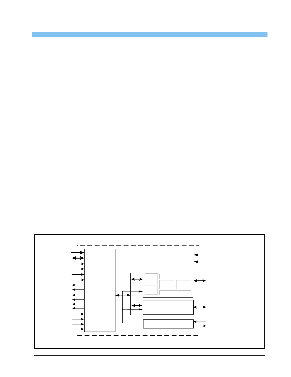
FIGURE 1. XR16C2850 BLOCK DIAGRAM
A2:A0
D7:D0
IOR#
IOW#
CSA#
CSB#
INTA
INTB
TXRDYA#
TXRDYB#
RXRDYA#
RXRDYB#
HDCNTL#
CLKSEL
CLK8/16
Reset
8-bit Data
Bus
Interface
UART Channel A
128 Byte TX FIFO
UART
Regs
TX & RX
BRG
128 Byte RX FIFO
UART Channel B
(same as Channel A)
Crystal Osc/Buffer
IR
ENDEC
2.97V to 5.5V VCC
GND
TXA, RXA, DTRA#,
DSRA#, RTSA#,
DTSA#, CDA#, RIA#,
OP2A#
TXB, RXB, DTRB#,
DSRB#, RTSB#,
CTSB#, CDB#, RIB#,
OP2B#
XTAL1
XTAL2
Exar Corporation 48720 Kato Road, Fremont CA, 94538 • (510) 668-7000 • FAX (510) 668-7017 • www.exar.com
Page 2
XR16C2850 xr
2.97V TO 5.5V DUAL UART WITH 128-BYTE FIFOS REV. 2.1.3
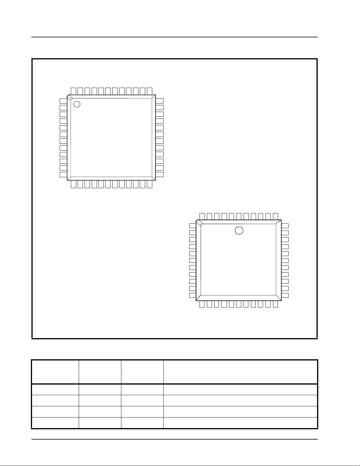
FIGURE 2. PIN OUT ASSIGNMENT
CDA#
DSRA#
RIA#
CTSA#
HDCNTL#
40
38
37
39
RESET
36
DTRB#
35
DTRA#
34
RTSA#
33
OP2A#
32
RXRDYA#
31
INTA
30
INTB
29
A0
28
A1
27
A2
26
CLKSEL
25
23
24
D5
D6
D7
RXB
RXA
TXRDYB#
TXA
TXB
OP2B#
CSA#
CSB#
D4
D3
D2D1D0
48
47
464544
1
2
3
4
5
6
7
8
9
10
11
12
NC
15
13
14
TXRDYA#
434241
XR16C2850
48-pin TQFP
1819202122
16
17
VCC
GND
IOW#
CDB#
XTAL2
XTAL1
ORDERING INFORMATION
PART NUMBER PACKAGE
RIB#
IOR#
RXRDYB#
DSRB#
RTSB#
CTSB#
CLK8/16
RXB
RXA
TXRDYB#
TXA
TXB
OP2B#
CSA#
CSB#
D4D3D2D1D0
6
5
4
7
D5
D6
8
D7
9
10
11
12
13
14
15
16
17
1819202122232425262728
IOW#
XTAL1
XTAL2
TXRDYA#
3
2
1
XR16C2850
44-pin PLCC
GND
CDB#
RXRDYB#
VCC
RIA#
CDA#
DSRA#
4443424140
RIB#
IOR#
RTSB#
DSRB#
CTSA#
RESET
39
DTRB#
38
DTRA#
37
RTSA#
36
OP2A#
35
RXRDYA#
34
INTA
33
INTB
32
A0
31
A1
30
A2
29
CTSB#
OPERATING
EMPERATURE
T
ANGE
R
DEVICE STATUS
XR16C2850CJ 44-Lead PLCC 0°C to +70°C Active
XR16C2850CM 48-Lead TQFP 0°C to +70°C Active
XR16C2850IJ 44-Lead PLCC -40°C to +85°C Active
XR16C2850IM 48-Lead TQFP -40°C to +85°C Active
2
Page 3
xr XR16C2850
REV. 2.1.3 2.97V TO 5.5V DUAL UART WITH 128-BYTE FIFOS
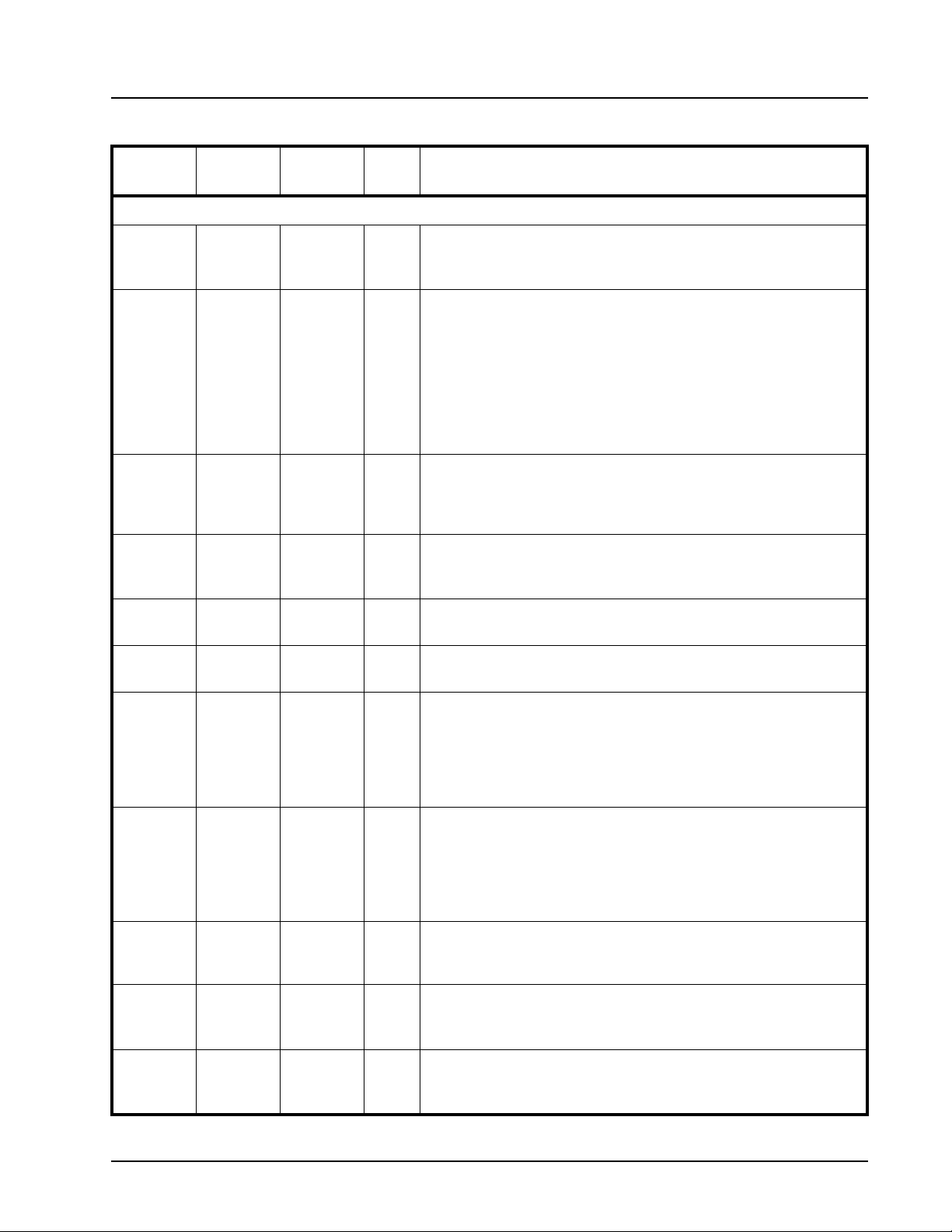
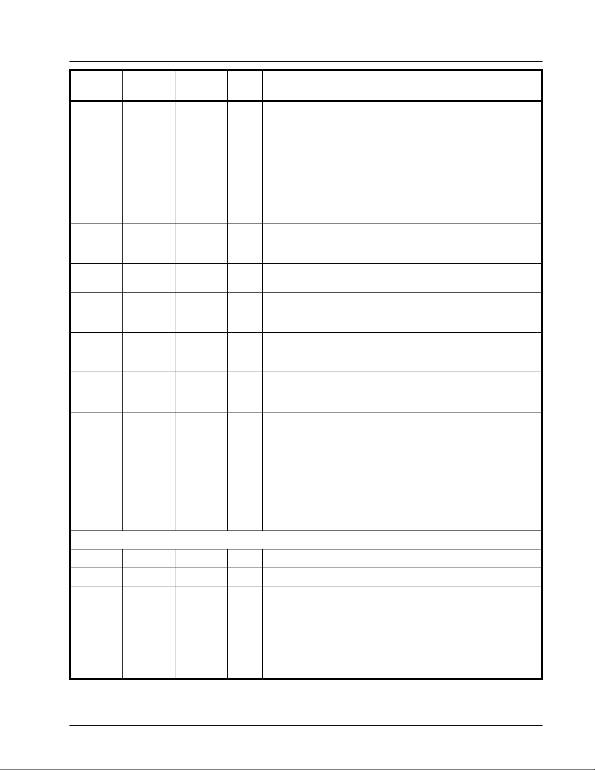
PIN DESCRIPTIONS
NAME
DATA BUS INTERFACE
A2
A1
A0
D7
D6
D5
D4
D3
D2
D1
D0
IOR# 24 19 I
IOW# 20 15 I
CSA# 16 10 I
44-PLCC
PIN #
29
30
31
9
8
7
6
5
4
3
2
48-TQFP
PIN #
26
27
28
3
2
1
48
47
46
45
44
TYPE DESCRIPTION
I
Address data lines [2:0]. These 3 address lines select one of the internal registers in UART channel A/B during a data bus transaction.
I/O
Data bus lines [7:0] (bidirectional).
Input/Output Read Strobe (active low). The falling edge instigates an
internal read cycle and retrieves the data byte from an internal register
pointed to by the address lines [A2:A0]. The data byte is placed on the
data bus to allow the host processor to read it on the rising edge.
Input/Output Write Strobe (active low). The falling edge instigates an
internal write cycle and the rising edge transfers the data byte on the
data bus to an internal register pointed by the address lines.
UART channel A select (active low) to enable UART channel A in the
device for data bus operation.
CSB# 17 11 I
INTA 33 30 O
INTB 32 29 O
TXRDYA# 1 43 O
RXRDYA# 34 31 O
TXRDYB# 12 6 O
UART channel B select (active low) to enable UART channel B in the
device for data bus operation.
UART channel A Interrupt output. The output state is defined by the
user through the software setting of MCR[3]. INTA is set to the active
mode and OP2A# output is LOW when MCR[3] is set to a logic 1. INTA
is set to the three state mode and OP2A# is HIGH when MCR[3] is set
to a logic 0 (default). See MCR[3]. If this output is not used, leave it
unconnected.
UART channel B Interrupt output. The output state is defined by the
user through the software setting of MCR[3]. INTB is set to the active
mode and OP2B# output is LOW when MCR[3] is set to a logic 1. INTB
is set to the three state mode and OP2B# is HIGH when MCR[3] is set
to a logic 0 (default). See MCR[3]. If this output is not used, leave it
unconnected.
UART channel A Transmitter Ready (active low). The output
provides the TX FIFO/THR status for transmit channel A. See
Table 2. If this output is not used, leave it unconnected.
UART channel A Receiver Ready (active low). This output provides the
RX FIFO/RHR status for receive channel A. See
is not used, leave it unconnected.
UART channel B Transmitter Ready (active low). The output provides
the TX FIFO/THR status for transmit channel B. See
output is not used, leave it unconnected.
Tab le 2. If this output
Table 2. If this
3
Page 4
XR16C2850 xr
2.97V TO 5.5V DUAL UART WITH 128-BYTE FIFOS REV. 2.1.3
NAME
44-PLCC
IN #
P
48-TQFP
PIN #
RXRDYB# 23 18 O
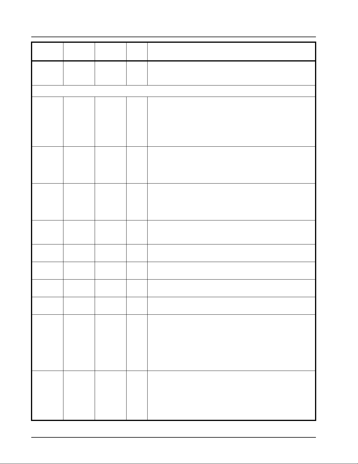
MODEM OR SERIAL I/O INTERFACE
TXA 13 7 O
RXA 11 5 I
RTSA# 36 33 O
T
YPE DESCRIPTION
UART channel B Receiver Ready (active low). This output provides the
RX FIFO/RHR status for receive channel B. See Table 2. If this output
is not used, leave it unconnected.
UART channel A Transmit Data or infrared encoder data. Standard
transmit and receive interface is enabled when MCR[6] = 0. In this
mode, the TX signal will be HIGH during reset or idle (no data). Infrared
IrDA transmit and receive interface is enabled when MCR[6] = 1. In the
Infrared mode, the inactive state (no data) for the Infrared encoder/
decoder interface isLOW. If this output is not used, leave it uncon
nected.
UART channel A Receive Data or infrared receive data. Normal receive
data input must idle HIGH. The infrared receiver pulses typically idles
LOW but can be inverted by software control prior going in to the
decoder, see MCR[6] and FCTR[2]. If this pin is not used, tie it to VCC
or pull it high via a 100k ohm resistor.
UART channel A Request-to-Send (active low) or general purpose output. This output must be asserted prior to using auto RTS flow control,
see EFR[6], MCR[1], FCTR[1:0], EMSR[5:4] and IER[6]. For auto
RS485 half-duplex direction control, see FCTR[3]. If this output is not
used, leave it unconnected.
-
CTSA# 40 38 I
DTRA# 37 34 O
DSRA# 41 39 I
CDA# 42 40 I
RIA# 43 41 I
OP2A# 35 32 O
TXB 14 8 O
UART channel A Clear-to-Send (active low) or general purpose input.
It can be used for auto CTS flow control, see EFR[7], and IER[7]. This
input should be connected to VCC when not used.
UART channel A Data-Terminal-Ready (active low) or general purpose
output. If this output is not used, leave it unconnected.
UART channel A Data-Set-Ready (active low) or general purpose input.
This input should be connected to VCC when not used.
UART channel A Carrier-Detect (active low) or general purpose input.
This input should be connected to VCC when not used.
UART channel A Ring-Indicator (active low) or general purpose input.
This input should be connected to VCC when not used.
Output Port 2 Channel A - The output state is defined by the user and
through the software setting of MCR[3]. INTA is set to the active mode
and OP2A# output is LOW when MCR[3] is set to a logic 1. INTA is set
to the three state mode and OP2A# is HIGH when MCR[3] is set to a
logic 0. See MCR[3]. This output can only be used as a general pur
pose output when interrupts are not used, otherwise it will disturb the
INTA output functionality. If this output is not used, leave it uncon
-
nected.
UART channel B Transmit Data or infrared encoder data. Standard
transmit and receive interface is enabled when MCR[6] = 0. In this
mode, the TX signal will be HIGH during reset or idle (no data). Infrared
IrDA transmit and receive interface is enabled when MCR[6] = 1. In the
Infrared mode, the inactive state (no data) for the Infrared encoder/
decoder interface is LOW. If this output is not used, leave it uncon
-
nected.
4
Page 5
xr XR16C2850
REV. 2.1.3 2.97V TO 5.5V DUAL UART WITH 128-BYTE FIFOS
NAME
RXB 10 4 I
RTSB# 27 22 O
CTSB# 28 23 I
DTRB# 38 35 O
DSRB# 25 20 I
CDB# 21 16 I
RIB# 26 21 I
44-PLCC
IN #
P
48-TQFP
PIN #
T
YPE DESCRIPTION
UART channel B Receive Data or infrared receive data. Normal receive
data input must idle HIGH. The infrared receiver pulses typically idles
LOW but can be inverted by software control prior going in to the
decoder, see MCR[6] and FCTR[2]. If this pin is not used, tie it to VCC
or pull it high via a 100k ohm resistor.
UART channel B Request-to-Send (active low) or general purpose output. This port must be asserted prior to using auto RTS flow control,
see EFR[6], MCR[1], FCTR[1:0], EMSR[5:4] and IER[6]. For auto
RS485 half-duplex direction control, see FCTR[3] and EMSR[3]. If this
output is not used, leave it unconnected.
UART channel B Clear-to-Send (active low) or general purpose input.
It can be used for auto CTS flow control, see EFR[7], and IER[7]. This
input should be connected to VCC when not used.
UART channel B Data-Terminal-Ready (active low) or general purpose
output. If this output is not used, leave it unconnected.
UART channel B Data-Set-Ready (active low) or general purpose input.
This input should be connected to VCC when not used. This input has
no effect on the UART.
UART channel B Carrier-Detect (active low) or general purpose input.
This input should be connected to VCC when not used. This input has
no effect on the UART.
UART channel B Ring-Indicator (active low) or general purpose input.
This input should be connected to VCC when not used. This input has
no effect on the UART.
OP2B# 15 9 O
ANCILLARY SIGNALS
XTAL1 18 13 I Crystal or external clock input.
XTAL2 19 14 O Crystal or buffered clock output.
HDCNTL# - 37 I RS-485 half duplex directional control for channel A and B (active low).
Output Port 2 Channel B - The output state is defined by the user and
through the software setting of MCR[3]. INTB is set to the active mode
and OP2B# output is LOW when MCR[3] is set to a logic 1. INTB is set
to the three state mode and OP2B# is HIGH when MCR[3] is set to a
logic 0. See MCR[3]. This output can only be used as a general pur
pose output when interrupts are not used, otherwise it will disturb the
INTB output functionality. If this output is not used, leave it uncon
nected.
Connect to VCC for normal RTS# function and connect to GND for RS485 half duplex direction control. RTS# pin goes LOW for transmit and
HIGH for receive during RS-485 mode. This pin is wire “OR-ed” with
FCTR[3]. If this pin is connected to VCC, the function of the RTS# pin
can be controlled via FCTR[3]. If this pin is connected to GND, the
RTS# pin will always be the RS-485 half duplex direction control and
can not be controlled via FCTR[3]. See FCTR[3].
-
-
5
Page 6
XR16C2850 xr
2.97V TO 5.5V DUAL UART WITH 128-BYTE FIFOS REV. 2.1.3
NAME
44-PLCC
IN #
P
48-TQFP
PIN #
T
YPE DESCRIPTION
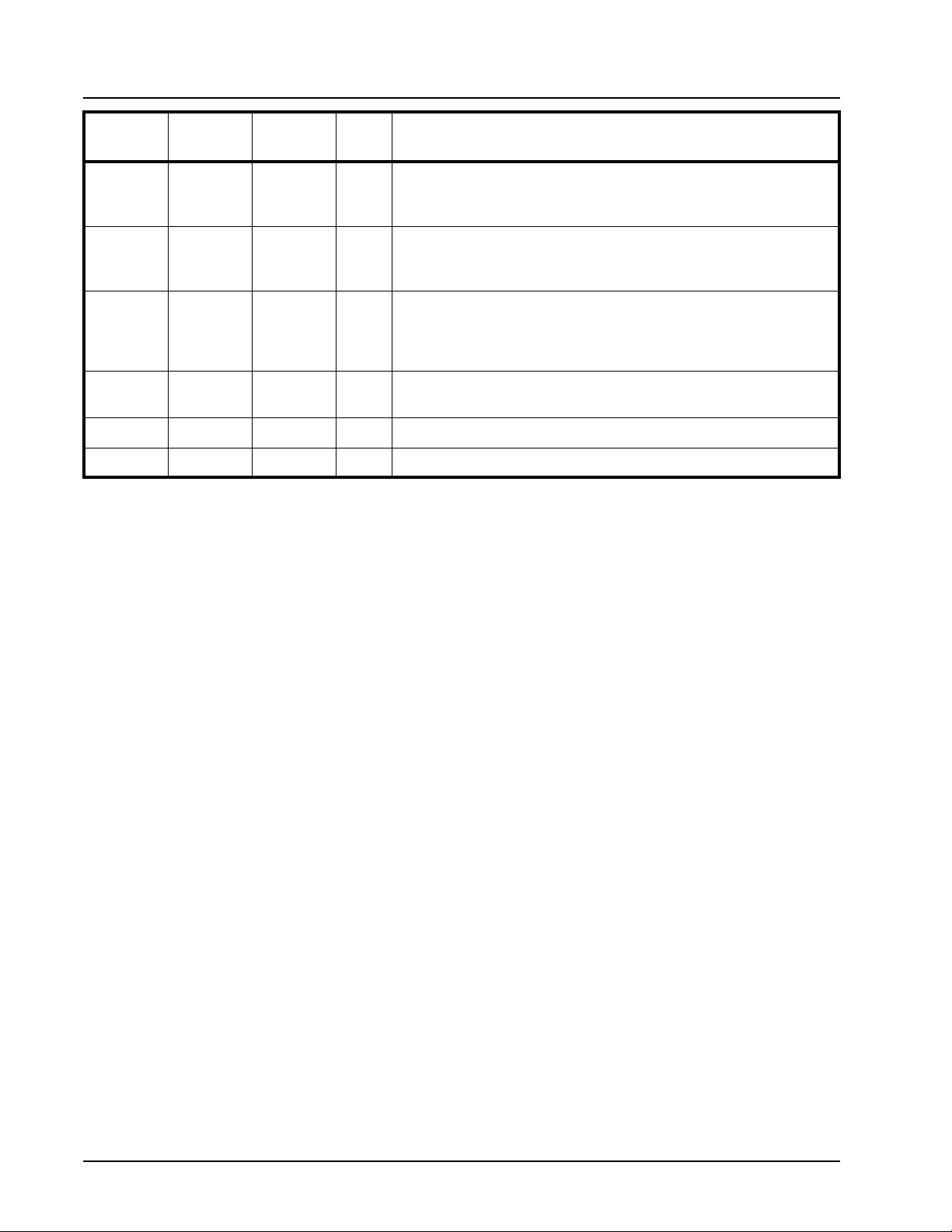
CLKSEL - 25 I Clock Pre-scaler select. Connect to VCC for divide by 1 and GND for
divide by 4. MCR[7] can override the state of this pin following reset or
initialization. See Figure 6 and MCR[7].
CLK8/16 - 24 I Transmit/Receive data sampling rate. Connect to VCC for normal 16X
sampling clock (standard baud rates) or GND for 8X sampling clock to
double the standard baud rates.
RESET 39 36 I Reset (active high) - A longer than 40 ns HIGH pulse on this pin will
reset the internal registers and all outputs. The UART transmitter output
will be held at logic 1, the receiver input will be ignored and outputs are
reset during reset period (see
Table 16).
VCC 44 42 Pwr 2.97V to 5.5V power supply. All inputs are 5V tolerant for devices with
top mark date code of "F2 YYWW" and newer.
GND 22 17 Pwr Power supply common, ground.
N.C. none 12 No Connection.
Pin type: I=Input, O=Output, I/O= Input/output, OD=Output Open Drain.
6
Page 7

xr XR16C2850
REV. 2.1.3 2.97V TO 5.5V DUAL UART WITH 128-BYTE FIFOS
1.0 PRODUCT DESCRIPTION
The XR16C2850 (2850) integrates the functions of 2 enhanced 16C550 Universal Asynchrounous Receiver
and Transmitter (UART). Each UART is independently controlled having its own set of device configuration
registers. The configuration registers set is 16550 UART compatible for control, status and data transfer.
Additionally, each UART channel has 128-bytes of transmit and receive FIFOs, automatic RTS/CTS hardware
flow control with hysteresis control, automatic Xon/Xoff and special character software flow control,
programmable transmit and receive FIFO trigger levels, FIFO level counters, infrared encoder and decoder
(IrDA ver 1.0), programmable baud rate generator with a prescaler of divide by 1 or 4, and data rate up to 6.25
Mbps with 8X sampling clock rate (available only in the 48-pin TQFP package) or 3.125Mbps in the 16X rate.
The XR16C2850 is a 5V and 3.3V device. The 2850 is fabricated with an advanced CMOS process.
Enhanced Features
The 2850 DUART provides a solution that supports 128 bytes of transmit and receive FIFO memory, instead of
64 bytes provided in the XR16L2750 and 16 bytes in the ST16C2550, or one byte in the ST16C2450. The
2850 is designed to work with high performance data communication systems, that require fast data
processing time. Increased performance is realized in the 2850 by the larger transmit and receive FIFOs, FIFO
trigger level control, FIFO level counters and automatic flow control mechanism. This allows the external
processor to handle more networking tasks within a given time. For example, the ST16C2550 with a 16 byte
FIFO, unloads 16 bytes of receive data in 1.53 ms (This example uses a character length of 11 bits, including
start/stop bits at 115.2Kbps). This means the external CPU will have to service the receive FIFO at 1.53 ms
intervals. However with the 128 byte FIFO in the 2850, the data buffer will not require unloading/loading for
12.2 ms. This increases the service interval giving the external CPU additional time for other applications and
reducing the overall UART interrupt servicing time. In addition, the programmable FIFO level trigger interrupt
and automatic hardware/software flow control is uniquely provided for maximum data throughput performance
especially when operating in a multi-channel system. The combination of the above greatly reduces the CPU’s
bandwidth requirement, increases performance, and reduces power consumption.
The 2850 supports a half-duplex output direction control signaling pin, RTS# A/B, to enable and disable the
external RS-485 transceiver operation. It automatically switches the logic state of the output pin to the receive
state after the last stop-bit of the last character has been shifted out of the transmitter. After receiving, the logic
state of the output pin switches back to the transmit state when a data byte is loaded in the transmitter. The
auto RS-485 direction control pin is not activated after reset. To activate the direction control function, user has
to set FCTR Bit-3 to “1”. This pin is normally high for receive state, low for transmit state.
Data Rate
The 2850 is capable of operation up to 3.125 Mbps at 5V with 16X internal sampling clock rate, and 6.25 Mbps
at 5V with 8X sampling clock rate (available only on the 48-pin package). The device can operate with an
external 24 MHz crystal on pins XTAL1 and XTAL2, or external clock source of up to 50 MHz on XTAL1 pin.
With a typical crystal of 14.7456 MHz and through a software option, the user can set the prescaler bit for data
rates of up to 1.84 Mbps.
The rich feature set of the 2850 is available through the internal registers. Automatic hardware/software flow
control, selectable transmit and receive FIFO trigger levels, selectable TX and RX baud rates, infrared
encoder/decoder interface, modem interface controls, and a sleep mode are all standard features.
Following a power on reset or an external reset, the 2850 is software compatible with previous generation of
UARTs, 16C2450, 16C2550 and 16L2750.
7
Page 8
XR16C2850 xr
2.97V TO 5.5V DUAL UART WITH 128-BYTE FIFOS REV. 2.1.3
2.0 FUNCTIONAL DESCRIPTIONS
2.1 CPU Interface
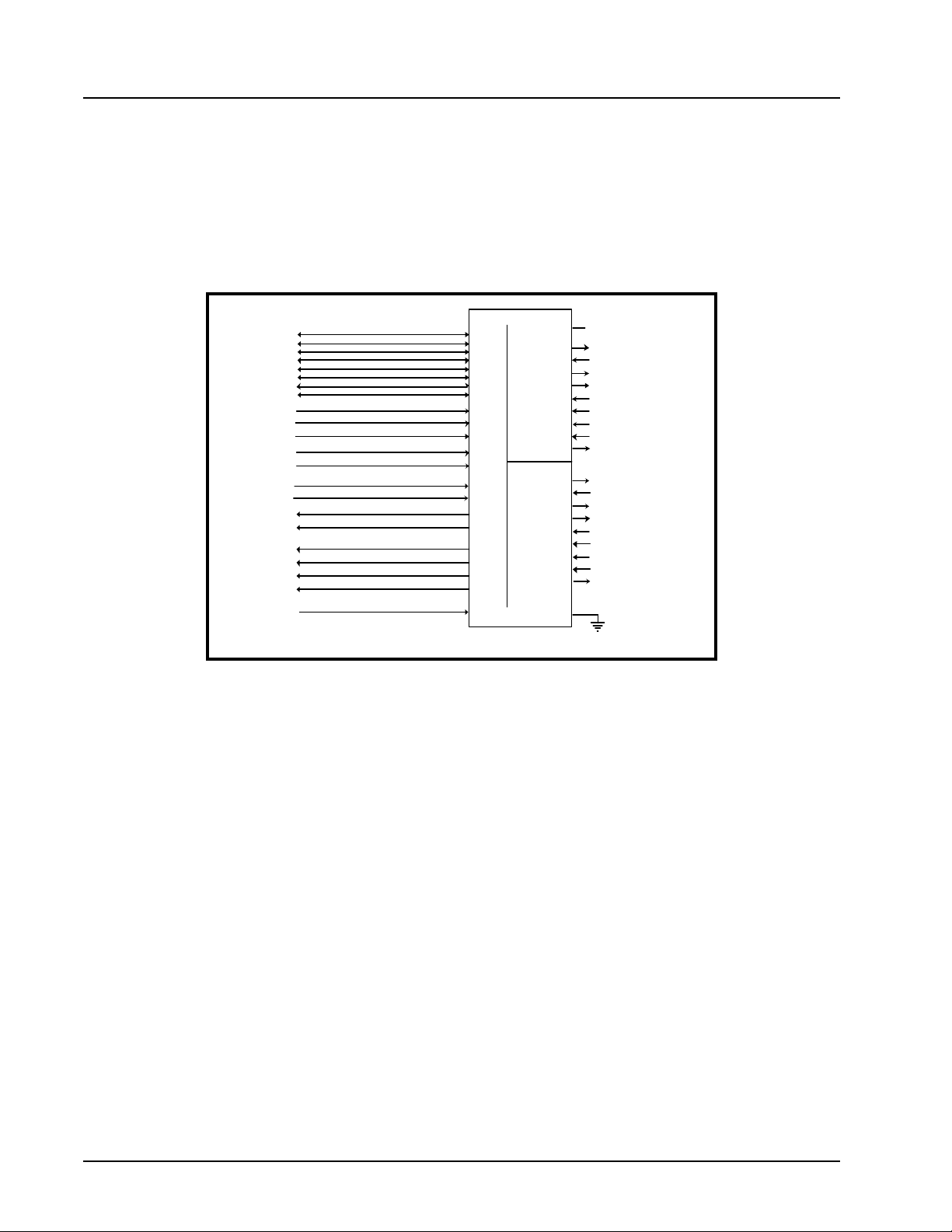
The CPU interface is 8 data bits wide with 3 address lines and control signals to execute data bus read and
write transactions. The 2850 data interface supports the Intel compatible types of CPUs and it is compatible to
the industry standard 16C550 UART. No clock (oscillator nor external clock) is required to operate a data bus
transaction. Each bus cycle is asynchronous using CS#, IOR# and IOW# signals. Both UART channels share
the same data bus for host operations. The data bus interconnections are shown in
Figure 3.
FIGURE 3. XR16C2850 DATA BUS INTERCONNECTIONS
VCC
UART
Channel A
UART
Channel B
DTRA #
RTS A #
CTS A #
DSRA#
CDA#
OP2A#
DTRB #
RTS B #
CTS B #
DSRB#
CDB#
OP2B#
GND
VCC
TXA
RXA
RI A #
TXB
RXB
RI B #
Seri al I nter face of
RS- 232 , RS- 4 85
Serial Interface of RS-
232, RS-485
2750int
D0
D1
D2
D3
D4
D5
D6
D7
A0
A1
A2
IOR#
IOW#
UART _CS A #
UART _CS B #
UART _I NT A
UART _I NT B
TXRDYA#
RXRDYA #
TXRDYB#
RXRDYB #
UART_RESET RESE T
D0
D1
D2
D3
D4
D5
D6
D7
A0
A1
A2
IOR#
IOW#
CSA#
CSB#
INTA
INTB
TX RDY A#
RXRDYA #
TX RDY B#
RXRDYB #
.
2.2 Device Reset
The RESET input resets the internal registers and the serial interface outputs in both channels to their default
state (see
Ta bl e 16). An active high pulse of longer than 40 ns duration will be required to activate the reset
function in the device.
2.3 Device Identification and Revision
The XR16C2850 provides a Device Identification code and a Device Revision code to distinguish the part from
other devices and revisions. To read the identification code from the part, it is required to set the baud rate
generator registers DLL and DLM both to 0x00. Now reading the content of the DLM will provide 0x12 for the
XR16C2850 and reading the content of DLL will provide the revision of the part; for example, a reading of 0x01
means revision A.
2.4 Channel A and B Selection
The UART provides the user with the capability to bi-directionally transfer information between an external
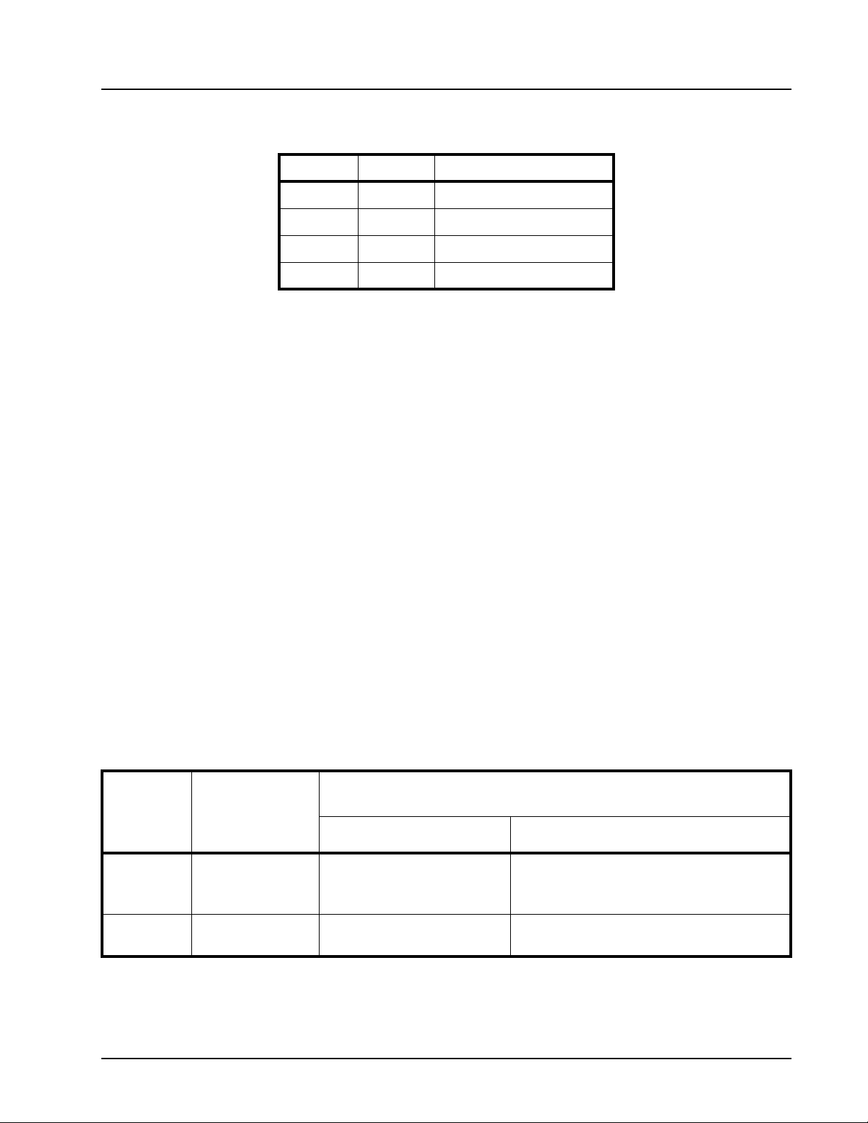
CPU and an external serial communication device. A logic 0 on chip select pins, CSA# or CSB#, allows the
user to select UART channel A or B to configure, send transmit data and/or unload receive data to/from the
UART. Selecting both UARTs can be useful during power up initialization to write to the same internal registers,
but do not attempt to read from both uarts simultaneously. Individual channel select functions are shown in
Table 1.
8
Page 9
xr XR16C2850
REV. 2.1.3 2.97V TO 5.5V DUAL UART WITH 128-BYTE FIFOS
TABLE 1: CHANNEL A AND B SELECT
CSA# CSB# FUNCTION
1 1 UART de-selected
0 1 Channel A selected
1 0 Channel B selected
0 0 Channel A and B selected
2.5 Channel A and B Internal Registers
Each UART channel in the 2850 has a set of enhanced registers for control, monitoring and data loading and
unloading. The configuration register set is compatible to those already available in the standard single
16C550 and dual ST16C2550. These registers function as data holding registers (THR/RHR), interrupt status
and control registers (ISR/IER), a FIFO control register (FCR), receive line status and control registers (LSR/
LCR), modem status and control registers (MSR/MCR), programmable data rate (clock) divisor registers (DLL/
DLM), and a user accessible scratchpad register (SPR).
Beyond the general 16C2550 features and capabilities, the 2850 offers enhanced feature registers (EMSR,
FLVL, EFR, Xon/Xoff 1, Xon/Xoff 2, FCTR, TRG, FC) that provide automatic RTS and CTS hardware flow
control, Xon/Xoff software flow control, automatic RS-485 half-duplex direction output enable/disable, FIFO
trigger level control, and FIFO level counters. All the register functions are discussed in full detail later in
“Section 3.0, UART INTERNAL REGISTERS” on page 21.
2.6 DMA Mode
The device does not support direct memory access. The DMA Mode (a legacy term) in this document doesn’t
mean “direct memory access” but refers to data block transfer operation. The DMA mode affects the state of
the RXRDY# A/B and TXRDY# A/B output pins. The transmit and receive FIFO trigger levels provide additional
flexibility to the user for block mode operation. The LSR bits 5-6 provide an indication when the transmitter is
empty or has an empty location(s) for more data. The user can optionally operate the transmit and receive
FIFO in the DMA mode (FCR bit-3=1). When the transmit and receive FIFO are enabled and the DMA mode is
disabled (FCR bit-3 = 0), the 2850 is placed in single-character mode for data transmit or receive operation.
When DMA mode is enabled (FCR bit-3 = 1), the user takes advantage of block mode operation by loading or
unloading the FIFO in a block sequence determined by the programmed trigger level. In this mode, the 2850
sets the TXRDY# pin when the transmit FIFO becomes full, and sets the RXRDY# pin when the receive FIFO
becomes empty. The following table shows their behavior. Also see Figures
20 through 25.
PINS
RXRDY# A/B
TXRDY# A/B
TABLE 2: TABLE 2TXRDY# AND RXRDY# OUTPUTS IN FIFO AND DMA MODE
FCR BIT-0=0
(FIFO DISABLED)
LOW = 1 byte
HIGH = no data
LOW = THR empty
HIGH = byte in THR
FCR Bit-3 = 0
(DMA Mode Disabled)
LOW = at least 1 byte in FIFO
HIGH = FIFO empty
LOW = FIFO empty
HIGH = at least 1 byte in FIFO
FCR BIT-0=1 (FIFO ENABLED)
FCR Bit-3 = 1
(DMA Mode Enabled)
HIGH to LOW transition when FIFO reaches
the trigger level, or timeout occurs.
LOW to HIGH transition when FIFO empties.
LOW = FIFO has at least 1 empty location
HIGH = FIFO is full
9
Page 10
XR16C2850 xr
2.97V TO 5.5V DUAL UART WITH 128-BYTE FIFOS REV. 2.1.3
2.7 INTA and INTB Ouputs
The INTA and INTB interrupt output output changes according to the operating mode and enahnced features
setup.
Table 3 and 4 summarize the operating behavior for the transmitter and receiver. Also see Figures 20
through 25.
TABLE 3: INTA AND INTB PINS OPERATION FOR TRANSMITTER
Auto RS485
Mode
INTA/B Pin NO LOW = a byte in THR
INTA/B Pin YES LOW = a byte in THR
FCR BIT-0 = 0
(FIFO DISABLED)
HIGH = THR empty
HIGH = transmitter empty
FCR BIT-0 = 1
(FIFO ENABLED)
LOW = FIFO above trigger level
HIGH = FIFO below trigger level or FIFO empty
LOW = FIFO above trigger level
HIGH = FIFO below trigger level or transmitter empty
TABLE 4: INTA AND INTB PIN OPERATION FOR RECEIVER
FCR BIT-0 = 0
(FIFO DISABLED)
INTA/B Pin LOW = no data
HIGH = 1 byte
LOW = FIFO below trigger level
HIGH = FIFO above trigger level
FCR BIT-0 = 1
(FIFO ENABLED)
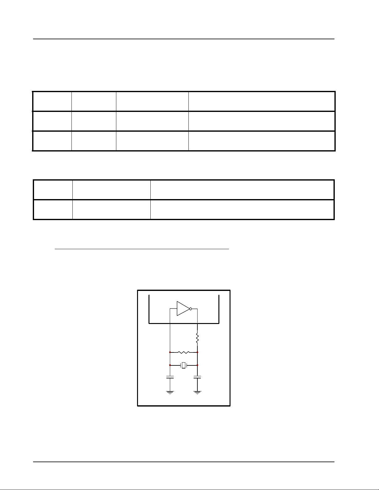
2.8 Crystal Oscillator or External Clock Input
The 2850 includes an on-chip oscillator (XTAL1 and XTAL2) to produce a clock for both UART sections in the
device.
The CPU data bus does not require this clock for bus operation. The crystal oscillator provides a
system clock to the Baud Rate Generators (BRG) section found in each of the UART. XTAL1 is the input to the
oscillator or external clock buffer input with XTAL2 pin being the output.
SEE”PROGRAMMABLE BAUD
RATE GENERATOR” ON PAGE 11.
FIGURE 4. TYPICAL OSCILLATOR CONNECTIONS
XTAL 1 XTAL 2
R2
500 ΚΩ − 1 ΜΩ
C1
22-47 pF
22-47 pF
C2
Y1
R1
0-120 Ω
(Optional)
1.8432 MHz
to
24 MHz
The on-chip oscillator is designed to use an industry standard microprocessor crystal (parallel resonant,
fundamental frequency with 10-22 pF capacitance load, ESR of 20-120 ohms and 100 ppm frequency
tolerance) connected externally between the XTAL1 and XTAL2 pins (see
Figure 4). Alternatively, an external
clock can be connected to the XTAL1 pin to clock the internal baud rate generator for standard or custom rates.
10
Page 11
xr XR16C2850
REV. 2.1.3 2.97V TO 5.5V DUAL UART WITH 128-BYTE FIFOS
Typical oscillator connections are shown in Figure 4. For further reading on oscillator circuit please see
application note DAN108 on EXAR’s web site.
2.9 Programmable Baud Rate Generator
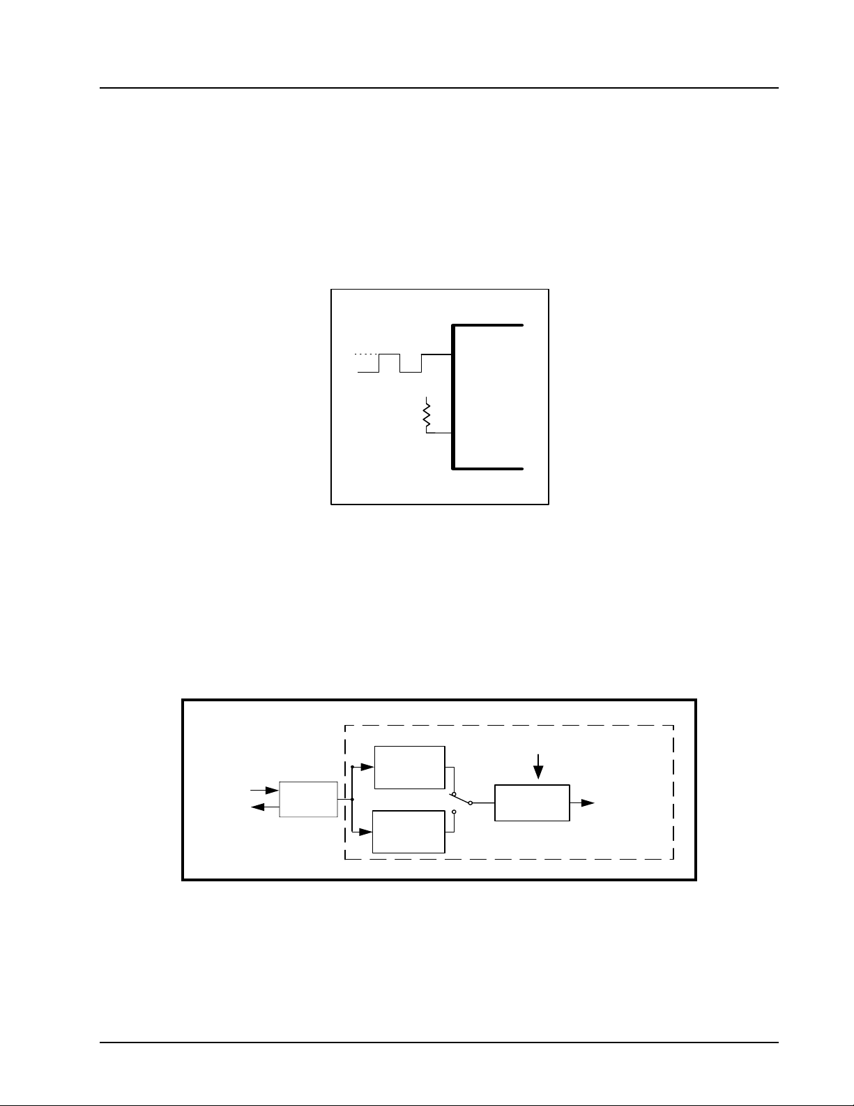
A single Baud Rate Generator (BRG) is provided for the transmitter and receiver, allowing independent TX/RX
channel control. The programmable Baud Rate Generator is capable of operating with a crystal frequency of
up to 24 MHz. However, with an external clock input on XTAL1 pin and a 2K ohms pull-up resistor on XTAL2
pin (as shown in
sampling) at room temperature and 5.0V.
FIGURE 5. EXTERNAL CLOCK CONNECTION FOR EXTENDED DATA RATE
Figure 5) it can extend its operation up to 50 MHz (3.125 Mbps serial data rate and 16X
External Clock
vcc
gnd
VCC
R1
2K
XTAL1
XTAL2
Each UART also has their own prescaler along with the BRG. The prescaler is controlled by CLKSEL hardware
pin or a software bit in the MCR register. The MCR register bit-7 sets the prescaler to divide the input crystal or
external clock by 1 or 4 and can override the CLKSEL pin following reset. The clock output of the prescaler
goes to the BRG. The BRG further divides this clock by a programmable divisor between 1 and (2
16
-1) to
obtain a 16X sampling rate clock of the serial data rate. The sampling rate clock is used by the transmitter for
data bit shifting and
receiver for data sampling.
FIGURE 6. BAUD RATE GENERATOR AND PRESCALER
DLL and DLM
Registers
MCR Bit-7=0
(default)
Baud Rate
Generator
MCR Bit-7=1
Logic
16X
Sampling
Rate Clock to
Transmitter
XTAL1
XTAL2
Prescaler
Divide by 1
Crystal
Osc/
Buffer
Prescaler
Divide by 4
Programming the Baud Rate Generator Registers DLM and DLL provides the capability of selecting the
operating data rate.
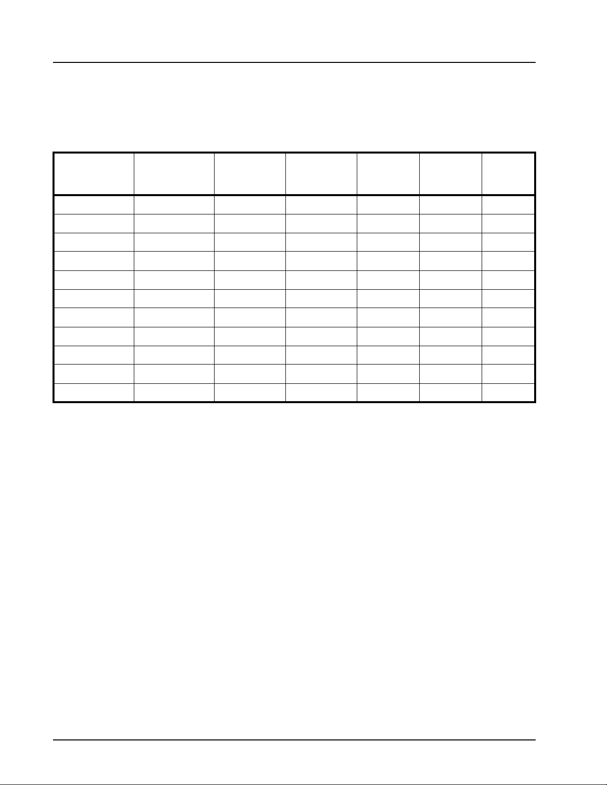
Tab le 5 shows the standard data rates available with a 14.7456 MHz crystal or external
clock at 16X sampling rate clock rate. A 16X sampling clock is typically used. However, user can select the 8X
sampling clock rate mode to double the operating data rate. When using a non-standard data rate crystal or
external clock, the divisor value can be calculated for DLL/DLM with the following equation.
11
Page 12
XR16C2850 xr
2.97V TO 5.5V DUAL UART WITH 128-BYTE FIFOS REV. 2.1.3
divisor (decimal) = (XTAL1 clock frequency / prescaler) / (serial data rate x 16), with CLK8/16 pin = 1
divisor (decimal) = (XTAL1 clock frequency / prescaler) / (serial data rate x 8), with CLK8/16 pin = 0
TABLE 5: TYPICAL DATA RATES WITH A 14.7456 MHZ CRYSTAL OR EXTERNAL CLOCK
OUTPUT Data Rate
MCR Bit-7=1
100 400 2304 900 09 00 0
600 2400 384 180 01 80 0
1200 4800 192 C0 00 C0 0
2400 9600 96 60 00 60 0
4800 19.2k 48 30 00 30 0
9600 38.4k 24 18 00 18 0
19.2k 76.8k 12 0C 00 0C 0
38.4k 153.6k 6 06 00 06 0
57.6k 230.4k 4 04 00 04 0
115.2k 460.8k 2 02 00 02 0
230.4k 921.6k 1 01 00 01 0
OUTPUT Data Rate
MCR Bit-7=0
(DEFAULT)
DIVISOR FOR 16x
Clock (Decimal)
DIVISOR FOR 16x
Clock (HEX)
DLM
PROGRAM
VALUE (HEX)
DLL
PROGRAM
VALUE (HEX)
DATA RATE
ERROR (%)
2.10 Transmitter
The transmitter section comprises of an 8-bit Transmit Shift Register (TSR) and 128 bytes of FIFO which
includes a byte-wide Transmit Holding Register (THR). TSR shifts out every data bit with the 16X/8X internal
clock. A bit time is 16 (8) clock periods (see CLK8/16 pin description). The transmitter sends the start-bit
followed by the number of data bits, inserts the proper parity-bit if enabled, and adds the stop-bit(s). The status
of the FIFO and TSR are reported in the Line Status Register (LSR bit-5 and bit-6).
2.10.1 Transmit Holding Register (THR) - Write Only
The transmit holding register is an 8-bit register providing a data interface to the host processor. The host
writes transmit data byte to the THR to be converted into a serial data stream including start-bit, data bits,
parity-bit and stop-bit(s). The least-significant-bit (Bit-0) becomes first data bit to go out. The THR is the input
register to the transmit FIFO of 128 bytes when FIFO operation is enabled by FCR bit-0. Every time a write
operation is made to the THR, the FIFO data pointer is automatically bumped to the next sequential data
location.
2.10.2 Transmitter Operation in non-FIFO Mode
The host loads transmit data to THR one character at a time. The THR empty flag (LSR bit-5) is set when the
data byte is transferred to TSR. THR flag can generate a transmit empty interrupt (ISR bit-1) when it is enabled
by IER bit-1. The TSR flag (LSR bit-6) is set when TSR becomes completely empty.
12
Page 13
xr XR16C2850
REV. 2.1.3 2.97V TO 5.5V DUAL UART WITH 128-BYTE FIFOS
FIGURE 7. TRANSMITTER OPERATION IN NON-FIFO MODE
Data
Byte
Transmit
Holding
Register
(THR)
THR Interrupt (ISR bit-1)
Enabled by IER bit-1
16X or 8X
Clock
Transmit Shift Register (TSR)
M
S
B
L
S
B
TXNOFIFO1
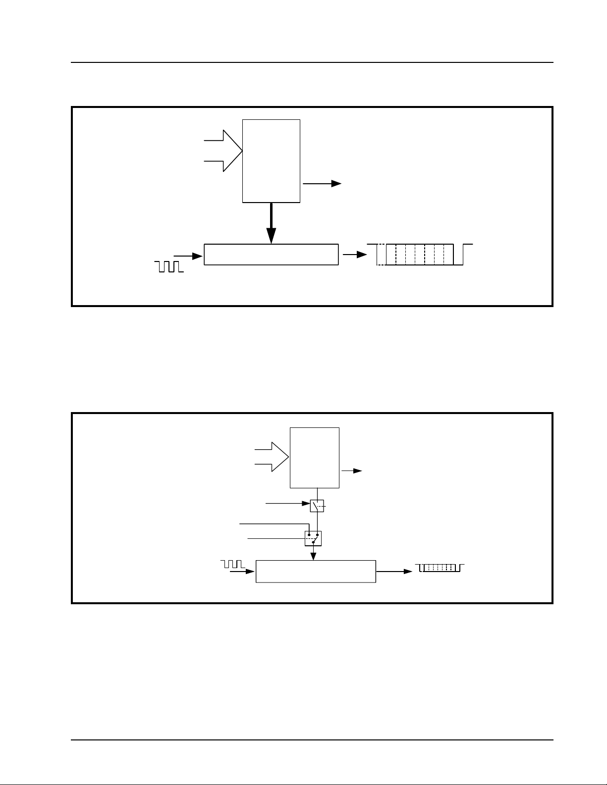
2.10.3 Transmitter Operation in FIFO Mode
The host may fill the transmit FIFO with up to 128 bytes of transmit data. The THR empty flag (LSR bit-5) is set
whenever the FIFO is empty. The THR empty flag can generate a transmit empty interrupt (ISR bit-1) when the
amount of data in the FIFO falls below its programmed trigger level. The transmit empty interrupt is enabled by
IER bit-1. The TSR flag (LSR bit-6) is set when TSR/FIFO becomes empty.
FIGURE 8. TRANSMITTER OPERATION IN FIFO AND FLOW CONTROL MODE
Transmit
Data Byte
Auto CTS Flow Control (CTS# pin)
Flow Control Characters
(Xoff1/2 and Xon1/2 Reg.
Auto Software Flow Control
16X or 8X
Clock
Transmit
FIFO
Transm it Data Shift Register
(TSR)
THR Interrupt (ISR bit-1) falls
below the programmed Trigger
Level and then when becomes
empty. FIFO is Enabled by FCR
bit-0=1
TXFIFO1
13
Page 14
XR16C2850 xr
2.97V TO 5.5V DUAL UART WITH 128-BYTE FIFOS REV. 2.1.3
2.11 Receiver
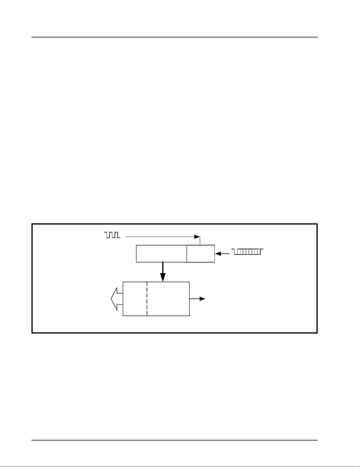
The receiver section contains an 8-bit Receive Shift Register (RSR) and 128 bytes of FIFO which includes a
byte-wide Receive Holding Register (RHR). The RSR uses the 16X/8X clock (CLK8/16 pin) for timing. It
verifies and validates every bit on the incoming character in the middle of each data bit. On the falling edge of
a start or false start bit, an internal receiver counter starts counting at the 16X/8X clock rate. After 8 clocks (or
4 if 8X) the start bit period should be at the center of the start bit. At this time the start bit is sampled and if it is
still a logic 0 it is validated. Evaluating the start bit in this manner prevents the receiver from assembling a false
character. The rest of the data bits and stop bits are sampled and validated in this same manner to prevent
false framing. If there were any error(s), they are reported in the LSR register bits 2-4. Upon unloading the
receive data byte from RHR, the receive FIFO pointer is bumped and the error tags are immediately updated to
reflect the status of the data byte in RHR register. RHR can generate a receive data ready interrupt upon
receiving a character or delay until it reaches the FIFO trigger level. Furthermore, data delivery to the host is
guaranteed by a receive data ready time-out interrupt when data is not received for 4 word lengths as defined
by LCR[1:0] plus 12 bits time. This is equivalent to 3.7-4.6 character times. The RHR interrupt is enabled by
IER bit-0.
2.11.1 Receive Holding Register (RHR) - Read-Only
The Receive Holding Register is an 8-bit register that holds a receive data byte from the Receive Shift
Register. It provides the receive data interface to the host processor. The RHR register is part of the receive
FIFO of 128 bytes by 11-bits wide, the 3 extra bits are for the 3 error tags to be reported in LSR register. When
the FIFO is enabled by FCR bit-0, the RHR contains the first data character received by the FIFO. After the
RHR is read, the next character byte is loaded into the RHR and the errors associated with the current data
byte are immediately updated in the LSR bits 2-4.
FIGURE 9. RECEIVER OPERATION IN NON-FIFO MODE
16X or 8X
Clock
Receive Data Shift
Register (RSR)
Receive
Data Byte
and Errors
Error
Tags in
LSR bits
4:2
Receive Data
Holding Register
(RHR)
Data Bit
Validation
Receive Data Characters
RHR Interrupt (ISR bit-2)
RXFIFO1
14
Page 15
xr XR16C2850
REV. 2.1.3 2.97V TO 5.5V DUAL UART WITH 128-BYTE FIFOS
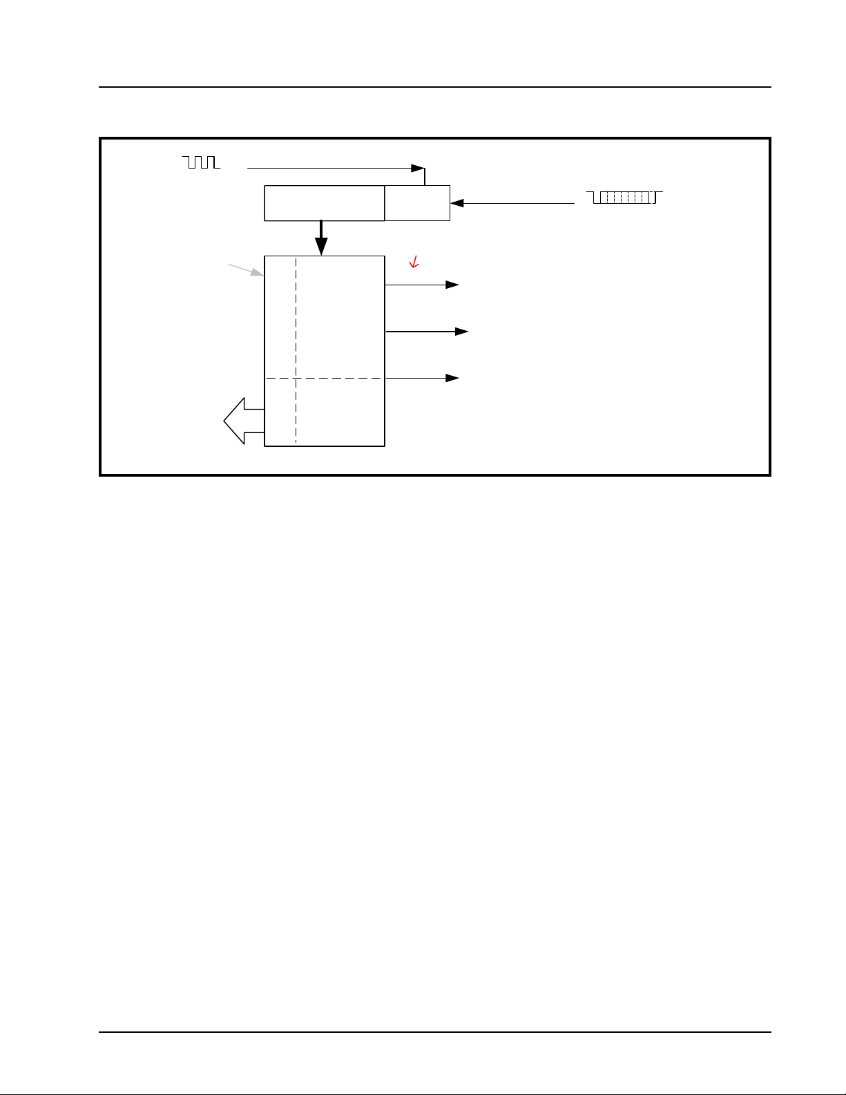
FIGURE 10. RECEIVER OPERATION IN FIFO AND AUTO RTS FLOW CONTROL MODE
16X or 8X
Clock
128 bytes by 11-bit
wide FIFO
Receive Data
Byte and Errors
Receive Data Shift
Register (RSR)
Receive
Data FIFO
(128-sets)
Error Tags
Receive
Data
LSR bits 4:2
Error Tags in
Data Bit
Validation
Example:
- RX FIFO trigger level selected at 16 bytes
Data falls to 8
FIFO Trigger=16
Data fills to 24
(See Note Below )
RTS# re-asserts when data falls below the flow
control trigger level to restart remote transmitter.
Enable by EFR bit-6=1, MCR bit-1.
RHR Interrupt (ISR bit-2) programmed for
desired FIFO trigger level.
FIFO is Enabled by FCR bit-0=1
RTS# de-asserts when data fills above the flow
control trigger level to suspend remote transmitter.
Enable by EFR bit-6=1, MCR bit-1.
Receive Data Characters
RXFIFO1
NOTE: Table-B selected as Trigger Table for Figure 10 (Table 10).
2.12 Auto RTS (Hardware) Flow Control
Automatic RTS hardware flow control is used to prevent data overrun to the local receiver FIFO. The RTS#
output is used to request remote unit to suspend/resume data transmission. The auto RTS flow control
features is enabled to fit specific application requirement (see
Figure 11):
• Enable auto RTS flow control using EFR bit-6.
• The auto RTS function must be started by asserting RTS output pin (MCR bit-1 to logic 1 after it is enabled).
With the Auto RTS function enabled, the RTS# output pin will not be de-asserted (HIGH) when the receive
FIFO reaches the programmed trigger level, but will be de-asserted when the FIFO reaches the next trigger
level (
See Table 10). The RTS# output pin will be asserted (LOW) again after the FIFO is unloaded to the next
trigger level below the programmed trigger level. However, even under these conditions, the 2850 will continue
to accept data until the receive FIFO is full if the remote UART transmitter continues to send data.
• Enable RTS interrupt through IER bit-6 (after setting EFR bit-4). The UART issues an interrupt when the
RTS# pin is de-asserted (HIGH) during Auto RTS flow control mode: ISR bit-5 will be set to logic 1.
2.13 Auto RTS Hysteresis
The 2850 has a new feature that provides flow control trigger hysteresis while maintaining compatibility with
the XR16C850, ST16C650A and ST16C550 family of UARTs. With the Auto RTS function enabled, an
interrupt is generated when the receive FIFO reaches the programmed RX trigger level. The RTS# pin will not
be forced HIGH (RTS off) until the receive FIFO reaches the upper limit of the hysteresis level. The RTS# pin
will return LOW after the RX FIFO is unloaded to the lower limit of the hysteresis level. Under the above
described conditions, the 2850 will continue to accept data until the receive FIFO gets full. The Auto RTS
function is initiated when the RTS# output pin is asserted LOW (RTS On).
details for the Auto RTS# Hysteresis levels. Please note that this table is for programmable trigger levels only
(Table D). The hysteresis values for Tables A-C are the next higher and next lower trigger levels in the
corresponding table.
Tab le 13 shows the complete
15
Page 16
XR16C2850 xr
2.97V TO 5.5V DUAL UART WITH 128-BYTE FIFOS REV. 2.1.3
2.14 Auto CTS Flow Control
Automatic CTS flow control is used to prevent data overrun to the remote receiver FIFO. The CTS# input is
monitored to suspend/restart the local transmitter. The auto CTS flow control feature is selected to fit specific
application requirement (see
Figure 11):
• Enable auto CTS flow control using EFR bit-7.
With the Auto CTS function enabled, the UART will suspend transmission as soon as the stop bit of the
character in the Transmit Shift Register has been shifted out. Transmission is resumed after the CTS# input is
re-asserted (LOW), indicating more data may be sent.
• Enable CTS interrupt through IER bit-7 (after setting EFR bit-4). The UART issues an interrupt when the
CTS# pin is de-asserted (HIGH) during Auto CTS flow control mode: ISR bit-5 will be set to 1.
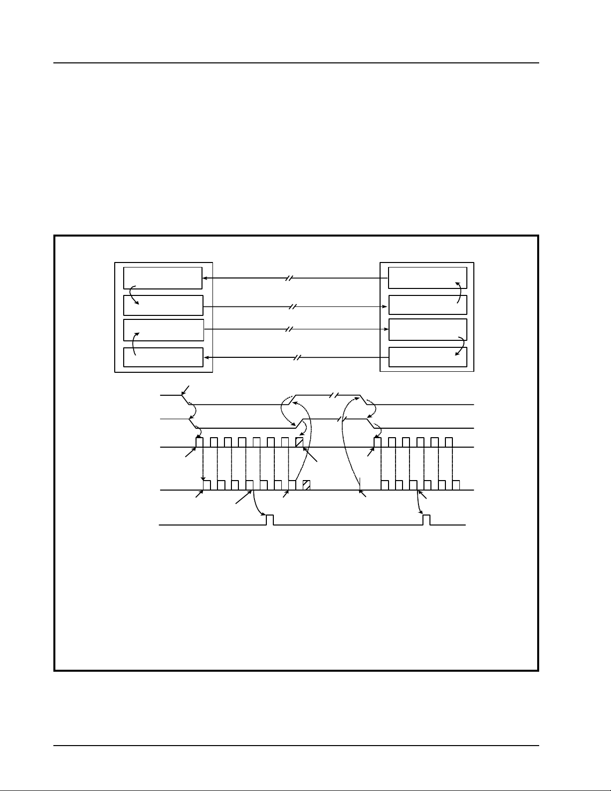
FIGURE 11. AUTO RTS AND CTS FLOW CONTROL OPERATION
Local UART
Receiver FIFO
Trigger Reached
Auto RTS
Trigger Level
Transmitter
Auto CTS
RTSA#
CTSB#
TXB
RXA FIFO
INTA
(RXA FIFO
Interrupt)
UARTA
Monitor
Data Starts
Assert RTS# to Begin
Transmission
1
2
3
4
Receive
Data
RX FIFO
Trigger Level
RXA TXB
RTSA# CTSB#
RXBTXA
RTSB#CTSA#
ON
ON
5
7
RTS High
Threshold
8
6
OFF
OFF
Suspend
Restart
9
RTS Low
Threshold
10
11
Remote UART
UARTB
Transmitter
Auto CTS
Monitor
Receiver FIFO
Trigger Reached
Auto RTS
Trigger Level
ON
ON
RX FIFO
12
Trigger Level
RTSCTS1
The local UART (UARTA) starts data transfer by asserting RTSA# (1). RTSA# is normally connected to CTSB# (2) of
remote UART (UARTB). CTSB# allows its transmitter to send data (3). TXB data arrives and fills UARTA receive FIFO
(4). When RXA data fills up to its receive FIFO trigger level, UARTA activates its RXA data ready interrupt (5) and con
tinues to receive and put data into its FIFO. If interrupt service latency is long and data is not being unloaded, UARTA
monitors its receive data fill level to match the upper threshold of RTS delay and de-assert RTSA# (6). CTSB# follows
(7) and request UARTB transmitter to suspend data transfer. UARTB stops or finishes sending the data bits in its trans
mit shift register (8). When receive FIFO data in UARTA is unloaded to match the lower threshold of RTS delay (9),
UARTA re-asserts RTSA# (10), CTSB# recognizes the change (11) and restarts its transmitter and data flow again until
next receive FIFO trigger (12). This same event applies to the reverse direction when UARTA sends data to UARTB
with RTSB# and CTSA# controlling the data flow.
16
-
-
Page 17
xr XR16C2850
REV. 2.1.3 2.97V TO 5.5V DUAL UART WITH 128-BYTE FIFOS
2.15 Auto Xon/Xoff (Software) Flow Control
When software flow control is enabled (See Table 15), the 2850 compares one or two sequential receive data
characters with the programmed Xon or Xoff-1,2 character value(s). If receive character(s) (RX) match the
programmed values, the 2850 will halt transmission (TX) as soon as the current character has completed
transmission. When a match occurs, the Xoff (if enabled via IER bit-5) flag will be set and the interrupt output
pin will be activated. Following a suspension due to a match of the Xoff character, the 2850 will monitor the
receive data stream for a match to the Xon-1,2 character. If a match is found, the 2850 will resume operation
and clear the flags (ISR bit-4).
Reset initially sets the contents of the Xon/Xoff 8-bit flow control registers to a logic 0. Following reset, any
desired Xon/Xoff value can be used for software flow control. Different conditions can be set to detect Xon/Xoff
characters (
selected, the 2850 compares two consecutive receive characters with two software flow control 8-bit values
(Xon1, Xon2, Xoff1, Xoff2) and controls TX transmissions accordingly. Under the above described flow control
mechanisms, flow control characters are not placed (stacked) in the user accessible RX data buffer or FIFO.
In the event that the receive buffer is overfilling and flow control needs to be executed, the 2850 automatically
sends an Xoff message (when enabled) via the serial TX output to the remote modem. The 2850 sends the
Xoff-1,2 characters two character times (= time taken to send two characters at the programmed baud rate)
after the receive FIFO crosses the programmed trigger level (for all trigger tables A-D). To clear this condition,
the 2850 will transmit the programmed Xon-1,2 characters as soon as receive FIFO is less than one trigger
level below the programmed trigger level (for Trigger Tables A, B, and C) or when receive FIFO is less than the
trigger level minus the hysteresis value (for Trigger Table D). This hysteresis value is the same as the Auto
RTS Hysteresis value in
selected.
See Table 15) and suspend/resume transmissions. When double 8-bit Xon/Xoff characters are
Table 13. Table 6 below explains this when Trigger Table-B (See Tab l e 10) is
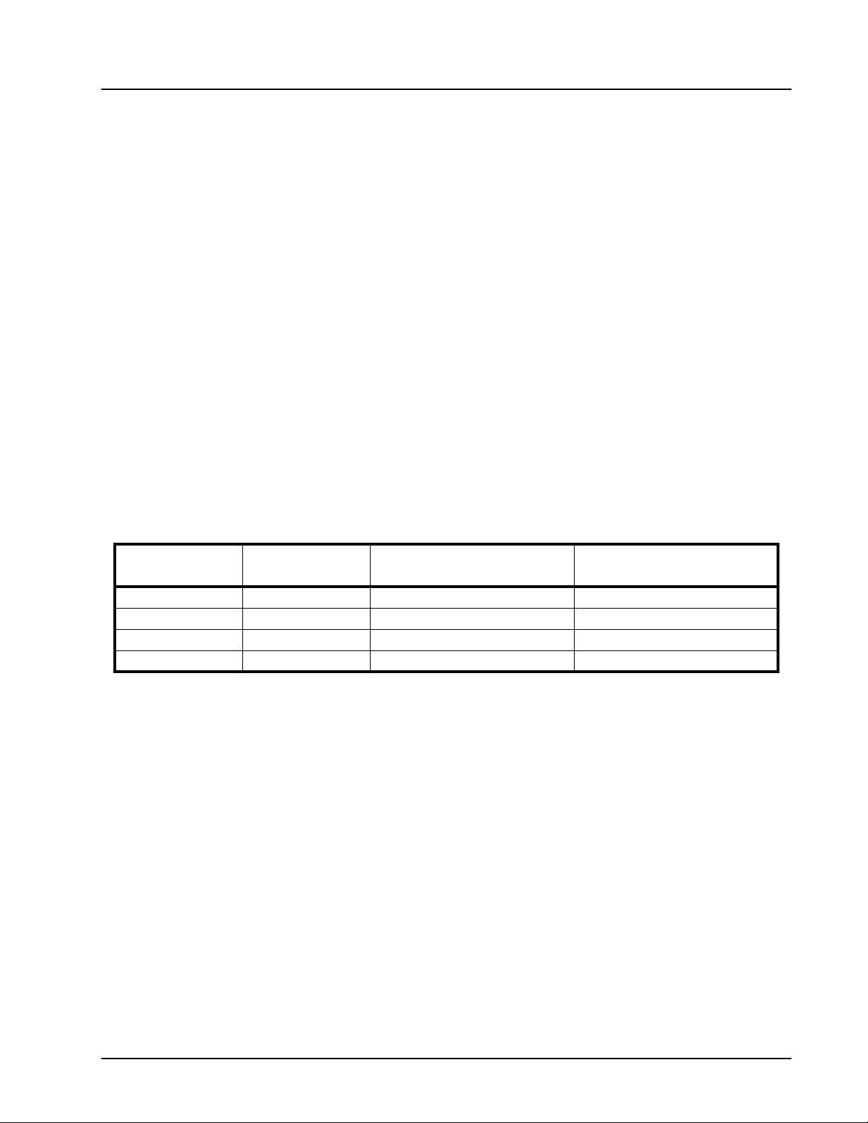
TABLE 6: AUTO XON/XOFF (SOFTWARE) FLOW CONTROL
RX TRIGGER LEVEL INT PIN ACTIVATION
8 8 8* 0
16 16 16* 8
24 24 24* 16
28 28 28* 24
* After the trigger level is reached, an xoff character is sent after a short span of time (= time required to send 2
characters); for example, after 2.083ms has elapsed for 9600 baud and 10-bit word length setting.
XOFF CHARACTER(S) SENT
CHARACTERS IN RX FIFO)
(
XON CHARACTER(S) SENT
CHARACTERS IN RX FIFO)
(
2.16 Special Character Detect
A special character detect feature is provided to detect an 8-bit character when bit-5 is set in the Enhanced
Feature Register (EFR). When this character (Xoff2) is detected, it will be placed in the FIFO along with normal
incoming RX data.
The 2850 compares each incoming receive character with Xoff-2 data. If a match exists, the received data will
be transferred to FIFO and ISR bit-4 will be set to indicate detection of special character. Although the Internal
Register Table shows Xon, Xoff Registers with eight bits of character information, the actual number of bits is
dependent on the programmed word length. Line Control Register (LCR) bits 0-1 defines the number of
character bits, i.e., either 5 bits, 6 bits, 7 bits, or 8 bits. The word length selected by LCR bits 0-1 also
determines the number of bits that will be used for the special character comparison. Bit-0 in the Xon, Xoff
Registers corresponds with the LSB bit for the receive character.
2.17 Auto RS485 Half-duplex Control
The auto RS485 half-duplex direction control changes the behavior of the transmitter when enabled by FCTR
bit-3. It de-asserts RTS# output (HIGH) following
the last stop bit of the last character that has been
transmitted. This helps in turning around the transceiver to receive the remote station’s response. When the
host is ready to transmit next polling data packet again, it only has to load data bytes to the transmit FIFO. The
transmitter automatically re-asserts RTS# output (LOW) prior sending the data.
17
Page 18
XR16C2850 xr
2.97V TO 5.5V DUAL UART WITH 128-BYTE FIFOS REV. 2.1.3
2.18 Infrared Mode
The 2850 UART includes the infrared encoder and decoder compatible to the IrDA (Infrared Data Association)
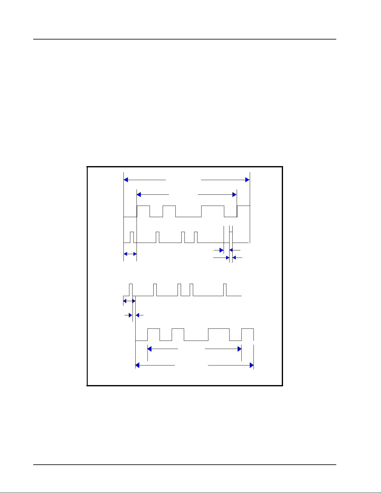
version 1.0. The IrDA 1.0 standard that stipulates the infrared encoder sends out a
3/16 of a bit wide HIGH-
pulse for each “0” bit in the transmit data stream. This signal encoding reduces the on-time of the infrared LED,
hence reduces the power consumption. See
Figure 12 below.
The infrared encoder and decoder are enabled by setting MCR register bit-6 to a ‘1’. When the infrared feature
is enabled, the transmit data output, TX, idles at logic zero level. Likewise, the RX input assumes an idle level
of logic zero from a reset and power up, see
Figure 12.
Typically, the wireless infrared decoder receives the input pulse from the infrared sensing diode on the RX pin.
Each time it senses a light pulse, it returns a logic 1 to the data bit stream. However, this is not true with some
infrared modules on the market which indicate a logic 0 by a light pulse. So the 2850 has a provision to invert
the input polarity to accomodate this. In this case user can enable FCTR bit-2 to invert the input signal.
FIGURE 12. INFRARED TRANSMIT DATA ENCODING AND RECEIVE DATA DECODING
Character
Data Bits
Stop
TX Data
Start
11 111
0000 0
Transmit
IR Pulse
(TX Pin)
Receive
IR Pulse
(RX pin)
RX Data
Bit Time
Bit Time
1/16 Clock Delay
11 111
0000 0
Start
3/16 Bit Time
Data Bits
Character
1/2 Bit Time
IrEncoder-1
Stop
18
Page 19

xr XR16C2850
REV. 2.1.3 2.97V TO 5.5V DUAL UART WITH 128-BYTE FIFOS
2.19 Sleep Mode with Auto Wake-Up
The 2850 supports low voltage system designs, hence, a sleep mode is included to reduce its power
consumption when the chip is not actively used.
All of these conditions must be satisfied for the 2850 to enter sleep mode:
■ no interrupts pending for both channels of the 2850 (ISR bit-0 = 1)
■ sleep mode of both channels are enabled (IER bit-4 = 1)
■ modem inputs are not toggling (MSR bits 0-3 = 0)
■ RX input pin of both channels are idling at a logic 1
The 2850 stops its crystal oscillator to conserve power in the sleep mode. User can check the XTAL2 pin for
no clock output as an indication that the device has entered the sleep mode.
The 2850 resumes normal operation by any of the following:
■ a receive data start bit transition (HIGH to LOW)
■ a data byte is loaded to the transmitter, THR or FIFO
■ a change of logic state on any of the modem or general purpose serial inputs: CTS#, DSR#, CD#, RI#
If the 2850 is awakened by any one of the above conditions, it will return to the sleep mode automatically after
all interrupting conditions have been serviced and cleared. If the 2850 is awakened by the modem inputs, a
read to the MSR is required to reset the modem inputs. In any case, the sleep mode will not be entered while
an interrupt is pending from channel A or B. The 2850 will stay in the sleep mode of operation until it is disabled
by setting IER bit-4 to a logic 0.
If the address lines, data bus lines, IOW#, IOR#, CSA#, CSB#, and modem input lines remain steady when the
2850 is in sleep mode, the maximum current will be in the microamp range as specified in the DC Electrical
Characteristics on
current can be up to 100 times more. If any of those signals are toggling or floating, then an external buffer
would be required to keep the address, data and control lines steady to achieve the low current.
A word of caution: owing to the starting up delay of the crystal oscillator after waking up from sleep mode, the
first few receive characters may be lost. The number of characters lost during the restart also depends on your
operating data rate. More characters are lost when operating at higher data rate. Also, it is important to keep
RX A/B inputs idling HIGH or “marking” condition during sleep mode to avoid receiving a “break” condition
upon the restart. This may occur when the external interface transceivers (RS-232, RS-485 or another type)
are also put to sleep mode and cannot maintain the “marking” condition. To avoid this, the designer can use a
47k-100k ohm pull-up resistor on the RXA and RXB pins.
page 38. If the input lines are floating or are toggling while the 2850 is in sleep mode, the
19
Page 20
XR16C2850 xr
2.97V TO 5.5V DUAL UART WITH 128-BYTE FIFOS REV. 2.1.3
2.20 Internal Loopback
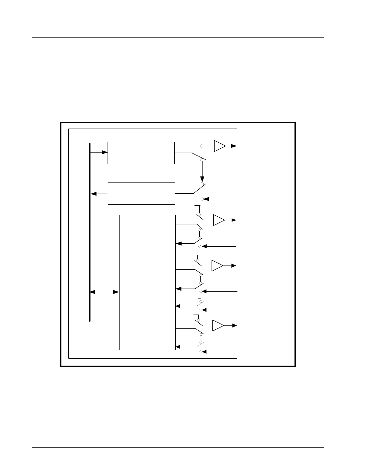
The 2850 UART provides an internal loopback capability for system diagnostic purposes. The internal
loopback mode
is enabled by setting MCR register bit-4 to logic 1. All regular UART functions operate normally.
Figure 13 shows how the modem port signals are re-configured. Transmit data from the transmit shift register
output is internally routed to the receive shift register input allowing the system to receive the same data that it
was sending. The TX pin is held HIGH or mark condition while RTS# and DTR# are de-asserted, and CTS#,
DSR# CD# and RI# inputs are ignored. Caution: the RX input must be held HIGH during loopback test else
upon exiting the loopback test the UART may detect and report a false “break” signal.
FIGURE 13. INTERNAL LOOP BACK IN CHANNELS A AND B
VCC
Transmit Shift Register
(THR/FIFO)
MCR bit-4=1
Receive Shift Register
(RHR/FIFO)
VCC
TXA/TXB
RXA/RXB
RTS#
CTS#
VCC
DTR#
DSR#
Internal Data Bus Lines and Control Signals
RI#
OP2#
Modem / General Purpose Control Logic
CD#
OP1#
VCC
RTSA#/RTSB#
CTSA#/CTSB#
DTRA#/DTRB#
DSRA#/DSRB#
RIA#/RIB#
OP2A#/OP2B#
CDA#/CDB#
20
Page 21
xr XR16C2850
REV. 2.1.3 2.97V TO 5.5V DUAL UART WITH 128-BYTE FIFOS
3.0 UART INTERNAL REGISTERS
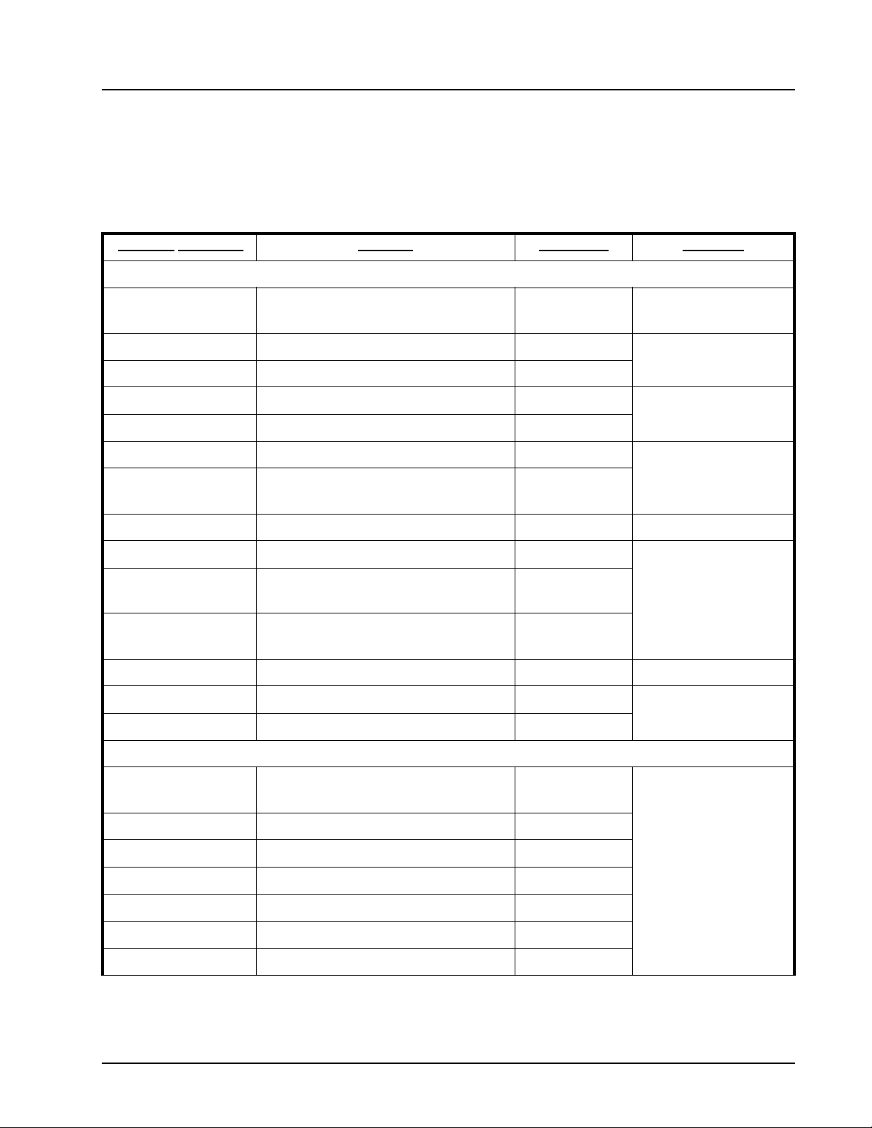
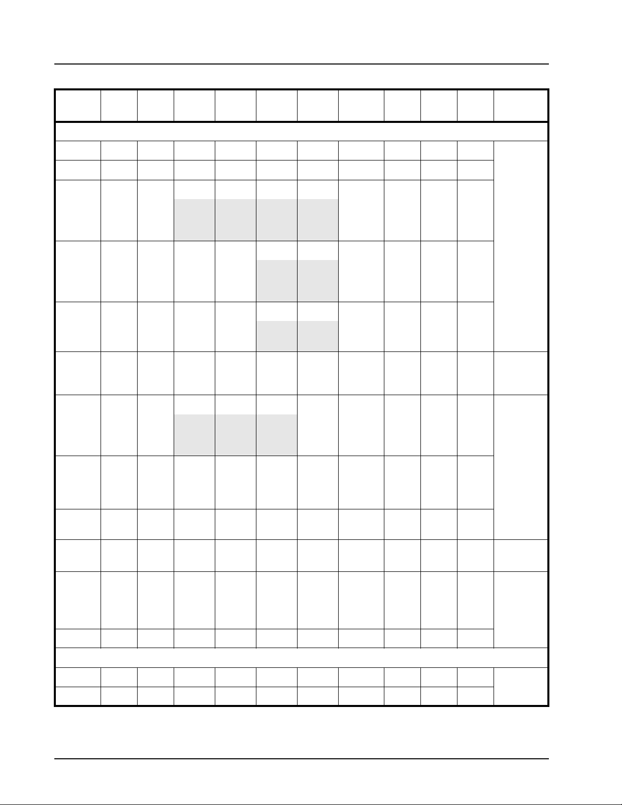
Each of the UART channel in the 2850 has its own set of configuration registers selected by address lines A0,
A1 and A2 with CSA# or CSB# selecting the channel. The complete register set is shown on
Table 8.
.
TABLE 7: UART CHANNEL A AND B UART INTERNAL REGISTERS
A2,A1,A0 ADDRESSES REGISTER READ/WRITE COMMENTS
16C550 COMPATIBLE REGISTERS
Tab le 7 and
0 0 0 RHR - Receive Holding Register
THR - Transmit Holding Register
0 0 0 DLL - Div Latch Low Byte Read/Write
0 0 1 DLM - Div Latch High Byte Read/Write
0 0 0 DREV - Device Revision Code Read-only
0 0 1 DVID - Device Identification Code Read-only
0 0 1 IER - Interrupt Enable Register Read/Write
0 1 0 ISR - Interrupt Status Register
FCR - FIFO Control Register
0 1 1 LCR - Line Control Register Read/Write
1 0 0 MCR - Modem Control Register Read/Write
1 0 1 LSR - Line Status Register
Reserved
1 1 0 MSR - Modem Status Register
Reserved
1 1 1 SPR - Scratch Pad Register Read/Write LCR[7] = 0, FCTR[6] = 0
1 1 1 FLVL - TX/RX FIFO Level Counter Register Read-only
1 1 1 EMSR - Enhanced Mode Select Register Write-only
Read-only
Write-only
Read-only
Write-only
Read-only
Write-only
Read-only
Write-only
LCR[7] = 0
LCR[7] = 1, LCR ≠ 0xBF
DLL, DLM = 0x00,
LCR[7] = 1, LCR ≠ 0xBF
LCR[7] = 0
LCR[7] = 0
LCR[7] = 0, FCTR[6] = 1
ENHANCED REGISTERS
0 0 0 TRG - TX/RX FIFO Trigger Level Reg
FC - TX/RX FIFO Level Counter Register
0 0 1 FCTR - Feature Control Reg Read/Write
0 1 0 EFR - Enhanced Function Reg Read/Write
1 0 0 Xon-1 - Xon Character 1 Read/Write
1 0 1 Xon-2 - Xon Character 2 Read/Write
1 1 0 Xoff-1 - Xoff Character 1 Read/Write
1 1 1 Xoff-2 - Xoff Character 2 Read/Write
Write-only
Read-only
21
LCR = 0xBF
Page 22
XR16C2850 xr
2.97V TO 5.5V DUAL UART WITH 128-BYTE FIFOS REV. 2.1.3
TABLE 8: INTERNAL REGISTERS DESCRIPTION. SHADED BITS ARE ENABLED WHEN EFR BIT-4=1
ADDRESS
A2-A0
0 0 0 RHR RD Bit-7 Bit-6 Bit-5 Bit-4 Bit-3 Bit-2 Bit-1 Bit-0
0 0 0 THR WR Bit-7 Bit-6 Bit-5 Bit-4 Bit-3 Bit-2 Bit-1 Bit-0
0 0 1 IER RD/WR 0/ 0/ 0/ 0/ Modem
0 1 0 ISR RD FIFOs
0 1 0 FCR WR RX FIFO
0 1 1 LCR RD/WR Divisor
REG
NAME
READ/
WRITE
BIT-7 BIT-6 BIT-5 BIT-4 BIT-3 BIT-2 BIT-1 BIT-0 COMMENT
16C550 Compatible Registers
CTS#
Int.
Enable
Enabled
Trigger
Enable
RTS#
Int.
Enable
FIFOs
Enabled
RX FIFO
Trigger
Set TX
Break
Xoff Int..
Enable
0/ 0/ INT
INT
Source
Bit-5
0/ 0/ DMA
TX FIFO
Trigger
Set
Parity
Sleep
Mode
Enable
Source
Bit-4
TX FIFO
Trigger
Even
Parity
Status Int.
INT
Enable
Source
Bit-3
Mode
Enable
Parity
Enable
RX Line
Status
Int.
Enable
INT
Source
Bit-2
TX
FIFO
Reset
Stop
Bits
-
Enable
Source
Length
TX
Empty
Int.
INT
Bit-1
RX
FIFO
Reset
Word
Bit-1
RX
Data
Int.
Enable
INT
Source
Bit-0
FIFOs
Enable
Word
Length
Bit-0
LCR[7] = 0
1 0 0 MCR RD/WR 0/ 0/ 0/ Internal
BRG
Pres
caler
1 0 1 LSR RD RX FIFO
Global
Error
1 1 0 MSR RD CD#
Input
1 1 1 SPR RD/WR Bit-7 Bit-6 Bit-5 Bit-4 Bit-3 Bit-2 Bit-1 Bit-0 LCR[7] = 0
1 1 1 EMSR WR Rsvd Rsvd Auto
1 1 1 FLVL RD Bit-7 Bit-6 Bit-5 Bit-4 Bit-3 Bit-2 Bit-1 Bit-0
0 0 0 DLL RD/WR Bit-7 Bit-6 Bit-5 Bit-4 Bit-3 Bit-2 Bit-1 Bit-0 LCR[7] = 1
0 0 1 DLM RD/WR Bit-7 Bit-6 Bit-5 Bit-4 Bit-3 Bit-2 Bit-1 Bit-0
-
IR Mode
ENable
THR &
TSR
Empty
RI#
Input
XonAny
THR
Empty
DSR#
Input
RTS
Hyst.
bit-3
Baud Rate Generator Divisor
Lopback
Enable
Break
CTS#
Input
Auto
RTS
Hyst.
bit-2
RX
OP2#/INT
Output
Enable
RX Fram-
ing Error
Delta
CD#
Rsvd Rsvd Rx/Tx
Rsvd
(OP1#)
RX
Parity
Error
Delta
RI#
Output
Control
RTS#
RX
Over-
run
Error
Delta
DSR#
FIFO
Count
DTR#
Output
Control
RX
Data
Ready
Delta
CTS#
Rx/Tx
FIFO
Count
LCR[7] = 0
FCTR[6]=0
LCR[7] = 0
FCTR[6]=1
LCR ≠ 0xBF
22
Page 23

xr XR16C2850
REV. 2.1.3 2.97V TO 5.5V DUAL UART WITH 128-BYTE FIFOS
TABLE 8: INTERNAL REGISTERS DESCRIPTION. SHADED BITS ARE ENABLED WHEN EFR BIT-4=1
ADDRESS
A2-A0
0 0 0 DREV RD Bit-7 Bit-6 Bit-5 Bit-4 Bit-3 Bit-2 Bit-1 Bit-0 LCR[7] = 1
0 0 1 DVID RD 0 0 0 1 0 0 1 0
0 0 0 TRG WR Bit-7 Bit-6 Bit-5 Bit-4 Bit-3 Bit-2 Bit-1 Bit-0
0 0 0 FC RD Bit-7 Bit-6 Bit-5 Bit-4 Bit-3 Bit-2 Bit-1 Bit-0
0 0 1 FCTR RD/WR RX/TX
0 1 0 EFR RD/WR Auto
1 0 0 XON1 RD/WR Bit-7 Bit-6 Bit-5 Bit-4 Bit-3 Bit-2 Bit-1 Bit-0
1 0 1 XON2 RD/WR Bit-7 Bit-6 Bit-5 Bit-4 Bit-3 Bit-2 Bit-1 Bit-0
REG
NAME
READ/
WRITE
BIT-7 BIT-6 BIT-5 BIT-4 BIT-3 BIT-2 BIT-1 BIT-0 COMMENT
LCR ≠ 0xBF
DLL=0x00
DLM=0x00
Enhanced Registers
Mode
CTS
Enable
SCPAD
Swap
Auto
RTS
Enable
Trig
Ta bl e
Bit-1
Special
Char
Select
Trig
Ta bl e
Bit-0
Enable
IER [7:4],
ISR [5:4],
FCR[5:4],
MCR[7:5]
Auto
RS485
Direction
Control
Software
Flow
Cntl
Bit-3
RX IR
Input
Inv.
Software
Flow
Cntl
Bit-2
Auto
RTS
Hyst
Bit-1
Software
Flow
Cntl
Bit-1
Auto
RTS
Hyst
Bit-0
Software
Flow
Cntl
Bit-0
LCR=0XBF
1 1 0 XOFF1 RD/WR Bit-7 Bit-6 Bit-5 Bit-4 Bit-3 Bit-2 Bit-1 Bit-0
1 1 1 XOFF2 RD/WR Bit-7 Bit-6 Bit-5 Bit-4 Bit-3 Bit-2 Bit-1 Bit-0
4.0 INTERNAL REGISTER DESCRIPTIONS
4.1 Receive Holding Register (RHR) - Read- Only
SEE”RECEIVER” ON PAGE 14.
4.2 Transmit Holding Register (THR) - Write-Only
SEE”TRANSMITTER” ON PAGE 12.
4.3 Interrupt Enable Register (IER) - Read/Write
The Interrupt Enable Register (IER) masks the interrupts from receive data ready, transmit empty, line status
and modem status registers. These interrupts are reported in the Interrupt Status Register (ISR).
4.3.1 IER versus Receive FIFO Interrupt Mode Operation
When the receive FIFO (FCR BIT-0 = 1) and receive interrupts (IER BIT-0 = 1) are enabled, the RHR interrupts
(see ISR bits 2 and 3) status will reflect the following:
A. The receive data available interrupts are issued to the host when the FIFO has reached the programmed
trigger level. It will be cleared when the FIFO drops below the programmed trigger level.
B. FIFO level will be reflected in the ISR register when the FIFO trigger level is reached. Both the ISR register
status bit and the interrupt will be cleared when the FIFO drops below the trigger level.
C. The receive data ready bit (LSR BIT-0) is set as soon as a character is transferred from the shift register to
the receive FIFO. It is reset when the FIFO is empty.
23
Page 24

XR16C2850 xr
2.97V TO 5.5V DUAL UART WITH 128-BYTE FIFOS REV. 2.1.3
4.3.2 IER versus Receive/Transmit FIFO Polled Mode Operation
When FCR BIT-0 equals a logic 1 for FIFO enable; resetting IER bits 0-3 enables the XR16C2850 in the FIFO
polled mode of operation. Since the receiver and transmitter have separate bits in the LSR either or both can
be used in the polled mode by selecting respective transmit or receive control bit(s).
A. LSR BIT-0 indicates there is data in RHR or RX FIFO.
B. LSR BIT-1 indicates an overrun error has occurred and that data in the FIFO may not be valid.
C. LSR BIT 2-4 provides the type of receive data errors encountered for the data byte in RHR, if any.
D. LSR BIT-5 indicates THR is empty.
E. LSR BIT-6 indicates when both the transmit FIFO and TSR are empty.
F. LSR BIT-7 indicates a data error in at least one character in the RX FIFO.
IER[0]: RHR Interrupt Enable
The receive data ready interrupt will be issued when RHR has a data character in the non-FIFO mode or when
the receive FIFO has reached the programmed trigger level in the FIFO mode.
• Logic 0 = Disable the receive data ready interrupt (default).
• Logic 1 = Enable the receiver data ready interrupt.
IER[1]: THR Interrupt Enable
This bit enables the Transmit Ready interrupt which is issued whenever the THR becomes empty in the nonFIFO mode or when data in the FIFO falls below the programmed trigger level in the FIFO mode. If the THR is
empty when this bit is enabled, an interrupt will be generated.
• Logic 0 = Disable Transmit Ready interrupt (default).
• Logic 1 = Enable Transmit Ready interrupt.
IER[2]: Receive Line Status Interrupt Enable
If any of the LSR register bits 1, 2, 3 or 4 is a logic 1, it will generate an interrupt to inform the host controller
about the error status of the current data byte in FIFO. LSR bits 1-4 generate an interrupt immediately when
the character has been received.
• Logic 0 = Disable the receiver line status interrupt (default).
• Logic 1 = Enable the receiver line status interrupt.
IER[3]: Modem Status Interrupt Enable
• Logic 0 = Disable the modem status register interrupt (default).
• Logic 1 = Enable the modem status register interrupt.
IER[4]: Sleep Mode Enable (requires EFR bit-4 = 1)
• Logic 0 = Disable Sleep Mode (default).
• Logic 1 = Enable Sleep Mode. See Sleep Mode section for complete details.
IER[5]: Xoff Interrupt Enable (requires EFR bit-4=1)
• Logic 0 = Disable the software flow control, receive Xoff interrupt (default).
• Logic 1 = Enable the software flow control, receive Xoff interrupt. See Software Flow Control section for
details.
IER[6]: RTS# Output Interrupt Enable (requires EFR bit-4=1)
• Logic 0 = Disable the RTS# interrupt (default).
• Logic 1 = Enable the RTS# interrupt. The UART issues an interrupt when the RTS# pin makes a transition
from LOW to HIGH.
24
Page 25
xr XR16C2850
REV. 2.1.3 2.97V TO 5.5V DUAL UART WITH 128-BYTE FIFOS
IER[7]: CTS# Input Interrupt Enable (requires EFR bit-4=1)
• Logic 0 = Disable the CTS# interrupt (default).
• Logic 1 = Enable the CTS# interrupt. The UART issues an interrupt when CTS# pin makes a transition from
LOW to HIGH.
4.4 Interrupt Status Register (ISR) - Read-Only
The UART provides multiple levels of prioritized interrupts to minimize external software interaction. The
Interrupt Status Register (ISR) provides the user with six interrupt status bits. Performing a read cycle on the
ISR will give the user the current highest pending interrupt level to be serviced, others are queued up to be
serviced next. No other interrupts are acknowledged until the pending interrupt is serviced. The Interrupt
Source Table,
associated with each of these interrupt levels.
4.4.1 Interrupt Generation:
• LSR is by any of the LSR bits 1, 2, 3 and 4.
• RXRDY is by RX trigger level.
• RXRDY Time-out is by a 4-char plus 12 bits delay timer.
• TXRDY is by TX trigger level or TX FIFO empty (or transmitter empty in auto RS-485 control).
• MSR is by any of the MSR bits 0, 1, 2 and 3.
• Receive Xoff/Special character is by detection of a Xoff or Special character.
• CTS# is when its transmitter toggles the input pin (from LOW to HIGH) during auto CTS flow control enabled
by EFR bit-7.
• RTS# is when its receiver toggles the output pin (from LOW to HIGH) during auto RTS flow control enabled
by EFR bit-6.
4.4.2 Interrupt Clearing:
Tab le 9, shows the data values (bit 0-5) for the interrupt priority levels and the interrupt sources
• LSR interrupt is cleared by a read to the LSR register.
• RXRDY interrupt is cleared by reading data until FIFO falls below the trigger level.
• RXRDY Time-out interrupt is cleared by reading RHR.
• TXRDY interrupt is cleared by a read to the ISR register or writing to THR.
• MSR interrupt is cleared by a read to the MSR register.
• Xoff interrupt is cleared by a read to ISR or when Xon character(s) is received.
• Special character interrupt is cleared by a read to ISR or after the next character is received.
• RTS# and CTS# flow control interrupts are cleared by a read to the MSR register.
]
TABLE 9: INTERRUPT SOURCE AND PRIORITY LEVEL
PRIORITY ISR REGISTER STATUS BITS SOURCE OF INTERRUPT
LEVEL BIT-5 BIT-4 BIT-3 BIT-2 BIT-1 BIT-0
1 0 0 0 1 1 0 LSR (Receiver Line Status Register)
2 0 0 1 1 0 0 RXRDY (Receive Data Time-out)
3 0 0 0 1 0 0 RXRDY (Received Data Ready)
4 0 0 0 0 1 0 TXRDY (Transmit Ready)
5 0 0 0 0 0 0 MSR (Modem Status Register)
6 0 1 0 0 0 0 RXRDY (Received Xoff or Special character)
25
Page 26

XR16C2850 xr
2.97V TO 5.5V DUAL UART WITH 128-BYTE FIFOS REV. 2.1.3
TABLE 9: INTERRUPT SOURCE AND PRIORITY LEVEL
PRIORITY ISR REGISTER STATUS BITS SOURCE OF INTERRUPT
LEVEL BIT-5 BIT-4 BIT-3 BIT-2 BIT-1 BIT-0
7 1 0 0 0 0 0 CTS#, RTS# change of state
- 0 0 0 0 0 1 None (default)
ISR[0]: Interrupt Status
• Logic 0 = An interrupt is pending and the ISR contents may be used as a pointer to the appropriate interrupt
service routine.
• Logic 1 = No interrupt pending (default condition).
ISR[5:1]: Interrupt Status
These bits indicate the source for a pending interrupt at interrupt priority levels (See Table 9). See “Section
4.4.1, Interrupt Generation:” on page 25 and “Section 4.4.2, Interrupt Clearing:” on page 25 for details.
ISR[7:6]: FIFO Enable Status
These bits are set to a logic 0 when the FIFOs are disabled. They are set to a logic 1 when the FIFOs are
enabled.
4.5 FIFO Control Register (FCR) - Write-Only
This register is used to enable the FIFOs, clear the FIFOs, set the transmit/receive FIFO trigger levels, and
select the DMA mode. The DMA, and FIFO modes are defined as follows:
FCR[0]: TX and RX FIFO Enable
• Logic 0 = Disable the transmit and receive FIFO (default).
• Logic 1 = Enable the transmit and receive FIFOs. This bit must be set to logic 1 when other FCR bits are
written or they will not be programmed.
FCR[1]: RX FIFO Reset
This bit is only active when FCR bit-0 is a ‘1’.
• Logic 0 = No receive FIFO reset (default).
• Logic 1 = Reset the receive FIFO pointers and FIFO level counter logic (the receive shift register is not
cleared or altered). This bit will return to a logic 0 after resetting the FIFO.
FCR[2]: TX FIFO Reset
This bit is only active when FCR bit-0 is a ‘1’.
• Logic 0 = No transmit FIFO reset (default).
• Logic 1 = Reset the transmit FIFO pointers and FIFO level counter logic (the transmit shift register is not
cleared or altered). This bit will return to a logic 0 after resetting the FIFO.
26
Page 27

xr XR16C2850
REV. 2.1.3 2.97V TO 5.5V DUAL UART WITH 128-BYTE FIFOS
FCR[3]: DMA Mode Select
Controls the behavior of the TXRDY# and RXRDY# pins. See DMA operation section for details.
• Logic 0 = Normal Operation (default).
• Logic 1 = DMA Mode.
FCR[5:4]: Transmit FIFO Trigger Select
(logic 0 = default, TX trigger level = 1)
These 2 bits set the trigger level for the transmit FIFO. The UART will issue a transmit interrupt when the
number of characters in the FIFO falls below the selected trigger level, or when it gets empty in case that the
FIFO did not get filled over the trigger level on last re-load.
must be set to ‘1’ before these bits can be accessed. Note that the receiver and the transmitter cannot use
different trigger tables. Whichever selection is made last applies to both the RX and TX side.
FCR[7:6]: Receive FIFO Trigger Select
(logic 0 = default, RX trigger level =1)
The FCTR Bits 5-4 are associated with these 2 bits. These 2 bits are used to set the trigger level for the receive
FIFO. The UART will issue a receive interrupt when the number of the characters in the FIFO crosses the
trigger level.
Table 10 shows the complete selections. Note that the receiver and the transmitter cannot use
different trigger tables. Whichever selection is made last applies to both the RX and TX side.
Tab le 10 below shows the selections. EFR bit-4
TABLE 10: TRANSMIT AND RECEIVE FIFO TRIGGER TABLE AND LEVEL SELECTION
TRIGGER
TABLE
Ta bl e- A 0 0
Ta bl e- B 0 1
Table-C 1 0
FCTR
BIT-5
FCTR
BIT-4
FCR
BIT-7
0
0
1
1
0
0
1
1
0
0
1
1
FCR
BIT-6
0
1
0
1
0
1
0
1
0
1
0
1
FCR
BIT-5
0 0
0
0
1
1
0
0
1
1
FCR
BIT-4
0
1
0
1
0
1
0
1
RECEIVE
TRIGGER LEVEL
1 (default)
4
8
14
8
16
24
28
8
16
56
60
TRANSMIT
TRIGGER
EVEL
L
1 (default) 16C550, 16C2550,
16
8
24
30
8
16
32
56
COMPATIBILITY
16C2552, 16C554,
16C580
16C650A
16C654
Table-D 1 1 X X X X Programmable
via TRG
register.
FCTR[7] = 0.
27
Programmable
via TRG
register.
FCTR[7] = 1.
16L2752, 16L2750,
16C2852, 16C850,
16C854, 16C864
Page 28
XR16C2850 xr
2.97V TO 5.5V DUAL UART WITH 128-BYTE FIFOS REV. 2.1.3
4.6 Line Control Register (LCR) - Read/Write
The Line Control Register is used to specify the asynchronous data communication format. The word or
character length, the number of stop bits, and the parity are selected by writing the appropriate bits in this
register.
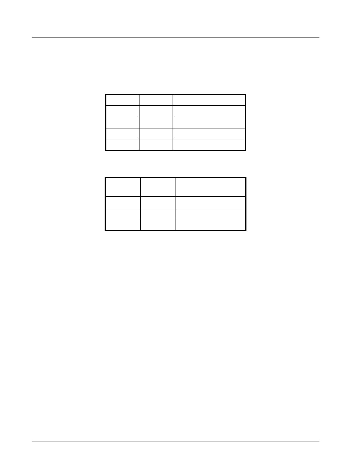
LCR[1:0]: TX and RX Word Length Select
These two bits specify the word length to be transmitted or received.
BIT-1 BIT-0 WORD LENGTH
0 0 5 (default)
0 1 6
1 0 7
1 1 8
LCR[2]: TX and RX Stop-bit Length Select
The length of stop bit is specified by this bit in conjunction with the programmed word length.
BIT-2
0 5,6,7,8 1 (default)
1 5 1-1/2
1 6,7,8 2
WORD
LENGTH
STOP BIT LENGTH
(BIT TIME(S))
LCR[3]: TX and RX Parity Select
Parity or no parity can be selected via this bit. The parity bit is a simple way used in communications for data
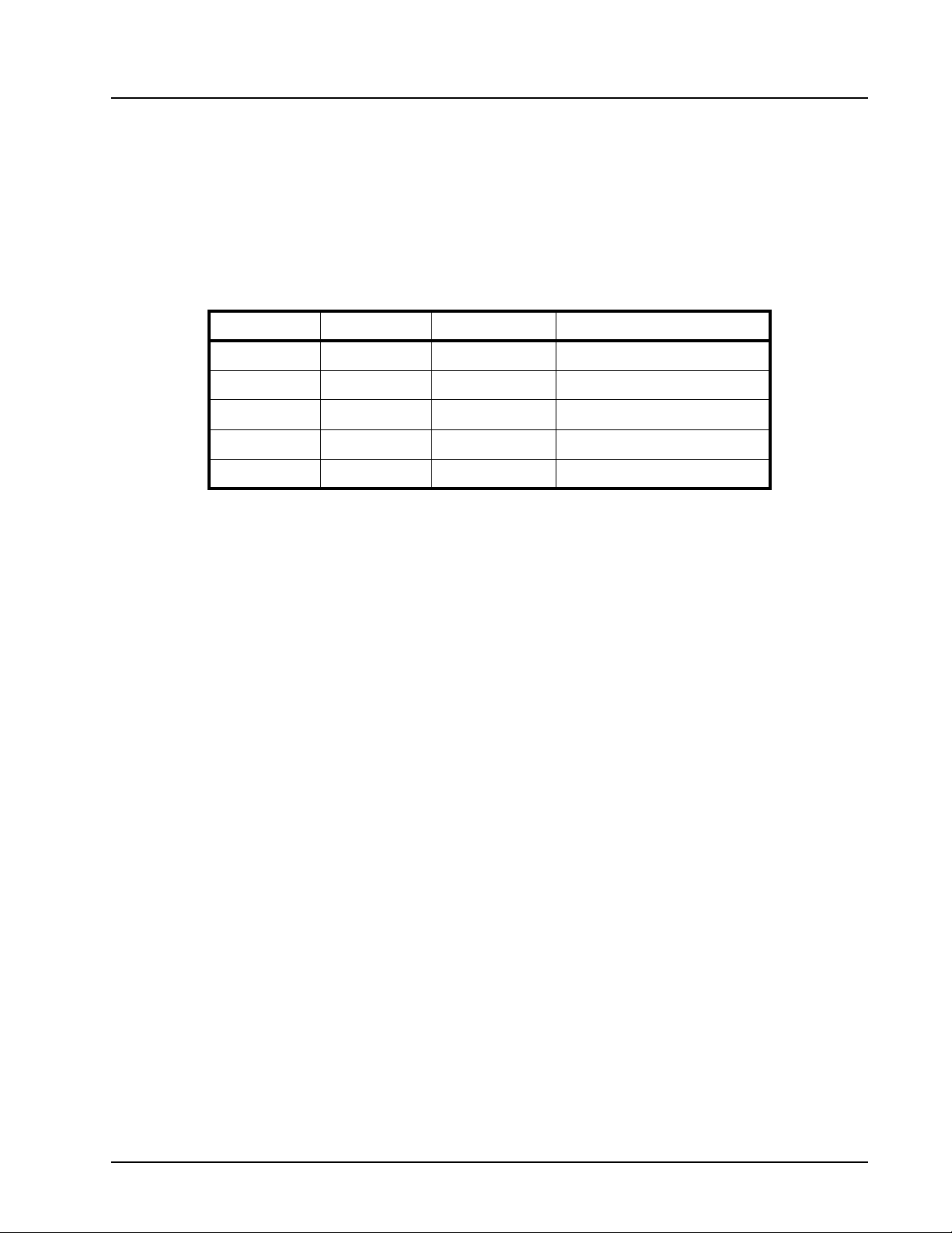
integrity check. See
Table 11 for parity selection summary below.
• Logic 0 = No parity.
• Logic 1 = A parity bit is generated during the transmission while the receiver checks for parity error of the
data character received.
LCR[4]: TX and RX Parity Select
If the parity bit is enabled with LCR bit-3 set to a logic 1, LCR BIT-4 selects the even or odd parity format.
• Logic 0 = ODD Parity is generated by forcing an odd number of logic 1’s in the transmitted character. The
receiver must be programmed to check the same format (default).
• Logic 1 = EVEN Parity is generated by forcing an even number of logic 1’s in the transmitted character. The
receiver must be programmed to check the same format.
28
Page 29
xr XR16C2850
REV. 2.1.3 2.97V TO 5.5V DUAL UART WITH 128-BYTE FIFOS
LCR[5]: TX and RX Parity Select
If the parity bit is enabled, LCR BIT-5 selects the forced parity format.
• LCR BIT-5 = logic 0, parity is not forced (default).
• LCR BIT-5 = logic 1 and LCR BIT-4 = logic 0, parity bit is forced to a logical 1 for the transmit and receive
data.
• LCR BIT-5 = logic 1 and LCR BIT-4 = logic 1, parity bit is forced to a logical 0 for the transmit and receive
data.
TABLE 11: PARITY SELECTION
LCR BIT-5 LCR BIT-4 LCR BIT-3 PARITY SELECTION
X X 0 No parity
0 0 1 Odd parity
0 1 1 Even parity
1 0 1 Force parity to mark, “1”
1 1 1 Forced parity to space, “0”
LCR[6]: Transmit Break Enable
When enabled, the Break control bit causes a break condition to be transmitted (the TX output is forced to a
“space’, LOW, state). This condition remains, until disabled by setting LCR bit-6 to a logic 0.
• Logic 0 = No TX break condition (default).
• Logic 1 = Forces the transmitter output (TX) to a “space”, LOW, for alerting the remote receiver of a line
break condition.
LCR[7]: Baud Rate Divisors Enable
Baud rate generator divisor (DLL/DLM) enable.
• Logic 0 = Data registers are selected (default).
• Logic 1 = Divisor latch registers are selected.
4.7 Modem Control Register (MCR) or General Purpose Outputs Control - Read/Write
The MCR register is used for controlling the serial/modem interface signals or general purpose inputs/outputs.
MCR[0]: DTR# Output
The DTR# pin is a modem control output. If the modem interface is not used, this output may be used as a
general purpose output.
• Logic 0 = Force DTR# output HIGH (default).
• Logic 1 = Force DTR# output LOW.
MCR[1]: RTS# Output
The RTS# pin is a modem control output and may be used for automatic hardware flow control enabled by
EFR bit-6. The RTS# output must be asserted before the auto RTS can take effect. If the modem interface is
not used, this output may be used as a general purpose output.
• Logic 0 = Force RTS# output HIGH (default).
• Logic 1 = Force RTS# output LOW. If auto RTS flow control is enabled, it will take effect after this bit has
been set.
MCR[2]: Reserved
OP1# is not available as an output pin on the 2850. But it is available for use during Internal Loopback Mode.
In the Loopback Mode, this bit is used to write the state of the modem RI# interface signal.
29
Page 30

XR16C2850 xr
2.97V TO 5.5V DUAL UART WITH 128-BYTE FIFOS REV. 2.1.3
MCR[3]: OP2# Output / INT Output Enable
This bit enables and disables the operation of INT, interrupt output. If INT output is not used, OP2# can be
used as a general purpose output.
• Logic 0 = INT (A-B) outputs disabled (three state mode) and OP2# output is HIGH (default).
• Logic 1 = INT (A-B) outputs enabled (active mode) and OP2# output is LOW.
MCR[4]: Internal Loopback Enable
• Logic 0 = Disable loopback mode (default).
• Logic 1 = Enable local loopback mode, see loopback section and Figure 13.
MCR[5]: Xon-Any Enable
• Logic 0 = Disable Xon-Any function (for 16C550 compatibility, default).
• Logic 1 = Enable Xon-Any function. In this mode, any RX character received will resume transmit operation.
The RX character will be loaded into the RX FIFO , unless the RX character is an Xon or Xoff character and
the 2850 is programmed to use the Xon/Xoff flow control.
MCR[6]: Infrared Encoder/Decoder Enable
• Logic 0 = Enable the standard modem receive and transmit input/output interface (default).
• Logic 1 = Enable infrared IrDA receive and transmit inputs/outputs. The TX/RX output/input are routed to the
infrared encoder/decoder. The data input and output levels conform to the IrDA infrared interface
requirement. While in this mode, the infrared TX output will be LOW during idle data conditions.
MCR[7]: Clock Prescaler Select
• Logic 0 = Divide by one. The input clock from the crystal or external clock is fed directly to the Programmable
Baud Rate Generator without further modification, i.e., divide by one (default).
• Logic 1 = Divide by four. The prescaler divides the input clock from the crystal or external clock by four and
feeds it to the Programmable Baud Rate Generator, hence, data rates become one forth.
4.8 Line Status Register (LSR) - Read Only
This register provides the status of data transfers between the UART and the host. If IER bit-2 is set to a logic
1, an LSR interrupt will be generated immediately when any character in the RX FIFO has an error (parity,
framing, overrun, break).
LSR[0]: Receive Data Ready Indicator
• Logic 0 = No data in receive holding register or FIFO (default).
• Logic 1 = Data has been received and is saved in the receive holding register or FIFO.
LSR[1]: Receiver Overrun Error Flag
• Logic 0 = No overrun error (default).
• Logic 1 = Overrun error. A data overrun error condition occurred in the receive shift register. This happens
when additional data arrives while the FIFO is full. In this case the previous data in the receive shift register
is overwritten. Note that under this condition the data byte in the receive shift register is not transferred into
the FIFO, therefore the data in the FIFO is not corrupted by the error. If IER bit-2 is set, an interrupt will be
generated immediately.
LSR[2]: Receive Data Parity Error Tag
• Logic 0 = No parity error (default).
• Logic 1 = Parity error. The receive character in RHR does not have correct parity information and is suspect.
This error is associated with the character available for reading in RHR.
30
Page 31

xr XR16C2850
REV. 2.1.3 2.97V TO 5.5V DUAL UART WITH 128-BYTE FIFOS
LSR[3]: Receive Data Framing Error Tag
• Logic 0 = No framing error (default).
• Logic 1 = Framing error. The receive character did not have a valid stop bit(s). This error is associated with
the character available for reading in RHR.
LSR[4]: Receive Break Error Tag
• Logic 0 = No break condition (default).
• Logic 1 = The receiver received a break signal (RX was a logic 0 for at least one character frame time). In the
FIFO mode, only one break character is loaded into the FIFO. The break indication remains until the RX
input returns to the idle condition, “mark” or HIGH.
LSR[5]: Transmit Holding Register Empty Flag
This bit is the Transmit Holding Register Empty indicator. The THR bit is set to a logic 1 when the last data byte
is transferred from the transmit holding register to the transmit shift register. The bit is reset to logic 0
concurrently with the data loading to the transmit holding register by the host. In the FIFO mode this bit is set
when the transmit FIFO is empty, it is cleared when the transmit FIFO contains at least 1 byte.
LSR[6]: THR and TSR Empty Flag
This bit is set to a logic 1 whenever the transmitter goes idle. It is set to logic 0 whenever either the THR or
TSR contains a data character. In the FIFO mode this bit is set to a logic 1 whenever the transmit FIFO and
transmit shift register are both empty.
LSR[7]: Receive FIFO Data Error Flag
• Logic 0 = No FIFO error (default).
• Logic 1 = A global indicator for the sum of all error bits in the RX FIFO. At least one parity error, framing error
or break indication is in the FIFO data. This bit clears when there is no more error(s) in any of the bytes in the
RX FIFO.
4.9 Modem Status Register (MSR) - Read Only
This register provides the current state of the modem interface input signals. Lower four bits of this register are
used to indicate the changed information. These bits are set to a logic 1 whenever a signal from the modem
changes state. These bits may be used for general purpose inputs when they are not used with modem
signals.
MSR[0]: Delta CTS# Input Flag
• Logic 0 = No change on CTS# input (default).
• Logic 1 = The CTS# input has changed state since the last time it was monitored. A modem status interrupt
will be generated if MSR interrupt is enabled (IER bit-3).
MSR[1]: Delta DSR# Input Flag
• Logic 0 = No change on DSR# input (default).
• Logic 1 = The DSR# input has changed state since the last time it was monitored. A modem status interrupt
will be generated if MSR interrupt is enabled (IER bit-3).
MSR[2]: Delta RI# Input Flag
• Logic 0 = No change on RI# input (default).
• Logic 1 = The RI# input has changed from a logic 0 to a logic 1, ending of the ringing signal. A modem status
interrupt will be generated if MSR interrupt is enabled (IER bit-3).
MSR[3]: Delta CD# Input Flag
• Logic 0 = No change on CD# input (default).
• Logic 1 = Indicates that the CD# input has changed state since the last time it was monitored. A modem
status interrupt will be generated if MSR interrupt is enabled (IER bit-3).
31
Page 32

XR16C2850 xr
2.97V TO 5.5V DUAL UART WITH 128-BYTE FIFOS REV. 2.1.3
MSR[4]: CTS Input Status
CTS# pin may function as automatic hardware flow control signal input if it is enabled and selected by Auto
CTS (EFR bit-7). Auto CTS flow control allows starting and stopping of local data transmissions based on the
modem CTS# signal. A HIGH on the CTS# pin will stop UART transmitter as soon as the current character has
finished transmission, and a LOW will resume data transmission. Normally MSR bit-4 bit is the complement of
the CTS# input. However in the loopback mode, this bit is equivalent to the RTS# bit in the MCR register. The
CTS# input may be used as a general purpose input when the modem interface is not used.
MSR[5]: DSR Input Status
Normally this bit is the complement of the DSR# input. In the loopback mode, this bit is equivalent to the DTR#
bit in the MCR register. The DSR# input may be used as a general purpose input when the modem interface is
not used.
MSR[6]: RI Input Status
Normally this bit is the complement of the RI# input. In the loopback mode this bit is equivalent to bit-2 in the
MCR register. The RI# input may be used as a general purpose input when the modem interface is not used.
MSR[7]: CD Input Status
Normally this bit is the complement of the CD# input. In the loopback mode this bit is equivalent to bit-3 in the
MCR register. The CD# input may be used as a general purpose input when the modem interface is not used.
4.10 Scratch Pad Register (SPR) - Read/Write
This is a 8-bit general purpose register for the user to store temporary data. The content of this register is
preserved during sleep mode but becomes 0xFF (default) after a reset or a power off-on cycle.
4.11 Enhanced Mode Select Register (EMSR)
This register replaces SPR (during a Write) and is accessible only when FCTR[6] = 1.
EMSR[1:0]: Receive/Transmit FIFO Count (Write-Only)
When Scratchpad Swap (FCTR[6]) is asserted, EMSR bits 1-0 controls what mode the FIFO Level Counter is
operating in.
TABLE 12: SCRATCHPAD SWAP SELECTION
FCTR[6] EMSR[1] EMSR[0] Scratchpad is
0 X X Scratchpad
1 0 0 RX FIFO Counter Mode
1 0 1 TX FIFO Counter Mode
1 1 0 RX FIFO Counter Mode
1 1 1 Alternate RX/TX FIFO
Counter Mode
During Alternate RX/TX FIFO Counter Mode, the first value read after EMSR bits 1-0 have been asserted will
always be the RX FIFO Counter. The second value read will correspond with the TX FIFO Counter. The next
value will be the RX FIFO Counter again, then the TX FIFO Counter and so on and so forth.
EMSR[3:2]: Reserved
32
Page 33
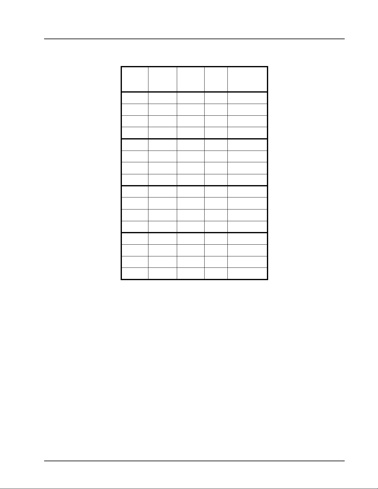
xr XR16C2850
REV. 2.1.3 2.97V TO 5.5V DUAL UART WITH 128-BYTE FIFOS
EMSR[5:4]: Extended RTS Hysteresis
TABLE 13: EXTENDED RTS HYSTERESIS
EMSR
BIT-5
0 0 0 0 0
0 0 0 1 ±4
0 0 1 0 ±6
0 0 1 1 ±8
0 1 0 0 ±8
0 1 0 1 ±16
0 1 1 0 ±24
0 1 1 1 ±32
1 0 0 0 ±40
1 0 0 1 ±44
1 0 1 0 ±48
1 0 1 1 ±52
1 1 0 0 ±12
1 1 0 1 ±20
EMSR
BIT-4
FCTR
BIT-1
FCTR
BIT-0
HYSTERESIS
(C
RTS#
HARACTERS)
1 1 1 0 ±28
1 1 1 1 ±36
EMSR[7:6]: Reserved
4.12 FIFO Level Register (FLVL) - Read-Only
The FIFO Level Register replaces the Scratchpad Register (during a Read) when FCTR[6] = 1. Note that this
is not identical to the FIFO Data Count Register which can be accessed when LCR = 0xBF.
FLVL[7:0]: FIFO Level Register
This register provides the FIFO counter level for the RX FIFO or the TX FIFO or both depending on EMSR[1:0].
See Table 12 for details.
4.13 Baud Rate Generator Registers (DLL and DLM) - Read/Write
The concatenation of the contents of DLM and DLL gives the 16-bit divisor value which is used to calculate the
baud rate:
• Baud Rate = (Clock Frequency / 16) / Divisor
See MCR bit-7 and the baud rate table also.
4.14 Device Identification Register (DVID) - Read Only
This register contains the device ID (0x12 for XR16C2850). Prior to reading this register, DLL and DLM should
be set to 0x00.
4.15 Device Revision Register (DREV) - Read Only
This register contains the device revision information. For example, 0x01 means revision A. Prior to reading
this register, DLL and DLM should be set to 0x00.
33
Page 34
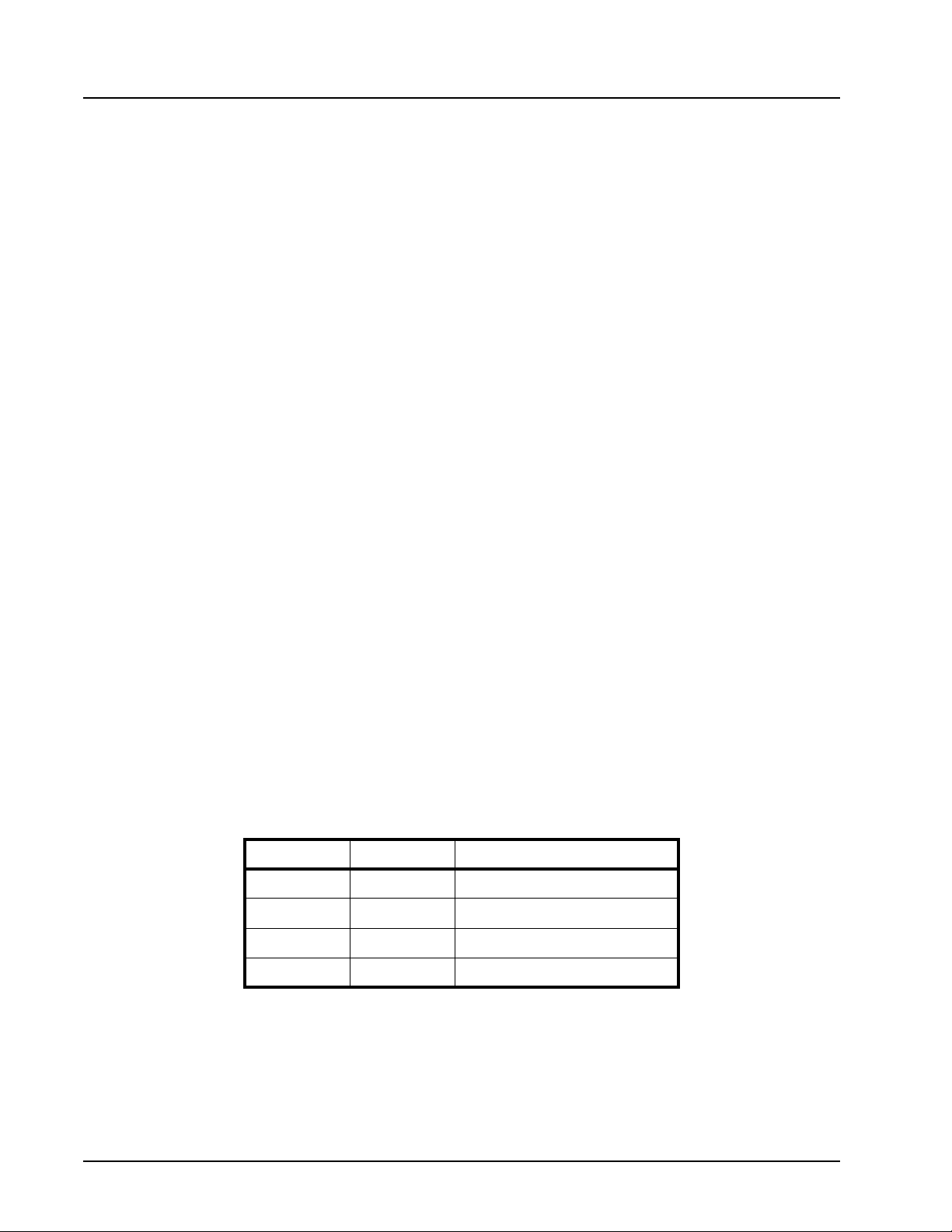
XR16C2850 xr
2.97V TO 5.5V DUAL UART WITH 128-BYTE FIFOS REV. 2.1.3
4.16 Trigger Level / FIFO Data Count Register (TRG) - Write-Only
User Programmable Transmit/Receive Trigger Level Register.
TRG[7:0]: Trigger Level Register
These bits are used to program desired trigger levels when trigger Table-D is selected. FCTR bit-7 selects
between programming the RX Trigger Level (a logic 0) and the TX Trigger Level (a logic 1).
4.17 FIFO Data Count Register (FC) - Read-Only
This register is accessible when LCR = 0xBF. Note that this register is not identical to the FIFO Level Register
which is located in the general register set when FCTR bit-6 = 1.
FC[7:0]: FIFO Data Count Register
Transmit/Receive FIFO Count. Number of characters in Transmit (FCTR[7] = 1) or Receive FIFO (FCTR[7] =
0) can be read via this register.
4.18 Feature Control Register (FCTR) - Read/Write
This register controls the XR16C2850 new functions that are not available in ST16C550 or ST16C650A.
FCTR[1:0]: RTS Hysteresis
User selectable RTS# hysteresis levels for hardware flow control application. After reset, these bits are set to
“0” to select the next trigger level for hardware flow control. See
FCTR[2]: IrDa RX Inversion
Ta bl e 13 for more details.
• Logic 0 = Select RX input as encoded IrDa data (Idle state will be LOW).
• Logic 1 = Select RX input as inverted encoded IrDa data (Idle state will be HIGH).
FCTR[3]: Auto RS-485 Direction Control
This bit controls the functionality of the RTS# output if HDCNTL# is connected to VCC. If HDCNTL# is
connected to GND, then the RTS# output will function as the RS-485 half-duplex direction control signal.
• Logic 0 = Standard ST16C550 mode. Transmitter generates an interrupt when transmit holding register
becomes empty and transmit shift register is shifting data out.
• Logic 1 = Enable Auto RS485 Direction Control function. The direction control signal, RTS# pin, changes its
output logic state from low to high one bit time after the last stop bit of the last character is shifted out. Also,
the Transmit interrupt generation is delayed until the transmitter shift register becomes empty. The RTS#
output pin will automatically return to a logic low when a data byte is loaded into the TX FIFO.
FCTR[5:4]: Transmit/Receive Trigger Table Select
See Tab le 10 for more details.
TABLE 14: TRIGGER TABLE SELECT
FCTR BIT-5 FCTR BIT-4 TABLE
0 0 Table-A (TX/RX)
0 1 Table-B (TX/RX)
1 0 Table-C (TX/RX)
1 1 Table-D (TX/RX)
FCTR[6]: Scratchpad Swap
• Logic 0 = Scratch Pad register is selected as general read and write register. ST16C550 compatible mode.
• Logic 1 = FIFO Count register (Read-Only), Enhanced Mode Select Register (Write-Only). Number of
characters in transmit or receive FIFO can be read via scratch pad register when this bit is set. Enhanced
Mode Select Register is selected when it is written into.
34
Page 35
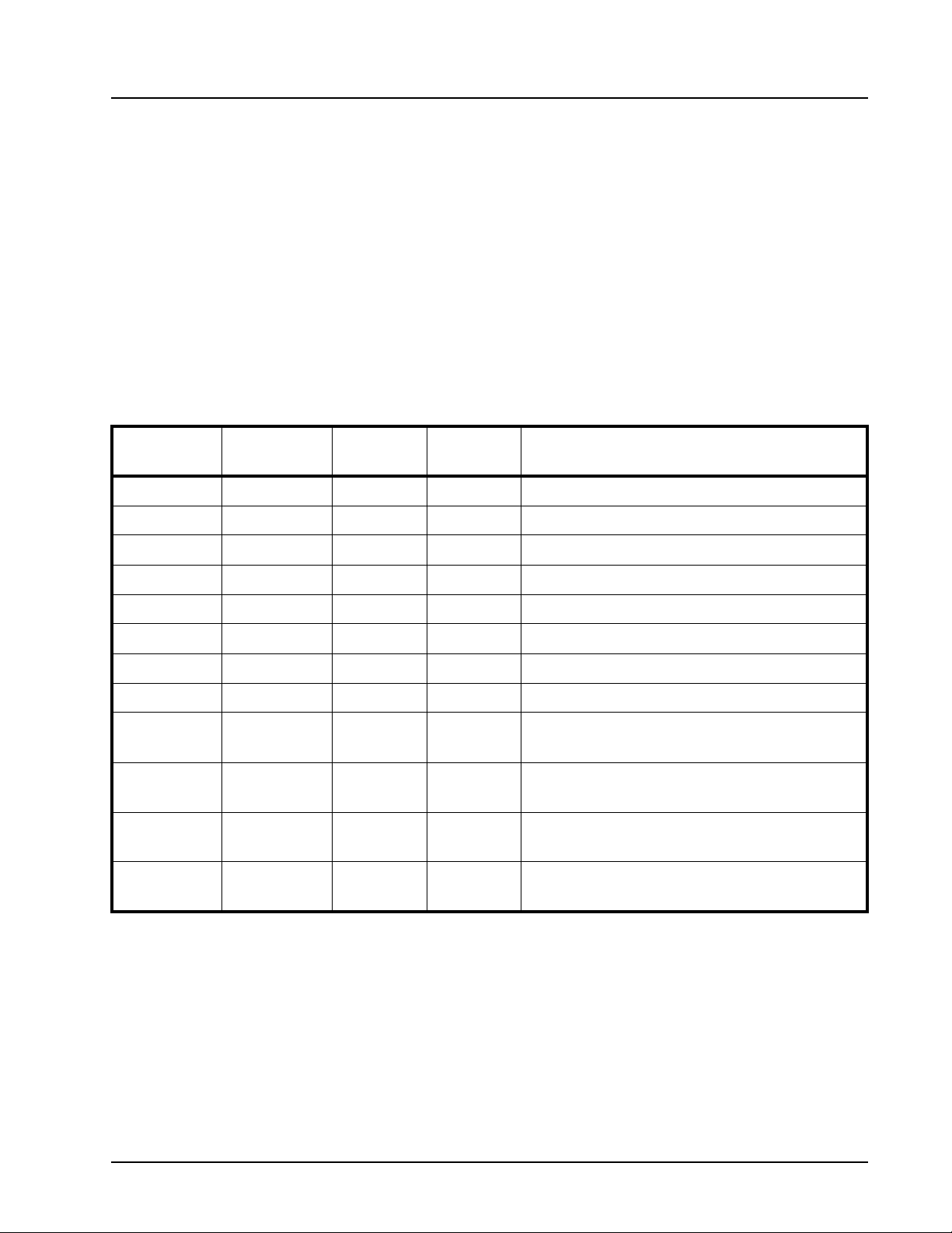
xr XR16C2850
REV. 2.1.3 2.97V TO 5.5V DUAL UART WITH 128-BYTE FIFOS
FCTR[7]: Programmable Trigger Register Select
• Logic 0 = Registers TRG and FC selected for RX.
• Logic 1 = Registers TRG and FC selected for TX.
4.19 Enhanced Feature Register (EFR)
Enhanced features are enabled or disabled using this register. Bit 0-3 provide single or dual consecutive
character software flow control selection (see
are selected, the double 8-bit words are concatenated into two sequential characters. Caution: note that
whenever changing the TX or RX flow control bits, always reset all bits back to logic 0 (disable) before
programming a new setting.
EFR[3:0]: Software Flow Control Select
Single character and dual sequential characters software flow control is supported. Combinations of software
flow control can be selected by programming these bits.
TABLE 15: SOFTWARE FLOW CONTROL FUNCTIONS
Table 15). When the Xon1 and Xon2 and Xoff1 and Xoff2 modes
EFR BIT-3
CONT-3
0 0 0 0 No TX and RX flow control (default and reset)
0 0 X X No transmit flow control
1 0 X X Transmit Xon1, Xoff1
0 1 X X Transmit Xon2, Xoff2
1 1 X X Transmit Xon1 and Xon2, Xoff1 and Xoff2
X X 0 0 No receive flow control
X X 1 0 Receiver compares Xon1, Xoff1
X X 0 1 Receiver compares Xon2, Xoff2
1 0 1 1 Transmit Xon1, Xoff1
0 1 1 1 Transmit Xon2, Xoff2
1 1 1 1 Transmit Xon1 and Xon2, Xoff1 and Xoff2,
0 0 1 1 No transmit flow control,
EFR BIT-2
CONT-2
EFR BIT-1
CONT-1
EFR BIT-0
CONT-0
TRANSMIT AND RECEIVE SOFTWARE FLOW CONTROL
Receiver compares Xon1 or Xon2, Xoff1 or Xoff2
Receiver compares Xon1 or Xon2, Xoff1 or Xoff2
Receiver compares Xon1 and Xon2, Xoff1 and Xoff2
Receiver compares Xon1 and Xon2, Xoff1 and Xoff2
EFR[4]: Enhanced Function Bits Enable
Enhanced function control bit. This bit enables IER bits 4-7, ISR bits 4-5, FCR bits 4-5, and MCR bits 5-7 to be
modified. After modifying any enhanced bits, EFR bit-4 can be set to a logic 0 to latch the new values. This
feature prevents legacy software from altering or overwriting the enhanced functions once set. Normally, it is
recommended to leave it enabled, logic 1.
• Logic 0 = modification disable/latch enhanced features. IER bits 4-7, ISR bits 4-5, FCR bits 4-5, and MCR
bits 5-7 are saved to retain the user settings. After a reset, the IER bits 4-7, ISR bits 4-5, FCR bits 4-5, and
MCR bits 5-7are set to a logic 0 to be compatible with ST16C550 mode (default).
• Logic 1 = Enables the above-mentioned register bits to be modified by the user.
35
Page 36

XR16C2850 xr
2.97V TO 5.5V DUAL UART WITH 128-BYTE FIFOS REV. 2.1.3
EFR[5]: Special Character Detect Enable
• Logic 0 = Special Character Detect Disabled (default).
• Logic 1 = Special Character Detect Enabled. The UART compares each incoming receive character with
data in Xoff-2 register. If a match exists, the receive data will be transferred to FIFO and ISR bit-4 will be set
to indicate detection of the special character. Bit-0 corresponds with the LSB bit of the receive character. If
flow control is set for comparing Xon1, Xoff1 (EFR [1:0]= ‘10’) then flow control
normally. However, if flow control is set for comparing Xon2, Xoff2 (EFR[1:0]= ‘01’) then flow control works
normally, but Xoff2 will
interrupt, if enabled via IER bit-5.
EFR[6]: Auto RTS Flow Control Enable
RTS# output may be used for hardware flow control by setting EFR bit-6 to logic 1. When Auto RTS is
selected, an interrupt will be generated when the receive FIFO is filled to the programmed trigger level and
RTS de-asserts to a logic 1 at the next upper trigger level or hysteresis level. RTS# will return to a logic 0 when
FIFO data falls below the next lower trigger level. The RTS# output must be asserted (logic 0) before the auto
RTS can take effect. RTS# pin will function as a general purpose output when hardware flow control is
disabled.
not go to the FIFO, and will generate an Xoff interrupt and a special character
and special character work
• Logic 0 = Automatic RTS flow control is disabled (default).
• Logic 1 = Enable Automatic RTS flow control.
EFR[7]: Auto CTS Flow Control Enable
Automatic CTS Flow Control.
• Logic 0 = Automatic CTS flow control is disabled (default).
• Logic 1 = Enable Automatic CTS flow control. Data transmission stops when CTS# input de-asserts to logic
1. Data transmission resumes when CTS# returns to a logic 0.
4.20 Software Flow Control Registers (XOFF1, XOFF2, XON1, XON2) - Read/Write
These registers are used as the programmable software flow control characters xoff1, xoff2, xon1, and xon2.
For more details, see
Tab le 6.
36
Page 37
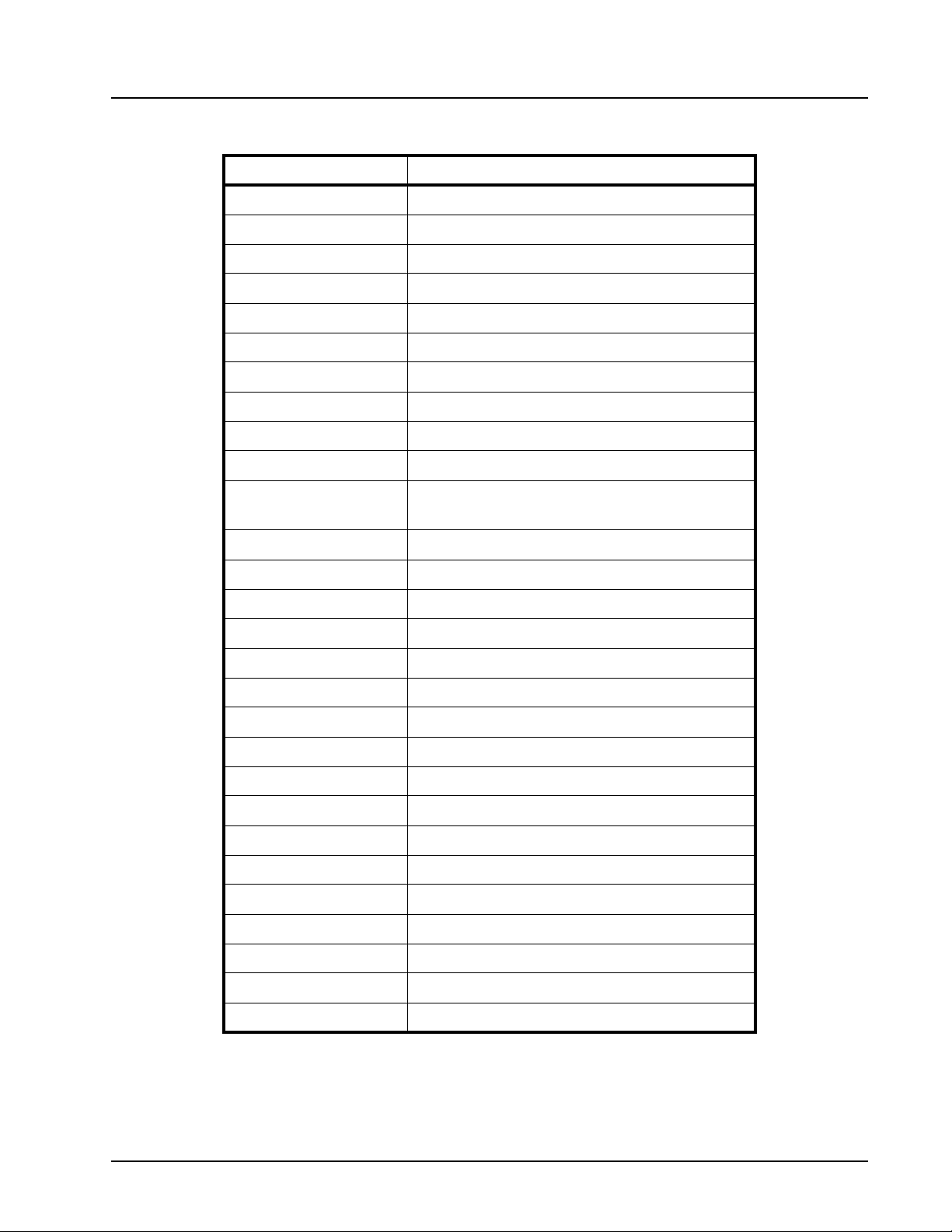
xr XR16C2850
REV. 2.1.3 2.97V TO 5.5V DUAL UART WITH 128-BYTE FIFOS
TABLE 16: UART RESET CONDITIONS FOR CHANNEL A AND B
REGISTERS RESET STATE
DLL Bits 7-0 = 0xXX
DLM Bits 7-0 = 0xXX
RHR Bits 7-0 = 0xXX
THR Bits 7-0 = 0xXX
IER Bits 7-0 = 0x00
FCR Bits 7-0 = 0x00
ISR Bits 7-0 = 0x01
LCR Bits 7-0 = 0x00
MCR Bits 7-0 = 0x00
LSR Bits 7-0 = 0x60
MSR Bits 3-0 = Logic 0
Bits 7-4 = Logic levels of the inputs inverted
SPR Bits 7-0 = 0xFF
EMSR Bits 7-0 = 0x00
FLVL Bits 7-0 = 0x00
EFR Bits 7-0 = 0x00
XON1 Bits 7-0 = 0x00
XON2 Bits 7-0 = 0x00
XOFF1 Bits 7-0 = 0x00
XOFF2 Bits 7-0 = 0x00
FC Bits 7-0 = 0x00
I/O SIGNALS RESET STATE
TX HIGH
OP2# HIGH
RTS# HIGH
DTR# HIGH
RXRDY# HIGH
TXRDY# LOW
INT Three-State Condition
37
Page 38
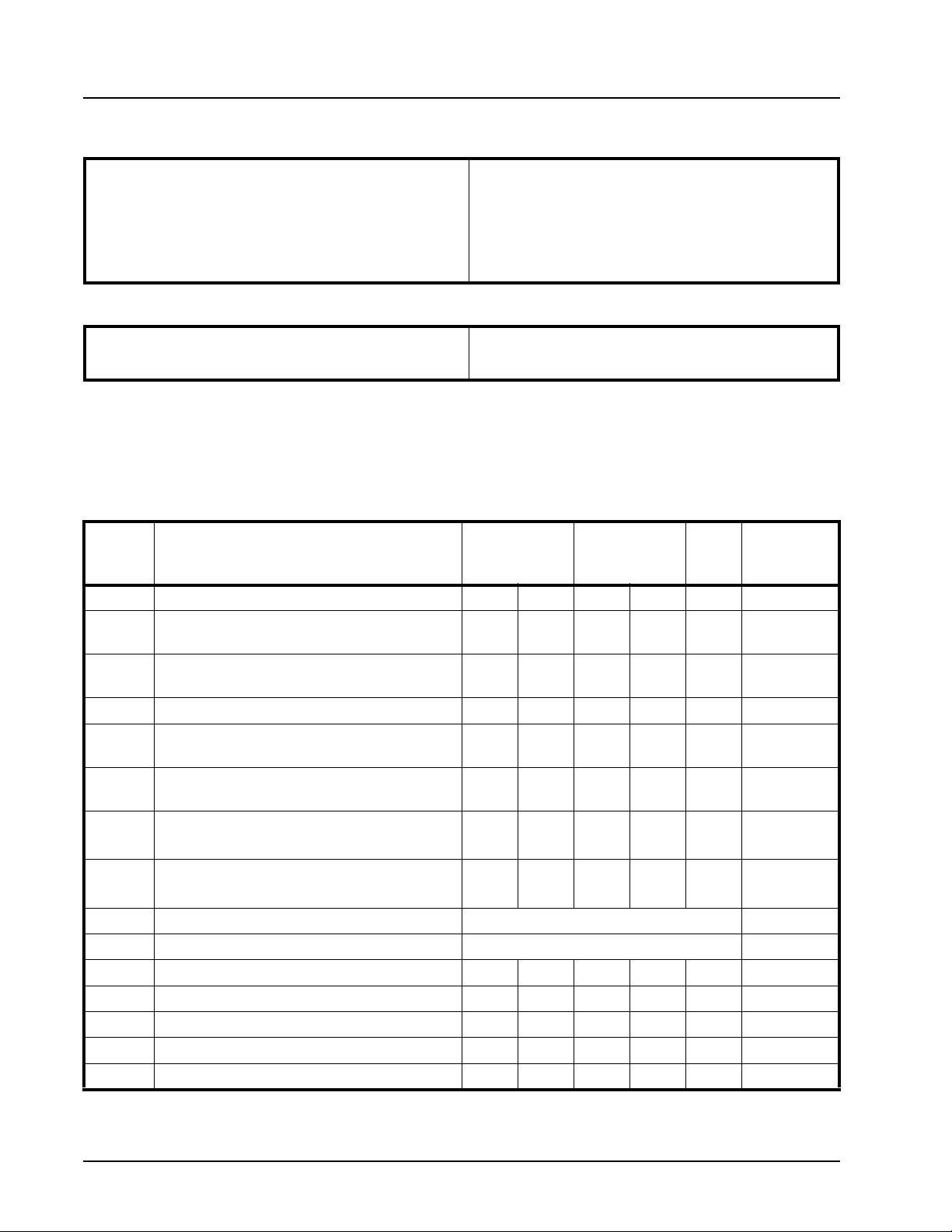
XR16C2850 xr
2.97V TO 5.5V DUAL UART WITH 128-BYTE FIFOS REV. 2.1.3
ABSOLUTE MAXIMUM RATINGS
Power Supply Range 7 Volts
Voltage at Any Pin GND-0.3 V to 7 V
Operating Temperature
Storage Temperature
-40o to +85oC
-65o to +150oC
Package Dissipation 500 mW
TYPICAL PACKAGE THERMAL RESISTANCE DATA (MARGIN OF ERROR: ± 15%)
Thermal Resistance (48-TQFP)
Thermal Resistance (44-PLCC)
ELECTRICAL CHARACTERISTICS
DC ELECTRICAL CHARACTERISTICS
O
UNLESS OTHERWISE NOTED: TA=0
TO 5.5V
SYMBOL PARAMETER
V
ILCK
V
IHCK
V
IHCK
V
V
V
V
OLCK
V
OHCK
V
V
I
I
C
I
CC
I
SLEEP
Clock Input Low Level -0.3 0.6 -0.5 0.6 V
Clock Input High Level
(top mark date code of "DC YYWW" and older)
Clock Input High Level
(top mark date code of "F2 YYWW" and newer)
Input Low Voltage -0.3 0.8 -0.5 0.8 V
IL
Input High Voltage
IH
(top mark date code of "DC YYWW" and older)
Input High Voltage
IH
(top mark date code of "F2 YYWW" and newer)
Clock Output (XTAL2) Low Voltage
Clock Output (XTAL2) High Voltage
Output Low Voltage
OL
Output High Voltage
OH
Input Low Leakage Current ±10 ±10 uA
IL
Input High Leakage Current ±10 ±10 uA
IH
Input Pin Capacitance 5 5 pF
IN
Power Supply Current 1.2 3 mA
Sleep Current 30 100 uA See Test 1
TO
70OC (-40O TO +85OC FOR INDUSTRIAL GRADE PACKAGE), VCC IS 2.97V
theta-ja =59oC/W, theta-jc = 16oC/W
theta-ja = 50oC/W, theta-jc = 21oC/W
LIMITS
3.3V
MIN MAX
LIMITS
5.0V
MIN MAX
UNITS CONDITIONS
2.4 VCC 3.0 VCC V
2.4 5.5 3.0 5.5 V
2.0 VCC 2.2 VCC V
2.0 5.5 2.0 5.5 V
0.4 V IOL = 6 mA
0.4
2.4 V IOH = -6 mA
2.0
See Figure 14.
See Figure 15.
IOL = 4 mA
IOH = -1 mA
Test 1: The following inputs should remain steady at VCC or GND state to minimize Sleep current: A0-A2, D0-D7, IOR#,
IOW#, CSA# and CSB#. Also, RXA and RXB inputs must idle at logic 1 state while asleep.
38
Page 39
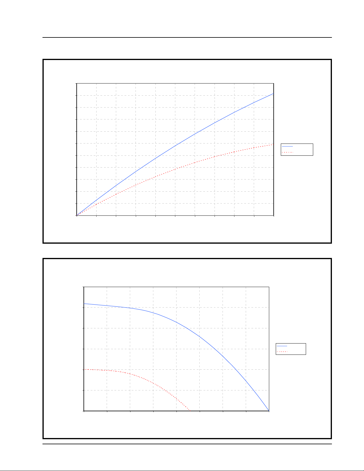
xr XR16C2850
REV. 2.1.3 2.97V TO 5.5V DUAL UART WITH 128-BYTE FIFOS
..
FIGURE 14. XR16C2850 VOL SINK CURRENT CHART
XR16C2850 Sink Current
22
20
18
16
14
12
10
IOL (mA)
8
6
4
2
0
0.00 0.10 0.20 0.30 0.40 0.50 0.60 0.70 0 .80 0.90 1.00
VOL (V)
FIGURE 15. XR16C2850 VOH SOURCE CURRENT CHART
XR16C2850 Source Current
12
10
VCC=5V
VCC=3.3V
8
6
IOH (mA)
4
2
0
1.00 1.50 2.00 2.50 3.00 3.50 4.00 4.50 5.00
VOH (V)
39
VCC=5V
VCC=3.3V
Page 40
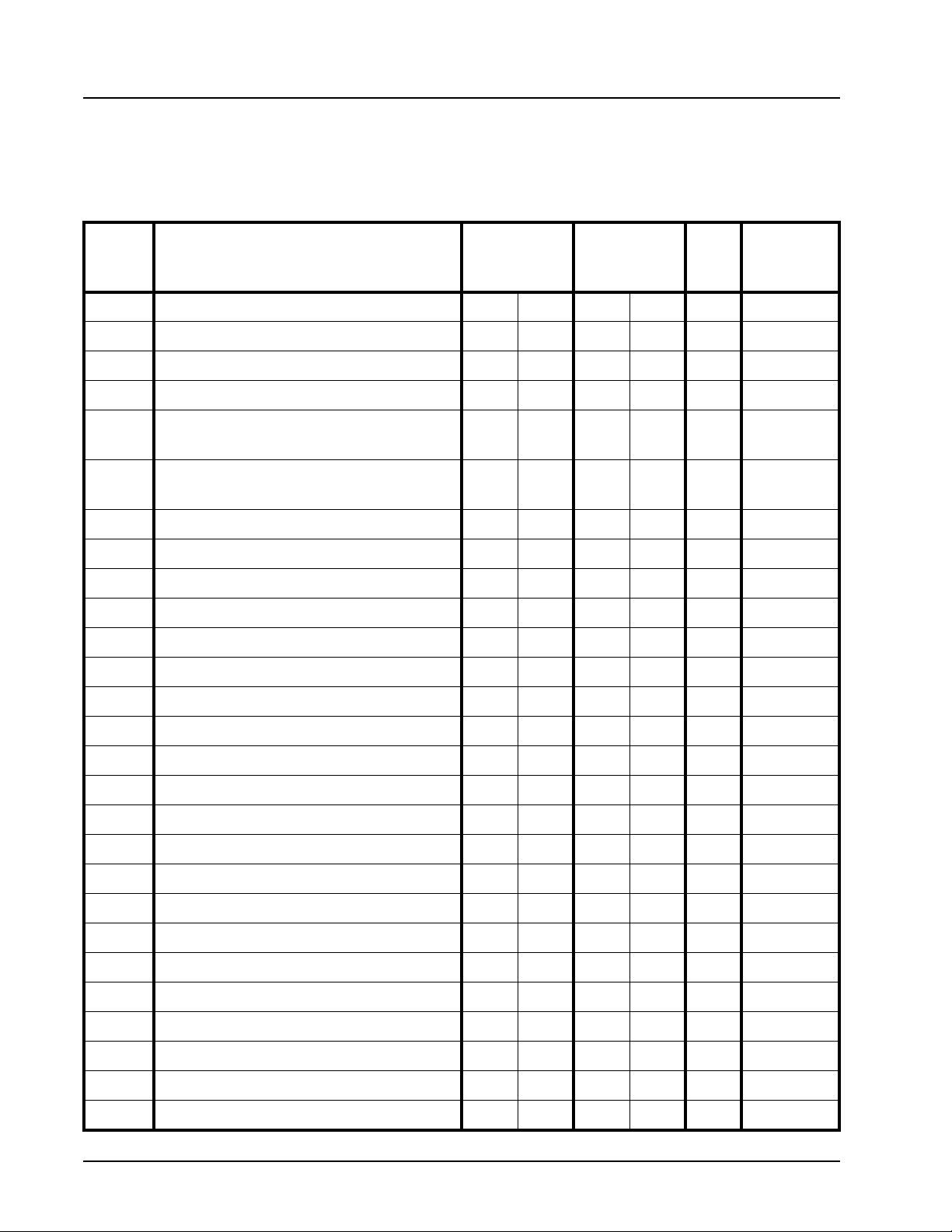
XR16C2850 xr
2.97V TO 5.5V DUAL UART WITH 128-BYTE FIFOS REV. 2.1.3
AC ELECTRICAL CHARACTERISTICS
O
TA=0
WHERE APPLICABLE
TO
70OC (-40O TO +85OC FOR INDUSTRIAL GRADE PACKAGE), VCC IS 2.90V TO 5.5V, 70 PF LOAD
LIMITS
SYMBOL PARAMETER
CLK Clock Pulse Duration 30 20 ns
OSC Oscillator Frequency 8 24 MHz
OSC External Clock Frequency 33 50 MHz
TAS Address Setup Time 5 0 ns
TAH Address Hold Time
(top mark date code of "DC YYWW" and older)
TAH Address Hold Time
(top mark date code of "F2 YYWW" and newer)
TCS Chip Select Width 66 50 ns
TRD IOR# Strobe Width 35 25 ns
TDY Read Cycle Delay 40 30 ns
TRDV Data Access Time 35 25 ns
TDD Data Disable Time 0 25 0 15 ns
TWR IOW# Strobe Width 40 25 ns
3.3
MIN MAX
10 5 ns
0 0 ns
LIMITS
5.0
MIN MAX
UNIT CONDITIONS
TDY Write Cycle Delay 40 30 ns
TDS Data Setup Time 20 15 ns
TDH Data Hold Time 5 5 ns
TWDO Delay From IOW# To Output 50 40 ns 100 pF load
TMOD Delay To Set Interrupt From MODEM Input 40 35 ns 100 pF load
TRSI Delay To Reset Interrupt From IOR# 40 35 ns 100 pF load
TSSI Delay From Stop To Set Interrupt 1 1 Bclk
TRRI Delay From IOR# To Reset Interrupt 45 40 ns 100 pF load
TSI Delay From Stop To Interrupt 45 40 ns
TINT Delay From Initial INT Reset To Transmit Start 8 24 8 24 Bclk
TWRI Delay From IOW# To Reset Interrupt 45 40 ns
TSSR Delay From Stop To Set RXRDY# 1 1 Bclk
TRR Delay From IOR# To Reset RXRDY# 45 40 ns
TWT Delay From IOW# To Set TXRDY# 45 40 ns
TSRT Delay From Center of Start To Reset TXRDY# 8 8 Bclk
40
Page 41
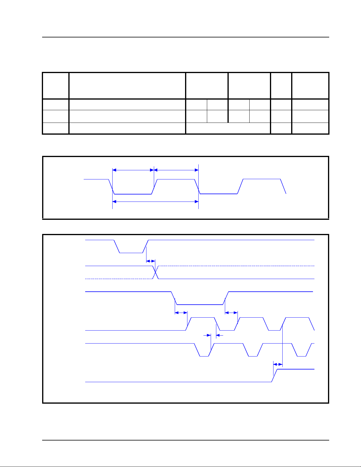
xr XR16C2850
REV. 2.1.3 2.97V TO 5.5V DUAL UART WITH 128-BYTE FIFOS
AC ELECTRICAL CHARACTERISTICS
O
TA=0
WHERE APPLICABLE
TO
70OC (-40O TO +85OC FOR INDUSTRIAL GRADE PACKAGE), VCC IS 2.90V TO 5.5V, 70 PF LOAD
SYMBOL PARAMETER
LIMITS
3.3
M
IN MAX
LIMITS
5.0
M
IN MAX
TRST Reset Pulse Width 40 40 ns
N Baud Rate Divisor 1
216-1
1
216-1
Bclk Baud Clock 16X or 8X of data rate Hz
FIGURE 16. CLOCK TIMING
CLK
EXTERNAL
CLOCK
OSC
CLK
FIGURE 17. MODEM INPUT/OUTPUT TIMING FOR CHANNELS A & B
IOW #
Active
UNIT CONDITIONS
-
RTS#
DTR#
CD#
CTS#
DSR#
INT
IOR#
RI#
Change of state
T
WDO
Change of state
T
MOD
Change of state
Active Active
Active
T
RSI
Change of state
T
MOD
Active
Active Active
T
MOD
Change of state
41
Page 42
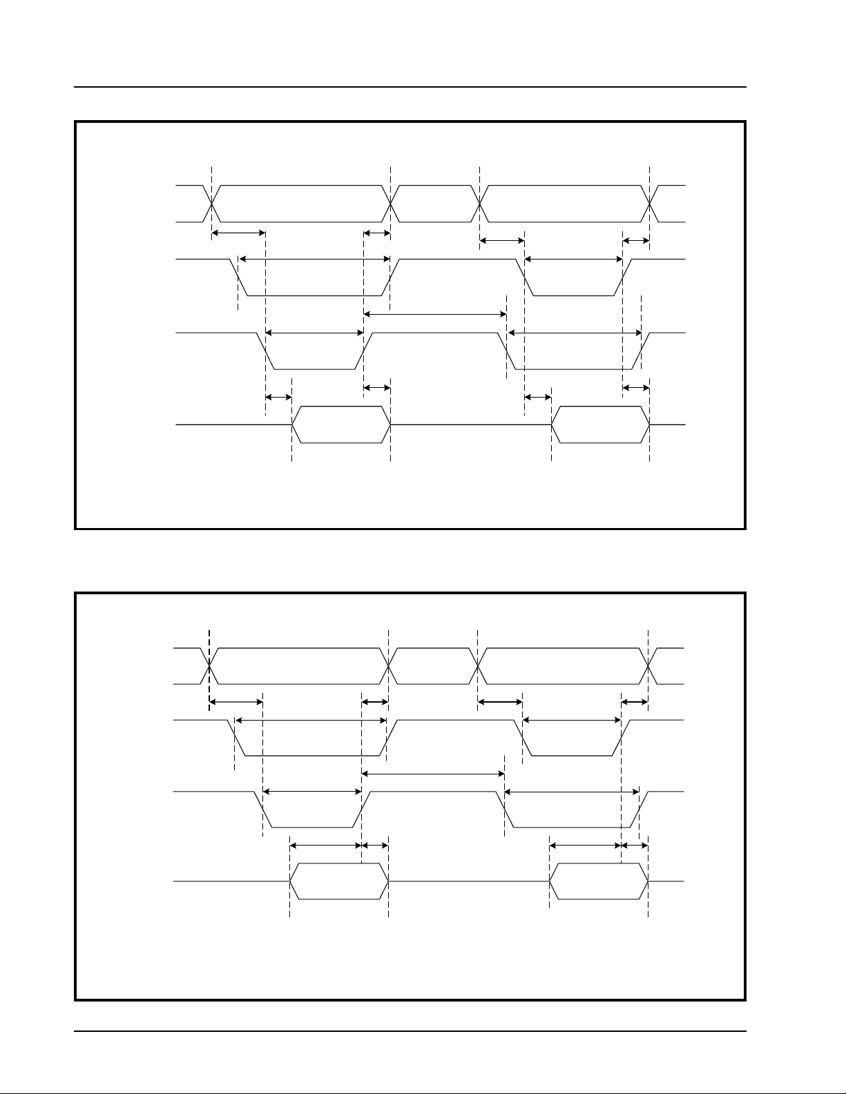
XR16C2850 xr
2.97V TO 5.5V DUAL UART WITH 128-BYTE FIFOS REV. 2.1.3
FIGURE 18. DATA BUS READ TIMING
A0-A2
T
AS
Valid Address Valid Address
CSA#/
CSB#
IOR#
T
RDV
D0-D7
FIGURE 19. DATA BUS WRITE TIMING
T
T
T
CS
T
RD
AH
T
DY
T
DD
AS
T
CS
T
RD
T
RDV
Valid Data Valid Data
T
AH
T
DD
RDTm
A0-A2
CSA#/
CSB#
IOW#
D0-D7
Valid Address Valid Address
T
AS
T
CS
T
WR
T
DS
T
AH
T
DY
T
DH
T
AS
T
CS
T
WR
T
DS
T
AH
T
DH
Valid Data Valid Data
16Write
42
Page 43
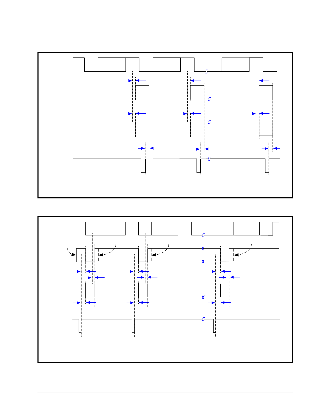
xr XR16C2850
REV. 2.1.3 2.97V TO 5.5V DUAL UART WITH 128-BYTE FIFOS
FIGURE 20. RECEIVE READY & INTERRUPT TIMING [NON-FIFO MODE] FOR CHANNELS A & B
RX
INT
RXRDY#
Start
Bit
D0:D7
Stop
Bit
T
T
SSR
1 Byte
in RHR
T
SSR
Active
Data
Ready
RR
D0:D7
in RHR
T
RR
T
SSR
1 Byte
T
SSR
Active
Data
Ready
D0:D7
IOR#
(Reading data
out of RHR)
FIGURE 21. TRANSMIT READY & INTERRUPT TIMING [NON-FIFO MODE] FOR CHANNELS A & B
1 Byte
in RHR
T
T
RR
T
SSR
SSR
Active
Data
Ready
RXNFM
TX
(Unloading)
IER[1]
enabled
Start
Bit
D0:D7
ISR is read ISR is readISR is read
Stop
Bit
D0:D7
INT*
T
WRI
T
WRI
T
SRT
T
SRT
TXRDY#
T
WT
T
WT
IOW#
(Loading data
into THR)
*INT is cleared when the ISR is read or when data is loaded into the THR.
D0:D7
T
WRI
T
SRT
T
WT
TXNonFIFO
43
Page 44
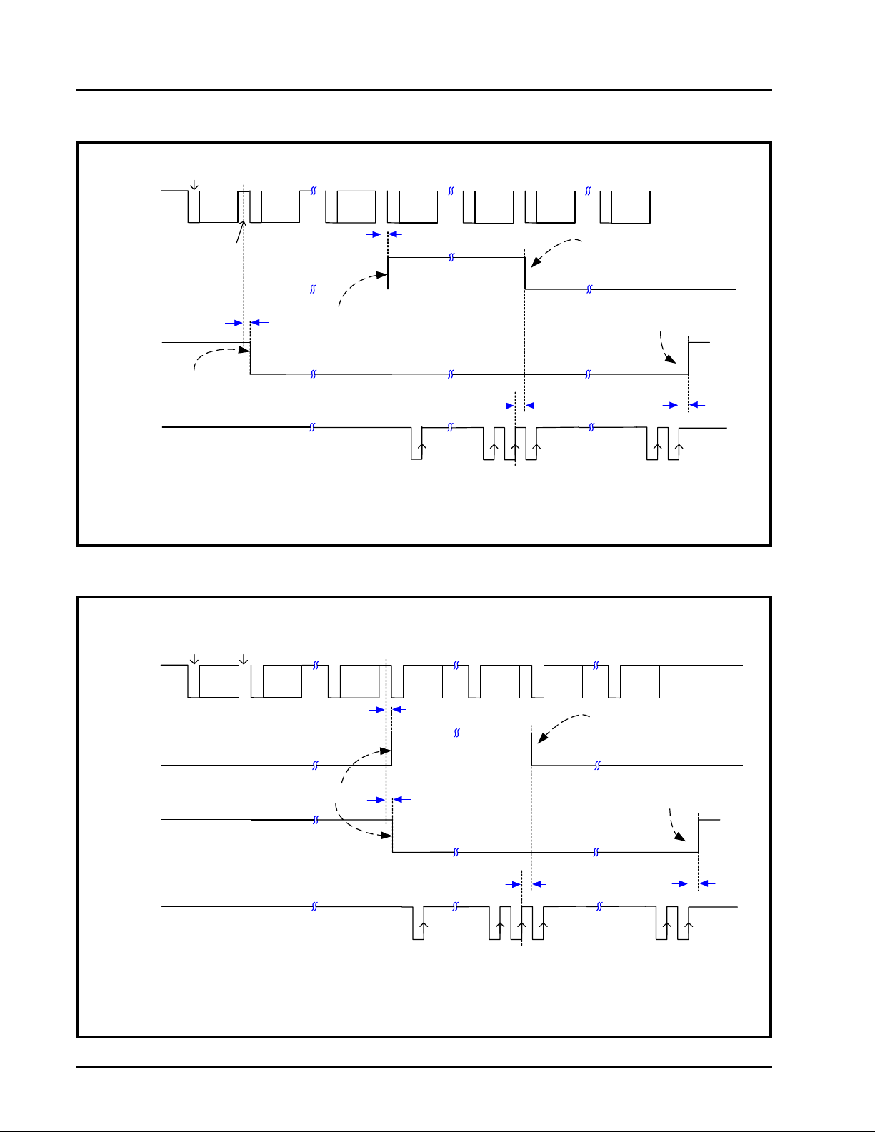
XR16C2850 xr
2.97V TO 5.5V DUAL UART WITH 128-BYTE FIFOS REV. 2.1.3
FIGURE 22. RECEIVE READY & INTERRUPT TIMING [FIFO MODE, DMA DISABLED] FOR CHANNELS A & B
Start
Bit
RX
S
D0:D7
Stop
Bit
S
D0:D7
D0:D7T D0:D7
S
T
SSI
S
D0:D7
T D0:D7
S
T
T
S
D0:D7
RX FIFO drops
below RX
T
Trigger Level
INT
T
SSR
RX FIFO fills up to RX
FIFO
Empties
Trigger Level or RX Data
RXRDY#
Timeout
First Byte is
Received in
RX FIFO
IOR#
(Reading data out
of RX FIFO)
T
RRI
T
RR
RXINTDMA#
FIGURE 23. RECEIVE READY & INTERRUPT TIMING [FIFO MODE, DMA ENABLED] FOR CHANNELS A & B
RX
INT
RXRDY#
IOR#
(Reading data out
of RX FIFO)
Start
Bit
S
Stop
Bit
D0:D7
RX FIFO fills up to RX
Trigger Level or RX Data
S
D0:D7
Timeout
D0:D7T D0:D7
S
T
SSI
T
SSR
S
D0:D7
T D0:D7
S
T
T
RRI
T
S
D0:D7
RX FIFO drops
below RX
Trigger Level
T
FIFO
Empties
T
RR
RXFIFODMA
44
Page 45
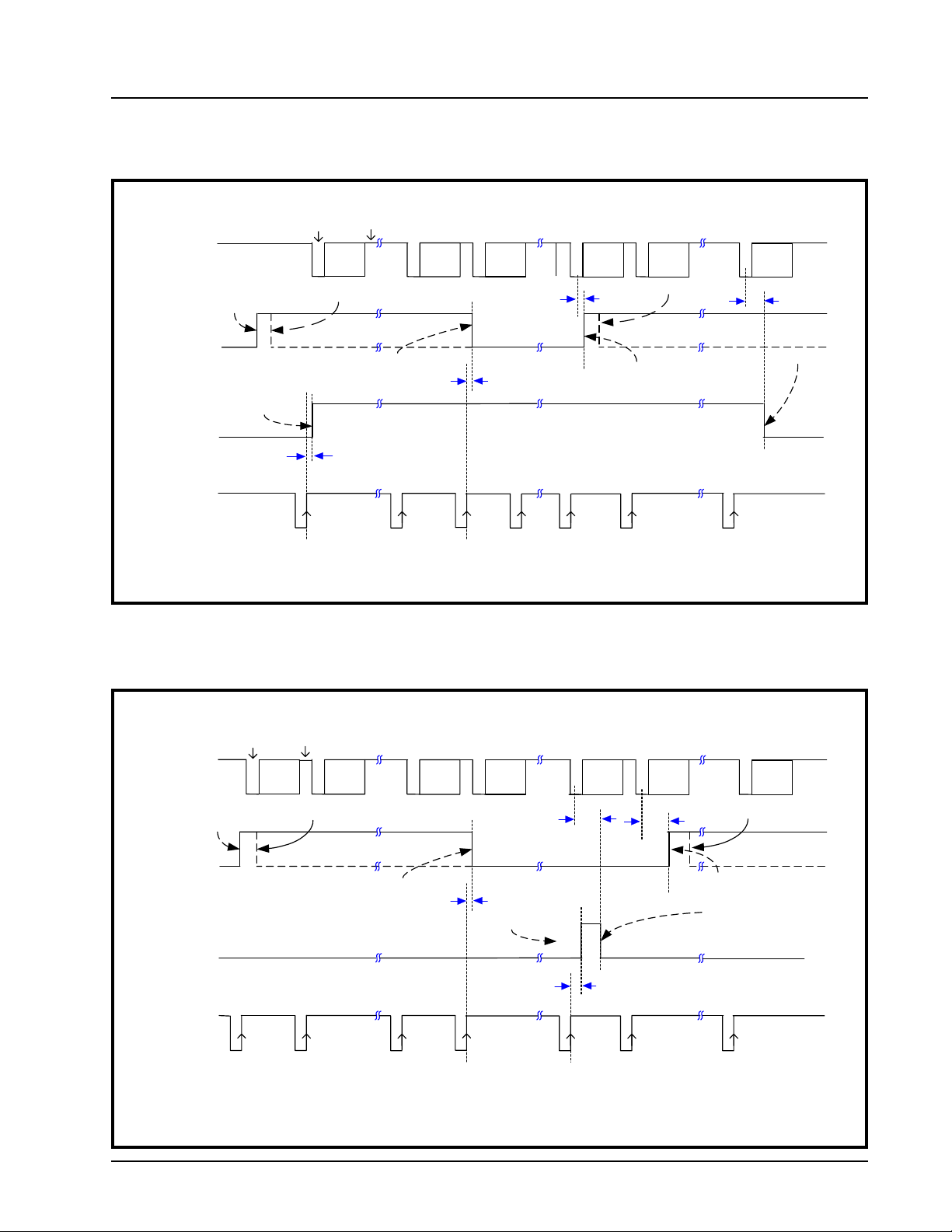
xr XR16C2850
REV. 2.1.3 2.97V TO 5.5V DUAL UART WITH 128-BYTE FIFOS
FIGURE 24. TRANSMIT READY & INTERRUPT TIMING [FIFO MODE, DMA MODE DISABLED] FOR CHANNELS A & B
TX
(Unloading)
TX FIFO
Empty
IER[1]
enabled
Start
Bit
S
D0:D7
ISR is read
Stop
Bit
D0:D7T D0:D7
S
TS
INT*
TX FIFO fills up
TXRDY#
Data in
TX FIFO
to trigger level
T
WT
T
IOW#
(Loading data
into FIFO)
*INT is cleared when the ISR is read or when TX FIFO fills up to the trigger level.
T
S
T D0:D7
WRI
D0:D7
T
SI
TX FIFO drops
below trigger level
S
T
ISR is read
Last Data Byte
Transmitted
T
S
D0:D7
TX FIFO
TXDMA#
T
SRT
Empty
T
FIGURE 25. TRANSMIT READY & INTERRUPT TIMING [FIFO MODE, DMA MODE ENABLED] FOR CHANNELS A & B
Start
Bit
TX
(Unloading)
IER[1]
enabled
INT*
TXRDY#
IOW#
(Loading data
into FIFO)
*INT cleared when the ISR is read or when TX FIFO fills up to trigger level.
Stop
Bit
S
D0:D7
S
T
ISR Read
D0:D7
TX FIFO fills up
to trigger level
T
D0:D7
S
D0:D7
T
WRI
TX FIFO
Full
T
T
D0:D7S
SRT
S
D0:D7
T
T
WT
T
T
SI
TX FIFO drops
below trigger level
Last Data Byte
ISR Read
At least 1
empty location
in FIFO
Transmitted
D0:D7S
TXDMA
T
45
Page 46
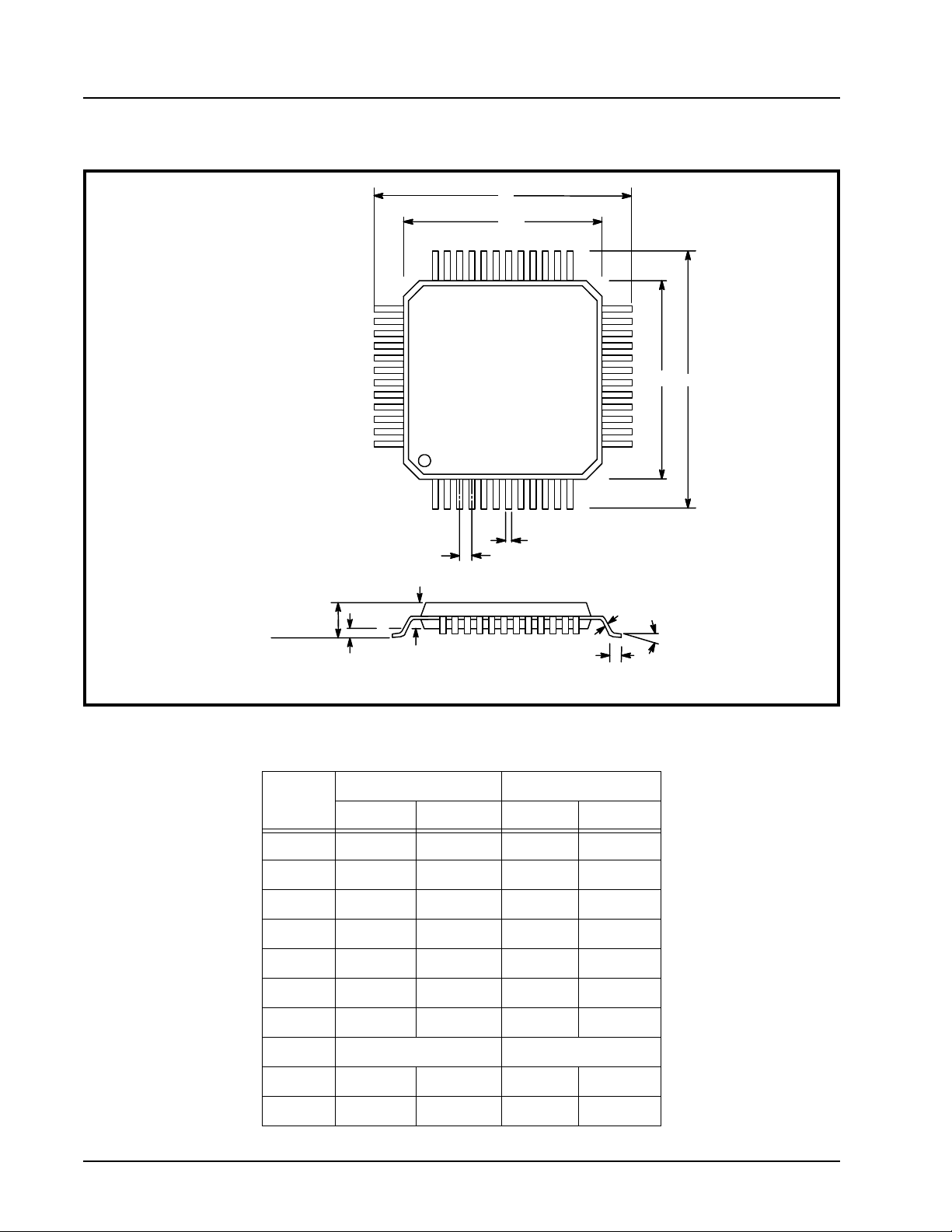
XR16C2850 xr
2.97V TO 5.5V DUAL UART WITH 128-BYTE FIFOS REV. 2.1.3
PACKAGE DIMENSIONS (48 PIN TQFP - 7 X 7 X 1 mm)
D
D
1
36 25
37
48
1
B
e
A
2
Seating
Plane
A
A
1
Note: The control dimension is the millimeter column
24
D
D
1
13
1
2
C
α
L
INCHES MILLIMETERS
SYMBOL MIN MAX MIN MAX
A 0.039 0.047 1.00 1.20
A1 0.002 0.006 0.05 0.15
A2 0.037 0.041 0.95 1.05
B 0.007 0.011 0.17 0.27
C 0.004 0.008 0.09 0.20
D 0.346 0.362 8.80 9.20
D1 0.272 0.280 6.90 7.10
e 0.020 BSC 0.50 BSC
L 0.018 0.030 0.45 0.75
a 0× 7× 0× 7×
46
Page 47
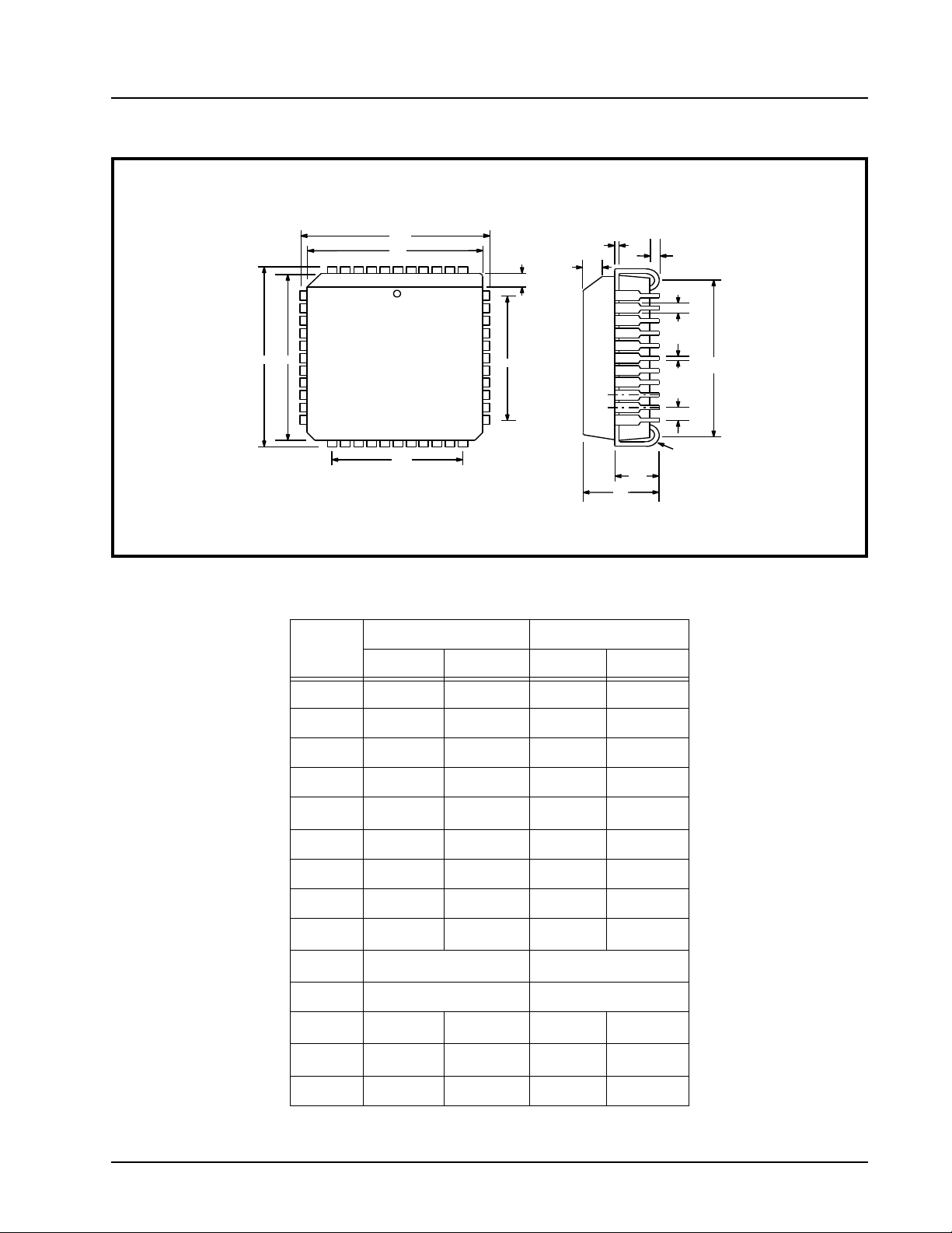
xr XR16C2850
REV. 2.1.3 2.97V TO 5.5V DUAL UART WITH 128-BYTE FIFOS
PACKAGE DIMENSIONS (44 PIN PLCC)
44 LEAD PLASTIC LEADED CHIP CARRIER
(PLCC)
Rev. 1.00
D
D
D D
1
1
244
1
D
3
°
x H
45
2
D
3
Note: The control dimension is the millimeter column
INCHES MILLIMETERS
45° x H
C
1
A
A
1
Seating Plane
A
2
B
1
B
D
e
R
2
SYMBOL MIN MAX MIN MAX
A 0.165 0.180 4.19 4.57
A1 0.090 0.120 2.29 3.05
A2 0.020 --- 0.51 ---
B 0.013 0.021 0.33 0.53
B
1
0.026 0.032 0.66 0.81
C 0.008 0.013 0.19 0.32
D 0.685 0.695 17.40 17.65
D1 0.650 0.656 16.51 16.66
D
2
D
3
0.590 0.630 14.99 16.00
0.500 typ. 12.70 typ.
e 0.050 BSC 1.27 BSC
H
1
H
2
0.042 0.056 1.07 1.42
0.042 0.048 1.07 1.22
R 0.025 0.045 0.64 1.14
47
Page 48
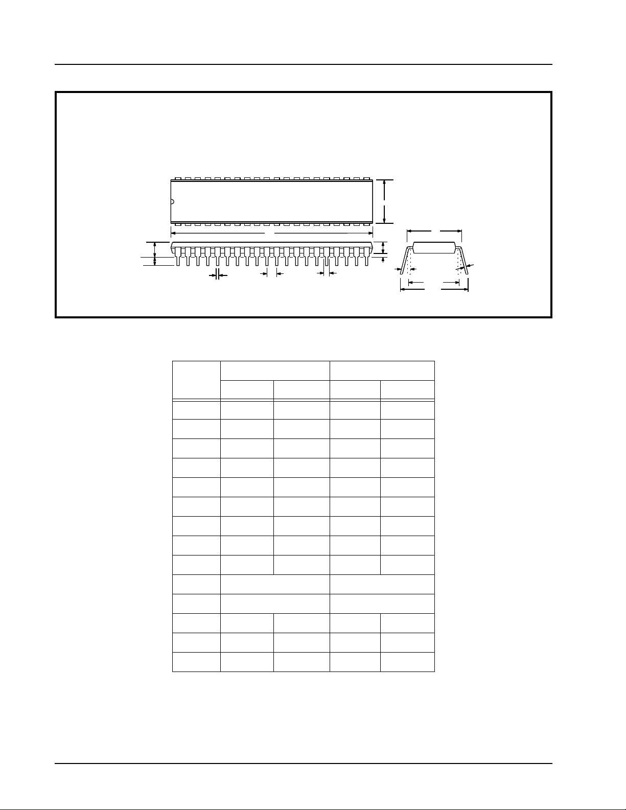
XR16C2850 xr
2.97V TO 5.5V DUAL UART WITH 128-BYTE FIFOS REV. 2.1.3
PACKAGE DIMENSIONS (40 PIN PDIP)
Seating
Plane
40
1
D
A
L
B
e
B
1
Note: The control dimension is the millimeter column
INCHES MILLIMETERS
SYMBOL MIN MAX MIN MAX
A 0.160 0.250 4.06 6.35
A1 0.015 0.070 0.38 1.78
A2 0.125 0.195 3.18 4.95
B 0.014 0.024 0.36 0.56
21
E
1
20
E
A
2
A
1
α
e
A
e
B
C
B1 0.030 0.070 0.76 1.78
C 0.008 0.014 0.20 0.38
D 1.98 2.095 50.29 53.21
E 0.600 0.625 15.24 15.88
E1 0.485 0.580 12.32 14.73
e 0.100 BSC 2.54 BSC
eA 0.600 BSC 15.24 BSC
eB 0.600 0.700 15.24 17.78
L 0.115 0.200 2.92 5.08
a 0× 15× 0× 15×
48
Page 49

xr XR16C2850
REV. 2.1.3 2.97V TO 5.5V DUAL UART WITH 128-BYTE FIFOS
REVISION HISTORY
Date Revision Description
February 2000 Rev 1.0.0 Initial datasheet.
April 2002 Rev 2.0.0 Changed to standard style format. Internal Registers are described in the order they
are listed in the Internal Register Table. Clarified timing diagrams. Corrected Auto
RTS Hysteresis table. Renamed Rclk (Receive Clock) to Bclk (Baud Clock) and tim
ing symbols. Added TAH, TCS and OSC.
May 2004 Rev 2.1.0 Changed to single column format. Added device status to ordering information.
Clarified sleep mode conditions. Clarified pin descriptions- changed from using logic
1 and logic 0 to HIGH (VCC) and LOW (GND) for input and output pin descriptions.
Added VOL sink current and VOH source current charts (
Figure 15). Devices with top mark date code of "F2 YYWW" and newer have 5V
tolerant inputs (except for XTAL1) and have 0 ns address hold time (TAH). DREV register was updated to 0x06.
February 2005 Rev 2.1.1 Corrected datasheet to show that all inputs are 5V tolerant (including XTAL1) in
devices with top mark date code of "F2 YYWW" and newer.
August 2005 Rev 2.1.2 Removed discontinued 40-pin PDIP from Ordering Information.
Figure 14 and
-
November 2005 Rev 2.1.3 Corrected part numbers in Ordering Information.
NOTICE
EXAR Corporation reserves the right to make changes to the products contained in this publication in order to
improve design, performance or reliability. EXAR Corporation assumes no responsibility for the use of any
circuits described herein, conveys no license under any patent or other right, and makes no representation that
the circuits are free of patent infringement. Charts and schedules contained here in are only for illustration
purposes and may vary depending upon a user’s specific application. While the information in this publication
has been carefully checked; no responsibility, however, is assumed for inaccuracies.
EXAR Corporation does not recommend the use of any of its products in life support applications where the
failure or malfunction of the product can reasonably be expected to cause failure of the life support system or
to significantly affect its safety or effectiveness. Products are not authorized for use in such applications unless
EXAR Corporation receives, in writing, assurances to its satisfaction that: (a) the risk of injury or damage has
been minimized; (b) the user assumes all such risks; (c) potential liability of EXAR Corporation is adequately
protected under the circumstances.
Copyright 2005 EXAR Corporation
Datasheet November 2005.
Send your UART technical inquiry with technical details to hotline: [email protected].
Reproduction, in part or whole, without the prior written consent of EXAR Corporation is prohibited.
49
Page 50

XR16C2850 xr
2.97V TO 5.5V DUAL UART WITH 128-BYTE FIFOS REV. 2.1.3
TABLE OF CONTENTS
GENERAL DESCRIPTION .................................................................................................1
APPLICATIONS................................................................................................................................................1
FEATURES .....................................................................................................................................................1
FIGURE 1. XR16C2850 BLOCK DIAGRAM ......................................................................................................................................... 1
FIGURE 2. PIN OUT ASSIGNMENT ..................................................................................................................................................... 2
ORDERING INFORMATION.................................................................................................................................2
PIN DESCRIPTIONS .........................................................................................................3
1.0 PRODUCT DESCRIPTION .....................................................................................................................7
2.0 FUNCTIONAL DESCRIPTIONS .............................................................................................................8
2.1 CPU INTERFACE .............................................................................................................................................. 8
FIGURE 3. XR16C2850 DATA BUS INTERCONNECTIONS ................................................................................................................. 8
2.2 DEVICE RESET ................................................................................................................................................ 8
2.3 DEVICE IDENTIFICATION AND REVISION ..................................................................................................... 8
2.4 CHANNEL A AND B SELECTION .................................................................................................................... 8
TABLE 1: CHANNEL A AND B SELECT ............................................................................................................................................... 9
2.5 CHANNEL A AND B INTERNAL REGISTERS ................................................................................................ 9
2.6 DMA MODE ....................................................................................................................................................... 9
TABLE 2: TABLE 2TXRDY# AND RXRDY# OUTPUTS IN FIFO AND DMA MODE ................................................................................ 9
2.7 INTA AND INTB OUPUTS .............................................................................................................................. 10
TABLE 3: INTA AND INTB PINS OPERATION FOR TRANSMITTER ...................................................................................................... 10
TABLE 4: INTA AND INTB PIN OPERATION FOR RECEIVER ............................................................................................................. 10
2.8 CRYSTAL OSCILLATOR OR EXTERNAL CLOCK INPUT ........................................................................... 10
FIGURE 4. TYPICAL OSCILLATOR CONNECTIONS............................................................................................................................... 10
2.9 PROGRAMMABLE BAUD RATE GENERATOR ........................................................................................... 11
FIGURE 5. EXTERNAL CLOCK CONNECTION FOR EXTENDED DATA RATE .......................................................................................... 11
FIGURE 6. BAUD RATE GENERATOR AND PRESCALER ..................................................................................................................... 11
TABLE 5: TYPICAL DATA RATES WITH A 14.7456 MHZ CRYSTAL OR EXTERNAL CLOCK ...................................................................... 12
2.10 TRANSMITTER ............................................................................................................................................. 12
2.10.1 TRANSMIT HOLDING REGISTER (THR) - WRITE ONLY ....................................................................................... 12
2.10.2 TRANSMITTER OPERATION IN NON-FIFO MODE ................................................................................................ 12
FIGURE 7. TRANSMITTER OPERATION IN NON-FIFO MODE .............................................................................................................. 13
2.10.3 TRANSMITTER OPERATION IN FIFO MODE ......................................................................................................... 13
FIGURE 8. TRANSMITTER OPERATION IN FIFO AND FLOW CONTROL MODE ..................................................................................... 13
2.11 RECEIVER .................................................................................................................................................... 14
2.11.1 RECEIVE HOLDING REGISTER (RHR) - READ-ONLY .......................................................................................... 14
FIGURE 9. RECEIVER OPERATION IN NON-FIFO MODE.................................................................................................................... 14
FIGURE 10. RECEIVER OPERATION IN FIFO AND AUTO RTS FLOW CONTROL MODE ....................................................................... 15
2.12 AUTO RTS (HARDWARE) FLOW CONTROL ............................................................................................. 15
2.13 AUTO RTS HYSTERESIS ............................................................................................................................ 15
2.14 AUTO CTS FLOW CONTROL ...................................................................................................................... 16
FIGURE 11. AUTO RTS AND CTS FLOW CONTROL OPERATION ....................................................................................................... 16
2.15 AUTO XON/XOFF (SOFTWARE) FLOW CONTROL ................................................................................... 17
TABLE 6: AUTO XON/XOFF (SOFTWARE) FLOW CONTROL ............................................................................................................... 17
2.16 SPECIAL CHARACTER DETECT ............................................................................................................... 17
2.17 AUTO RS485 HALF-DUPLEX CONTROL .................................................................................................. 17
2.18 INFRARED MODE ........................................................................................................................................ 18
FIGURE 12. INFRARED TRANSMIT DATA ENCODING AND RECEIVE DATA DECODING.......................................................................... 18
2.19 SLEEP MODE WITH AUTO WAKE-UP ....................................................................................................... 19
2.20 INTERNAL LOOPBACK .............................................................................................................................. 20
FIGURE 13. INTERNAL LOOP BACK IN CHANNELS A AND B .............................................................................................................. 20
3.0 UART INTERNAL REGISTERS ...........................................................................................................21
TABLE 7: UART CHANNEL A AND B UART INTERNAL REGISTERS...................................................................................... 21
TABLE 8: INTERNAL REGISTERS DESCRIPTION. SHADED BITS ARE ENABLED WHEN EFR BIT-4=1......................................... 22
4.0 INTERNAL REGISTER DESCRIPTIONS .............................................................................................23
4.1 RECEIVE HOLDING REGISTER (RHR) - READ- ONLY ............................................................................... 23
4.2 TRANSMIT HOLDING REGISTER (THR) - WRITE-ONLY ............................................................................ 23
4.3 INTERRUPT ENABLE REGISTER (IER) - READ/WRITE .............................................................................. 23
4.3.1 IER VERSUS RECEIVE FIFO INTERRUPT MODE OPERATION ............................................................................. 23
4.3.2 IER VERSUS RECEIVE/TRANSMIT FIFO POLLED MODE OPERATION ................................................................ 24
I
Page 51

xr XR16C2850
REV. 2.1.3 2.97V TO 5.5V DUAL UART WITH 128-BYTE FIFOS
4.4 INTERRUPT STATUS REGISTER (ISR) - READ-ONLY ............................................................................... 25
4.4.1 INTERRUPT GENERATION: ...................................................................................................................................... 25
4.4.2 INTERRUPT CLEARING: ........................................................................................................................................... 25
TABLE 9: INTERRUPT SOURCE AND PRIORITY LEVEL ....................................................................................................................... 25
4.5 FIFO CONTROL REGISTER (FCR) - WRITE-ONLY ..................................................................................... 26
TABLE 10: TRANSMIT AND RECEIVE FIFO TRIGGER TABLE AND LEVEL SELECTION .......................................................................... 27
4.6 LINE CONTROL REGISTER (LCR) - READ/WRITE ..................................................................................... 28
TABLE 11: PARITY SELECTION ........................................................................................................................................................ 29
4.7 MODEM CONTROL REGISTER (MCR) OR GENERAL PURPOSE OUTPUTS CONTROL - READ/WRITE 29
4.8 LINE STATUS REGISTER (LSR) - READ ONLY ........................................................................................... 30
4.9 MODEM STATUS REGISTER (MSR) - READ ONLY .................................................................................... 31
4.10 SCRATCH PAD REGISTER (SPR) - READ/WRITE .................................................................................... 32
4.11 ENHANCED MODE SELECT REGISTER (EMSR) ...................................................................................... 32
TABLE 12: SCRATCHPAD SWAP SELECTION .................................................................................................................................... 32
TABLE 13: EXTENDED RTS HYSTERESIS ........................................................................................................................................ 33
4.12 FIFO LEVEL REGISTER (FLVL) - READ-ONLY ......................................................................................... 33
4.13 BAUD RATE GENERATOR REGISTERS (DLL AND DLM) - READ/WRITE .............................................. 33
4.14 DEVICE IDENTIFICATION REGISTER (DVID) - READ ONLY .................................................................... 33
4.15 DEVICE REVISION REGISTER (DREV) - READ ONLY .............................................................................. 33
4.16 TRIGGER LEVEL / FIFO DATA COUNT REGISTER (TRG) - WRITE-ONLY ............................................. 34
4.17 FIFO DATA COUNT REGISTER (FC) - READ-ONLY ................................................................................. 34
4.18 FEATURE CONTROL REGISTER (FCTR) - READ/WRITE ....................................................................... 34
TABLE 14: TRIGGER TABLE SELECT ............................................................................................................................................... 34
4.19 ENHANCED FEATURE REGISTER (EFR) .................................................................................................. 35
TABLE 15: SOFTWARE FLOW CONTROL FUNCTIONS ........................................................................................................................ 35
4.20 SOFTWARE FLOW CONTROL REGISTERS (XOFF1, XOFF2, XON1, XON2) - READ/WRITE ................ 36
TABLE 16: UART RESET CONDITIONS FOR CHANNEL A AND B............................................................................................ 37
ABSOLUTE MAXIMUM RATINGS .................................................................................. 38
TYPICAL PACKAGE THERMAL RESISTANCE DATA (MARGIN OF ERROR: ± 15%) 38
ELECTRICAL CHARACTERISTICS................................................................................ 38
DC ELECTRICAL CHARACTERISTICS.............................................................................................................. 38
FIGURE 14. XR16C2850 VOL SINK CURRENT CHART ................................................................................................................... 39
FIGURE 15. XR16C2850 VOH SOURCE CURRENT CHART ............................................................................................................. 39
AC ELECTRICAL CHARACTERISTICS.............................................................................................................. 40
TA=0O TO 70OC (-40O TO +85OC FOR INDUSTRIAL GRADE PACKAGE), VCC IS 2.90V TO 5.5V, 70 PF LOAD WHERE
APPLICABLE ................................................................................................................................................. 40
FIGURE 16. CLOCK TIMING............................................................................................................................................................. 41
FIGURE 17. MODEM INPUT/OUTPUT TIMING FOR CHANNELS A & B ................................................................................................. 41
FIGURE 19. DATA BUS WRITE TIMING ............................................................................................................................................ 42
FIGURE 18. DATA BUS READ TIMING .............................................................................................................................................. 42
FIGURE 20. RECEIVE READY & INTERRUPT TIMING [NON-FIFO MODE] FOR CHANNELS A & B ......................................................... 43
FIGURE 21. TRANSMIT READY & INTERRUPT TIMING [NON-FIFO MODE] FOR CHANNELS A & B ....................................................... 43
FIGURE 22. RECEIVE READY & INTERRUPT TIMING [FIFO MODE, DMA DISABLED] FOR CHANNELS A & B........................................ 44
FIGURE 23. RECEIVE READY & INTERRUPT TIMING [FIFO MODE, DMA ENABLED] FOR CHANNELS A & B......................................... 44
FIGURE 24. TRANSMIT READY & INTERRUPT TIMING [FIFO MODE, DMA MODE DISABLED] FOR CHANNELS A & B ........................... 45
FIGURE 25. TRANSMIT READY & INTERRUPT TIMING [FIFO MODE, DMA MODE ENABLED] FOR CHANNELS A & B ............................ 45
PACKAGE DIMENSIONS (48 PIN TQFP - 7 X 7 X 1 mm)................................................ 46
PACKAGE DIMENSIONS (44 PIN PLCC) ....................................................................... 47
PACKAGE DIMENSIONS (40 PIN PDIP) ........................................................................ 48
REVISION HISTORY ...................................................................................................................................... 49
TABLE OF CONTENTS ............................................................................................................ I
II
 Loading...