

Datasheet MAX4375TEUB, MAX4375TESD, MAX4375HEUB, MAX4375FESD, MAX4374TEUB Datasheet (Maxim)
...
For free samples and the latest literature, visit www.maxim-ic.com or phone 1-800-998-8800.
For small orders, phone 1-800-835-8769.
General Description
The MAX4373/MAX4374/MAX4375 low-cost, micropower, high-side current-sense supervisors contain a highside current-sense amplifier, bandgap reference, and
comparator with latching output. They feature a voltage
output that eliminates the need for gain-setting resistors,
making them ideal for today’s notebook computers, cell
phones, and other systems where battery/DC current
monitoring is critical. High-side current monitoring is
especially useful in battery-powered systems since it
does not interfere with the ground path of the battery
charger. The 0 to +28V input common-mode range is
independent of the supply voltage, which ensures that
the current-sense feedback remains viable even when
connected to a battery pack in deep discharge.
The comparator output of the MAX4373/MAX4374/
MAX4375 is latched to provide a turn-off flag that
doesn’t oscillate. In addition, the MAX4374/MAX4375
contain a second comparator for use in window-detection functions. The MAX4373/MAX4374/MAX4375 are
available in three different gain versions (T = +20V/V,
F = +50V/V, H = +100V/V) and use an external sense
resistor to set the sensitivity of the input voltage to the
load current. These features offer a high level of integration, resulting in a simple and compact currentsense solution.
The MAX4373/MAX4374/MAX4375 operate from a single +2.7V to +28V supply and consume 50µA. They are
specified for the extended operating temperature range
(-40°C to +85°C) and are available in 8-pin and 10-pin
µMAX packages.
________________________Applications
Notebook Computers
Portable/Battery-Powered Systems
Smart Battery Packs/Chargers
Cell Phones
Power-Management Systems
General-System/Board-Level Current Monitoring
Precision Current Sources
Features
♦ Current-Sense Amplifier plus Internal Comparator
and Bandgap Reference
♦ 50µA Supply Current
♦ Single +2.7V to +28V Operating Supply
♦ 0.66% Full-Scale Accuracy
♦ Internal Bandgap Reference
♦ Latching Comparator Output
♦ Three Gain Versions Available (+20V/V, +50V/V,
+100V/V)
♦ Wide 0 to +28V Common-Mode Range,
Independent of Supply Voltage
MAX4373/MAX4374/MAX4375
Low-Cost, Micropower, High-Side Current-Sense
Amplifier + Comparator + Reference ICs
________________________________________________________________ Maxim Integrated Products 1
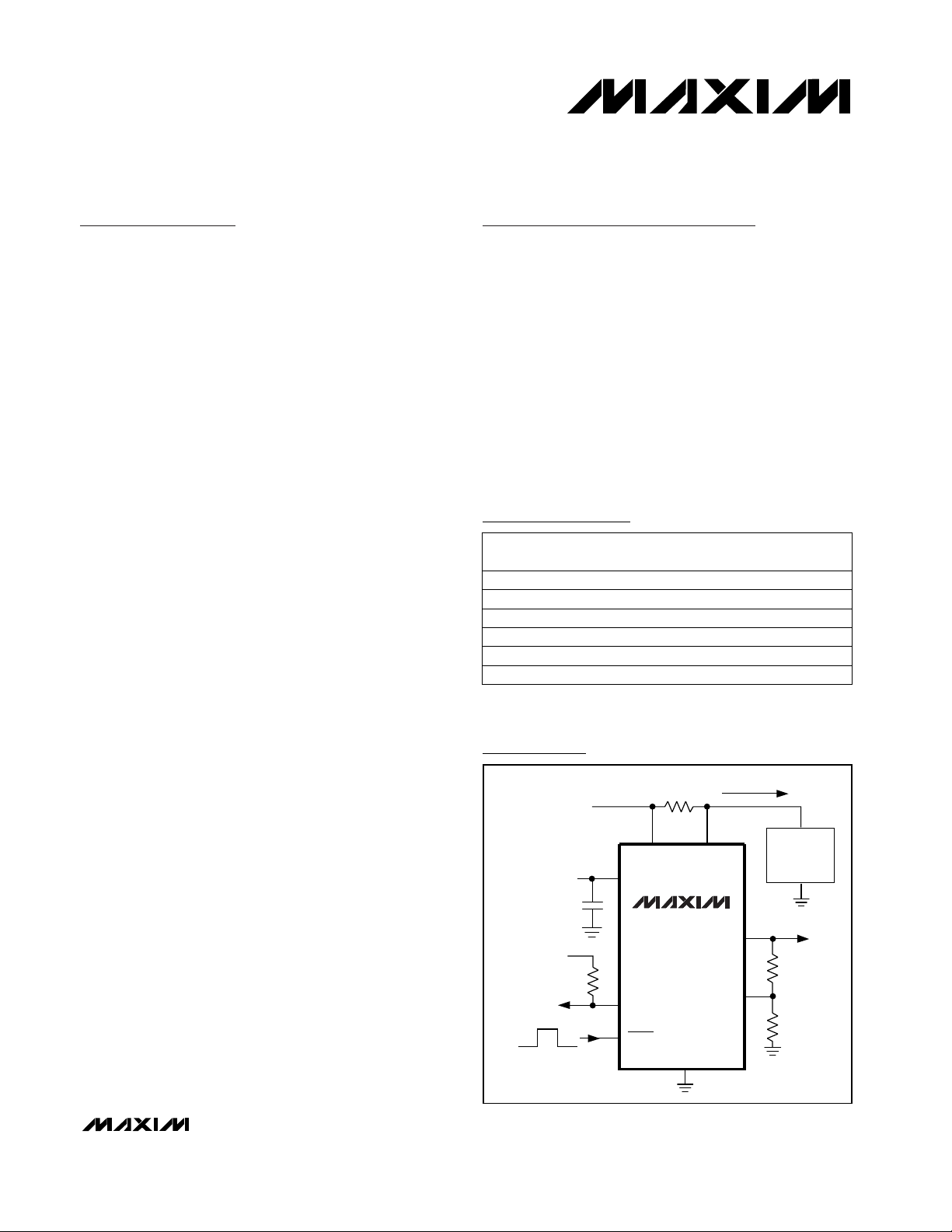
Typical Operating Circuit
19-1630; Rev 0; 3/00
Pin Configurations appear at end of data sheet.
8 SO
8 µMAX
PIN-
PACKAGE
TEMP. RANGE
-40°C to +85°C
-40°C to +85°CMAX4373TESA
MAX4373TEUA
PART
+20
+20
GAIN
(V/V)
8 µMAX-40°C to +85°CMAX4373FEUA +50
8 SO-40°C to +85°CMAX4373FESA +50
8 µMAX-40°C to +85°CMAX4373HEUA +100
8 SO-40°C to +85°CMAX4373HESA +100
Ordering Information continues at end of data sheet.
Ordering Information
+ V
V
CC
COUT
RESET
SENSE
R
SENSE
MAX4373
GND
VIN = 0 TO 28V
VCC = 2.7V TO 28V
0.1µF
V
= 5V
PULL-UP
C1
R3
I
LOAD
-
RS-RS+
OUT
CIN
LOAD/
BATTERY
R1
R2
MAX4373/MAX4374/MAX4375
Low-Cost, Micropower, High-Side Current-Sense
Amplifier + Comparator + Reference ICs
2 _______________________________________________________________________________________
ABSOLUTE MAXIMUM RATINGS
ELECTRICAL CHARACTERISTICS
(VCC= +2.7V to +28V, V
RS+
= 0 to +28V, V
SENSE
= 0, V
RESET
= 0, R
LOAD
= 1MΩ, TA= T
MIN
to T
MAX
, unless otherwise noted. Typical
values are at T
A
= +25°C.) (Note 1)
Stresses beyond those listed under “Absolute Maximum Ratings” may cause permanent damage to the device. These are stress ratings only, and functional
operation of the device at these or any other conditions beyond those indicated in the operational sections of the specifications is not implied. Exposure to
absolute maximum rating conditions for extended periods may affect device reliability.
VCC, RS+, RS- to GND ...........................................-0.3V to +30V
OUT to GND ................................................-0.3V to the lesser of
(V
CC
+ 0.3V) or +15V
CIN1, CIN2, RESET to GND ........................-0.3V to the lesser of
(V
CC
+ 0.3V) or +12V
Differential Input Voltage (V
RS
+ - VRS-)..............................±0.3V
COUT1, COUT2 to GND........................................-0.3V to +6.0V
Current into Any Pin..........................................................±10mA
Continuous Power Dissipation (T
A
= +70°C)
8-Pin µMAX (derate 4.1mW/°C above +70°C) .............330mW
8-Pin SO (derate 5.9mW/°C above +70°C)..................471mW
10-Pin µMAX (derate 5.6mW/°C above +70°C) ...........444mW
14-Pin SO (derate 8.3mW/°C above +70°C)................667mW
Operating Temperature Range ...........................-40°C to +85°C
Junction Temperature......................................................+150°C
Storage Temperature Range .............................-65°C to +150°C
Lead Temperature (soldering, 10s) .................................+300°C
%
Total OUT Voltage Error
(Note 5)
V
SENSE
= 100mV
(Note 6)
V
SENSE
= 6.25mV, VCC= 12V, V
RS+
= 12V
(Note 7)
VCC= 12V,
V
RS+
= 0.1V
VCC= 28V, V
RS+
= 28V,
TA= T
MIN
to T
MAX
VCC= 12V, V
RS+
= 12V,
TA= T
MIN
to T
MAX
%
8.5 65I
OUT
= 100µA
I
OUT
= 10µA
±7.5
±0.55 ±7.5
±5.0
±5.0
PARAMETER SYMBOL MIN TYP MAX UNITS
-25 2.0
Input Bias Current
I
RS+
0 2.5
µA
Leakage Current I
RS+, IRS-
±0.015 ±0.5 µA
Supply Current I
CC
50 100 µA
I
RS-
04
-50 4
Full-Scale Sense Voltage
(Note 4)
V
SENSE
150 170
mV
100 120
Common-Mode Input Range
(Note 3)
Operating Voltage Range
(Note 2)
V
CC
2.7 28 V
V
CMR
028V
Common-Mode Rejection CMR 85 dB
OUT Voltage Low V
OUT
2.5
mV
OUT Voltage High
V
CC -
V
OH
0.25 V
CONDITIONS
V
RS+
≤ 2V
VCC= 2.7V
V
RS+
> 2V
V
CC
= 0
V
RS+
> 2V, V
SENSE
= 5mV
V
RS+
> 2V
V
RS+
≤ 2V
VCC= 2.7V, I
OUT
= -500µA
Gain = +20V/V, +50V/V
Gain = +100V/V
V
RS+
> 2V
Full-Scale Accuracy
(Note 5)
V
SENSE
= 100mV, VCC= 12V, V
RS+
= 12V,
TA= +25°C
±0.66 ±5.5
MAX4373/MAX4374/MAX4375
Low-Cost, Micropower, High-Side Current-Sense
Amplifier + Comparator + Reference ICs
_______________________________________________________________________________________ 3
V
SENSE
=
20mV to 150mV;
V
CC
= 12V; V
RS+
= 12V;
Gain = 20, 50
MAX437_T
V
RS+
= 12V,
VCC= 12V,
C
LOAD
= 10pF
V
SENSE
= 100mV, C
LOAD
= 10pF,
V
CC
= 12V, V
RS+
= 12V
Gain = +20V/V,
V
CC
= 12V,
V
RS+
= 12V,
C
LOAD
= 10pF
No sustained oscillations
V
SENSE
= 100mV
V
OUT
= 2V, V
RS+
> 2V
CONDITIONS
%
±0.64 ±5.2
∆A
V
Gain Accuracy
V/V
+20
A
V
kHz
200
BW-3dB Bandwidth
Gain
mV580 600 618Comparator Threshold
0.5
µs
20
OUT Settling Time to 1% of
Final Value
pF1000Capacitive Load Stability
Ω1.5R
OUT
OUT Output Resistance
72 87
UNITSMIN TYP MAXSYMBOLPARAMETER
120
110
50
V
SENSE
= 100mV,
Gain = +20V/V
V
SENSE
= 100mV,
Gain = +50V/V
V
SENSE
= 100mV,
Gain = +100V/V
V
SENSE
= 6.25mV
MAX437_H
MAX437_F
+100
+50
TA= +25°C
TA= -40°C to +85°C ±7.2
V
SENSE
= 6.25mV to
100mV
V
SENSE
= 100mV to
6.25mV
20
PSR
Power-Up Time to 1% of Final
Value
Power-Supply Rejection
ms
dB
VCC= 12V, V
RS+
= 12V, C
LOAD
= 10pF
Saturation Recovery Time
(Note 8)
ms0.1
mV-9Comparator Hysteresis
nA±2.2 ±15I
B
Input Bias Current
CL= 10pF, RL= 10kΩ pull-up to 5V,
5mV of overdrive
µs4Propagation Delay
I
SINK
= 1mA V0.6V
OL
Output Low Voltage
V
SENSE
=
20mV to 100mV,
V
CC
= 12V, V
RS+
= 12V,
Gain = 100
TA= +25°C
TA= -40°C to +85°C ±7.2
±0.62 ±5.0
COMPARATOR (Note 9)
ELECTRICAL CHARACTERISTICS (continued)
(VCC= +2.7V to +28V, V
RS+
= 0 to +28V, V
SENSE
= 0, V
RESET
= 0, R
LOAD
= 1MΩ, TA= T
MIN
to T
MAX
, unless otherwise noted. Typical
values are at T
A
= +25°C.) (Note 1)
0
20
10
40
30
50
60
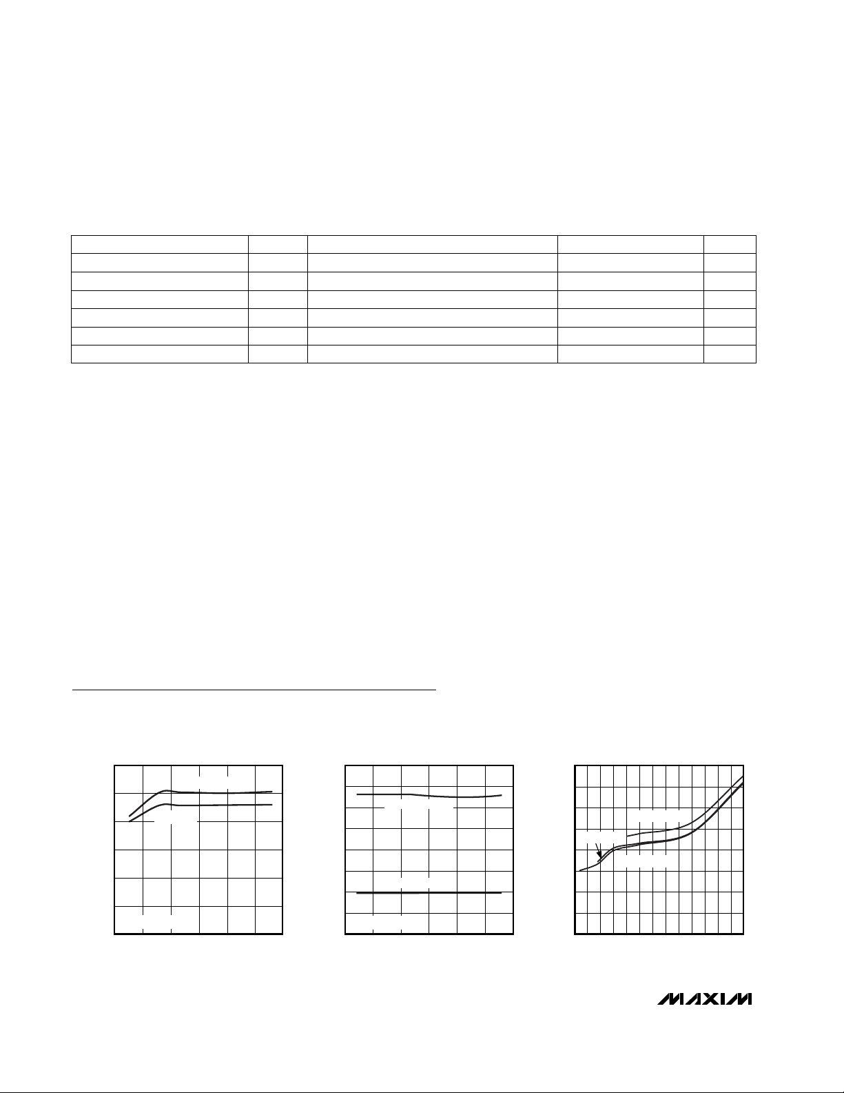
010155 202530
SUPPLY CURRENT
vs. SUPPLY VOLTAGE
MAX4373 toc01
SUPPLY VOLTAGE (V)
SUPPLY CURRENT (µA)
MAX4373
MAX4374/MAX4375
V
SENSE
= 5mV
44
45
46
47
48
49
50
51
52
0105 15202530
SUPPLY CURRENT
vs. COMMON-MODE VOLTAGE
MAX4373 toc02
COMMON-MODE VOLTAGE (V)
SUPPLY CURRENT (µA)
MAX4374/MAX4375
MAX4373
V
SENSE
= 5mV
-2.0
-0.5
-1.0
-1.5
0
0.5
1.5
1.0
2.0
2684 10121416182022242628
TOTAL OUTPUT ERROR
vs. SUPPLY VOLTAGE
MAX4373 toc03
SUPPLY VOLTAGE (V)
OUTPUT ERROR (%)
AV = +100V/V
AV = +20V/V
AV = +50V/V
Typical Operating Characteristics
(V
RS+
= +12V, V
CC
= +12V, R
LOAD
= 1MΩ, V
RESET
= 0, V
SENSE
= 100mV, V
PULL-UP
= +5V, R
PULL-UP
= 10kΩ, TA= +25°C, unless
otherwise noted.)
MAX4373/MAX4374/MAX4375
Low-Cost, Micropower, High-Side Current-Sense
Amplifier + Comparator + Reference ICs
4 _______________________________________________________________________________________
Note 1: All devices are 100% production tested at TA= +25°C. All temperature limits are guaranteed by design.
Note 2: Guaranteed by PSR test.
Note 3: Guaranteed by OUT Voltage Error test.
Note 4: Guaranteed by Gain Accuracy test. Output voltage is internally clamped not to exceed 12V.
Note 5: Total OUT Voltage Error and Full-Scale Accuracy are the sum of gain and offset voltage errors.
Note 6: Measured at I
OUT
= -500µA (R
LOAD
= 4kΩ for gain of +20V/V, R
LOAD
= 10kΩ for gain of +50V/V, R
LOAD
= 20kΩ for gain of
+100V/V).
Note 7: +6.25mV = 1/16 of +100mV full-scale voltage.
Note 8: The device will not experience phase reversal when overdriven.
Note 9: All comparator tests are done with V
RS+
= +12V.
Note 10: V
PULL-UP
is defined as an externally applied voltage through a resistor to pull up the comparator output.
ELECTRICAL CHARACTERISTICS (continued)
(VCC= +2.7V to +28V, V
RS+
= 0 to +28V, V
SENSE
= 0, V
RESET
= 0, R
LOAD
= 1MΩ, TA= T
MIN
to T
MAX
, unless otherwise noted. Typical
values are at T
A
= +25°C.) (Note 1)
VCC= 28V, V
PULL-UP
= 5V (Note 10)
CONDITIONS
µA1Output High Leakage Current
UNITSINTYP MAXSYMBOLPARAMETER
V2.0V
IH
RESET Input High Voltage
V0.8V
IL
RESET Input Low Voltage
V
IL
= 0, VIH= 5.5V, VCC= 28V µA-0.5 0.5IIL, I
IH
Logic Input Current
µs3t
RPD
RESET Propagation Delay
µs1.5t
RPW
Minimum RESET Pulse Width

MAX4373/MAX4374/MAX4375
Low-Cost, Micropower, High-Side Current-Sense
Amplifier + Comparator + Reference ICs
_______________________________________________________________________________________ 5
Typical Operating Characteristics (continued)
(V
RS+
= +12V, V
CC
= +12V, R
LOAD
= 1MΩ, V
RESET
= 0, V
SENSE
= 100mV, V
PULL-UP
= +5V, R
PULL-UP
= 10kΩ, TA= +25°C, unless
otherwise noted.)
INPUT
OUTPUT
20µs/div
1V
3V
30mV
10mV
SMALL-SIGNAL PULSE RESPONSE
(A
V
= +100V/V)
MAX4373 toc11
TOTAL OUTPUT ERROR
vs. SUPPLY VOLTAGE
5
4
3
AV = +100V/V
2
1
0
-1
OUTPUT ERROR (%)
-2
-3
-4
-5
2684 10121416182022242628
AV = +50V/V
AV = +20V/V
SUPPLY VOLTAGE (V)
3.0
2.5
2.0
1.5
OUTPUT ERROR (%)
1.0
0.5
0
0507525 100 125 150
MAX4373 toc04
TOTAL OUTPUT ERROR
vs. SENSE VOLTAGE
AV = +100V/V
AV = +20V/V
V
(mV)
SENSE
1.5
VCC = +5.5V
1.0
0.5
AV = +100V/V
0
-0.5
-1.0
OUTPUT ERROR (%)
-1.5
-2.0
-2.5
05025 75 100 125 150
VCC = +28V
AV = +50V/V
TOTAL OUTPUT ERROR
vs. SENSE VOLTAGE
AV = +20V/V
AV = +50V/V
V
(mV)
SENSE
MAX4373 toc07
TOTAL OUTPUT ERROR
2.0
1.5
MAX4373 toc05
1.0
0.5
0
-0.5
OUTPUT ERROR (%)
-1.0
-1.5
-2.0
AV = +100V/V
05025 75 100 125 150
TOTAL OUTPUT ERROR
vs. COMMON-MODE VOLTAGE
12
10
AV = +100V/V
8
6
4
OUTPUT ERROR (%)
AV = +50V/V
2
0
AV = +20V/V
-2
2684 10121416182022242628
COMMON-MODE VOLTAGE (V)
vs. SENSE VOLTAGE
AV = +20V/V
AV = +50V/V
V
(mV)
SENSE
MAX4373 toc08
MAX4373 toc06
SMALL-SIGNAL PULSE RESPONSE
= +20V/V)
(A
V
INPUT
OUTPUT
SMALL-SIGNAL PULSE RESPONSE
= +50V/V)
(A
MAX4373 toc09
30mV
10mV
20µs/div
600mV
200mV
INPUT
OUTPUT
V
20µs/div
MAX4373 toc10
30mV
10mV
1.5V
500mV

MAX4373/MAX4374/MAX4375
Low-Cost, Micropower, High-Side Current-Sense
Amplifier + Comparator + Reference ICs
6 _______________________________________________________________________________________
Typical Operating Characteristics (continued)
(V
RS+
= +12V, V
CC
= +12V, R
LOAD
= 1MΩ, V
RESET
= 0, V
SENSE
= 100mV, V
PULL-UP
= +5V, R
PULL-UP
= 10kΩ, TA= +25°C, unless
otherwise noted.)
INPUT
OUTPUT
20µs/div
1V
3V
150mV
50mV
LARGE-SIGNAL PULSE RESPONSE
(A
V
= +20V/V)
MAX4373 toc12
INPUT
OUTPUT
20µs/div
2.5V
7.5V
150mV
50mV
LARGE-SIGNAL PULSE RESPONSE
(A
V
= +50V/V)
MAX4373 toc13
INPUT
OUTPUT
20µs/div
500mV
9.5V
95mV
5mV
LARGE-SIGNAL PULSE RESPONSE
(A
V
= +100V/V)
MAX4373 toc14
0
-10
-100
10 100 1k 10k 100k
COMMON-MODE REJECTION
vs. FREQUENCY
-50
-60
-70
-80
-90
MAX4373 toc15
FREQUENCY (Hz)
CMR (dB)
-40
-30
-20
0
-10
-100
10 100 1k 10k 100k
POWER-SUPPLY REJECTION
vs. FREQUENCY
-50
-60
-70
-80
-90
MAX4373 toc16
FREQUENCY (Hz)
PSR (dB)
-40
-30
-20
-5
-2
-3
-4
-1
0
1
2
3
4
5
1k 100k10k 1000k
SMALL-SIGNAL GAIN
vs. FREQUENCY
MAX4373 toc17
FREQUENCY (Hz)
GAIN (dB)
AV = +50V/V
AV = +100V/V
AV = +20V/V
5
4
-5
1k 10k 100k
LARGE-SIGNAL GAIN
vs. FREQUENCY
-3
-4
MAX4373 toc18
FREQUENCY (Hz)
GAIN (dB)
0
-1
-2
3
2
1
VIN = 100mVp-p (20, 50)
V
IN
= 50mVp-p (100)
AV = +50V/V
AV = +20V/V
AV = +100V/V

MAX4373/MAX4374/MAX4375
Low-Cost, Micropower, High-Side Current-Sense
Amplifier + Comparator + Reference ICs
_______________________________________________________________________________________ 7
Typical Operating Characteristics (continued)
(V
RS+
= +12V, V
CC
= +12V, R
LOAD
= 1MΩ, V
RESET
= 0, V
SENSE
= 100mV, V
PULL-UP
= +5V, R
PULL-UP
= 10kΩ, TA= +25°C, unless
otherwise noted.)
0
2
1
4
3
6
5
7
-50 -10 10-30 30 50 70 90
COMPARATOR PROPAGATION DELAY
vs. TEMPERATURE
MAX4373 toc26
TEMPERATURE (°C)
PROPAGATION DELAY (µs)
V
OD
= 5mV
OUTPUT
POWER-UP DELAY
AV = +20V/V
V
CC
100µs/div
COMPARATOR TRIP POINT vs.
SUPPLY VOLTAGE
600
599
598
597
596
595
594
TRIP POINT (mV)
593
592
591
590
0105 15202530
SUPPLY VOLTAGE (V)
MAX4373 toc19
6V
0
2V
0
MAX4373 toc21
OUTPUT
INPUT
125mV/div
OUTPUT
2.5V/div
COMPARATOR POWER-UP DELAY
V
= V
CC
PULL-UP
V
CC
10µs/div
COMPARATOR PROPAGATION DELAY
VOD = 5mV
2µs/div
MAX4373 toc20
5V
0
5V
0
MAX4373 toc22
3.8
3.6
3.4
3.2
3.0
2.8
2.6
PROGAGATION DELAY (µs)
2.4
2.2
2
COMPARATOR PROPAGATION DELAY
vs. OVERDRIVE VOLTAGE
MAX4373 toc24
08040 120 16020 10060 140 180 200
OVERDRIVE VOLTAGE (mV)

MAX4373/MAX4374/MAX4375
Low-Cost, Micropower, High-Side Current-Sense
Amplifier + Comparator + Reference ICs
8 _______________________________________________________________________________________
Typical Operating Characteristics (continued)
(V
RS+
= +12V, V
CC
= +12V, R
LOAD
= 1MΩ, V
RESET
= 0, V
SENSE
= 100mV, V
PULL-UP
= +5V, R
PULL-UP
= 10kΩ, TA= +25°C, unless
otherwise noted.)
0.8
1.2
1.0
1.6
1.4
1.8
2.0
010155 202530
COMPARATOR RESET VOLTAGE
vs. SUPPLY VOLTAGE
MAX4373 toc27
SUPPLY VOLTAGE (V)
RESET VOLTAGE (V)
0
20
10
50
40
30
80
70
60
90
0 0.6 0.80.2 0.4 1.0 1.2 1.4 1.6
COMPARATOR VOL vs. I
SINK
MAX4373 toc28
I
SINK
(mA)
V
OL
(mV)
INPUT
OUTPUT
10µs/div
0
5V
750mV
250mV
COMPARATOR AC RESPONSE
MAX4373 toc31
0
0.2
0.6
0.4
0.8
1.0
-60 -20 0-40 20 40 60 80 100
TOTAL OUTPUT ERROR
vs. TEMPERATURE
MAX4373 toc33
TEMPERATURE (°C)
TOTAL OUTPUT ERROR (%)
70
SUPPLY CURRENT
vs. TEMPERATURE
GAIN ACCURACY
vs. TEMPERATURE
1.0
0.8
AV = +20V/V, +50V/V
0.6
0.4
GAIN ACCURACY (%)
0.2
0
-60 -20 0-40 20 40 60 80 100
AV = +100V/V
TEMPERATURE (°C)
60
50
40
30
SUPPLY CURRENT (µA)
20
10
0
MAX4374
MAX4375
MAX4373
V
= 5mV
SENSE
-60 -20 0-40 20 40 60 80 100
TEMPERATURE (°C)
MAX4373 toc34
COMPARATOR TRIP POINT (mV)
MAX4373 toc32
COMPARATOR TRIP POINT
vs. TEMPERATURE
605
604
603
602
601
600
599
598
597
596
595
-60 -20 0-40 20 40 60 80 100
TEMPERATURE (°C)
MAX4373 toc35

MAX4373/MAX4374/MAX4375
Low-Cost, Micropower, High-Side Current-Sense
Amplifier + Comparator + Reference ICs
_______________________________________________________________________________________ 9
FUNCTION
Detailed Description
The MAX4373 high-side current-sense supervisor features a high-side current-sense amplifier, bandgap reference, and comparator with latching output to monitor
a supply for an overcurrent condition (Figure 1). The
latching output allows the comparator to shut down a
power supply without oscillations. The MAX4374/
MAX4375 offer an additional comparator to allow window detection of the current.
Current-Sense Amplifier
The internal current-sense amplifier features a 0V to
+28V input common-mode range that is independent of
the supply voltage. With this feature, the device can
monitor the output current of a battery in deep discharge and also high-side current-sensing voltages
exceeding VCC.
The current-sense amplifier is also suitable for low-side
current sensing. However, the total output voltage error
will increase when V
RS+
falls below 2V, as shown in
Pin Description
Figure 1. Functional Diagram
FUNCTIONNAME
1
1 V
CC
2 2 OUT
PIN
3 3 CIN1
— 4 CIN2
— 7 COUT2
6 8 COUT1
5 6
RESET
4
5 GND
— — N.C.
8 10 RS+
7 9 RS-
Supply Voltage Input
1
2
4
5
10
11
8
7
3, 6, 9, 12
14
13
MAX4374/MAX4375
Voltage Output. V
OUT
is proportional to V
SENSE(VRS+
- V
RS-
).
MAX4373
Comparator Input 1. Positive input of an internal comparator. The negative terminal is connected to a 0.6V internal reference.
Comparator Input 2. Terminal of a second internal comparator. The positive terminal for the MAX4374 and the negative terminal for the
MAX4375. The other terminal is connected to a 0.6V internal reference.
Comparator Output. Output of the second unlatched internal
comparator.
Comparator Output. Latching output of the comparator controlled by
CIN1. Connect RESET to GND to disable the latch.
Reset Input. Resets the output latch of the comparator at CIN1.
µMAX
Ground
µMAX/SO SO
No Connection. Not internally connected.
Power Connection to the External Sense Resistor
Load-Side Connection for the External Sense Resistor
V
= 0 TO 28V
IN
= 5V
V
PULL-UP
R3
= 5V
V
PULL-UP
R6
+ V
-
SENSE
R
SENSE
V
CC
CURRENT-
SENSE
AMPLIFIER
COUT1
RESET
COUT2
MAX4374/MAX4375
+(-)
-(+)
0.6V
BANDGAP
REFERENCE
GND
+
-
RS-RS+
OUT
CIN1
CIN2
LOAD
R1 R4
R2
R5

MAX4373/MAX4374/MAX4375
Low-Cost, Micropower, High-Side Current-Sense
Amplifier + Comparator + Reference ICs
10 ______________________________________________________________________________________
the Electrical Characteristics and Typical Operating
Characteristics.
Internal Comparator(s)
The MAX4373/MAX4374/MAX4375 contain a latching
output comparator. The negative terminal of the comparator is internally connected to the internal reference.
The positive terminal is accessible at CIN1. When
RESET is high, the comparator output latches high
once the comparator threshold is exceeded. When
RESET is low, the latch is transparent.
The MAX4374 and MAX4375 each contain an additional comparator for use in window detection. The negative terminal of the MAX4374 and the positive terminal
of the MAX4375 are internally connected to the internal
reference. The positive terminal of the MAX4374 and
the negative terminal of the MAX4375 are accessible at
CIN2.
___________Applications Information
Recommended Component Values
Ideally, the maximum load current will develop the fullscale sense voltage across the current-sense resistor.
Choose the gain version needed to yield the maximum
output voltage required for the application:
where V
SENSE
is the full-scale sense voltage, 150mV for
gains of +20V/V and +50V/V or 100mV for a gain of
+100V/V. AVis the gain of the device. The minimum
supply voltage is V
OUT
+ 0.25V. Note that the output for
the gain of +100V/V is internally clamped at 12V.
Calculate the maximum value for R
SENSE
so that the
differential voltage across RS+ and RS- does not
exceed the full-scale sense voltage:
Choose the highest value resistance possible to maximize V
SENSE
and thus minimize total output error.
In applications monitoring high current, ensure that
R
SENSE
is able to dissipate its own I2R loss. If the resistor’s power dissipation is exceeded, its value may drift
or it may fail altogether, causing a differential voltage
across the terminals in excess of the absolute maximum ratings. Use resistors specified for current-sensing applications.
Overcurrent Protection Circuit
The overcurrent protection circuit, shown in Figure 2,
uses the MAX4373 to control an external P-channel
MOSFET. The MOSFET controlled by the MAX4373
opens the current path under overload conditions. The
latched output of the MAX4373’s comparator prevents
the circuit from oscillating, and the pushbutton resets
the current path after an overcurrent condition.
Window Detection Circuit
Figure 3 shows a simple circuit suitable for window
detection. Let I
OVER
be the minimum load current
(I
LOAD
) required to cause a low state at COUT2, and let
I
UNDER
be the maximum load current required to cause
a high state at COUT1:
where AVis the gain of the device and V
REF
is the inter-
nal reference voltage (0.6V typ).
Connect COUT1 and COUT2; the resulting comparator
output will be high when the current is inside the current window and low when the current is outside the
window. The window is defined as load currents less
than I
OVER
and greater than I
UNDER
.
Figure 2. MAX4373 Overcurrent Protection Circuit
2.7V TO 5.5V
PUSHBUTTON
COUT1
V
CC
RESET
RS-RS+
OUT
MAX4373
CIN1
GND
LOAD
VVA
= ×
OUT SENSE V
R
SENSE MAX
=
()
V
SENSE MAX
()
I
LOAD
and
I
UNDER
I
OVER
V
=
=
REF
RA
RA
SENSE V
×
SENSE V
V
REF
×
45
RR
+
12
RR
R
+
5
R
2

MAX4373/MAX4374/MAX4375
Low-Cost, Micropower, High-Side Current-Sense
Amplifier + Comparator + Reference ICs
______________________________________________________________________________________ 11
Ordering Information (continued)
Figure 3. MAX4375 Window Detector
+10014 SO-40°C to +85°CMAX4375HESD
+10010 µMAX-40°C to +85°CMAX4375HEUB
+5014 SO-40°C to +85°CMAX4375FESD
+5010 µMAX-40°C to +85°CMAX4375FEUB
+2014 SO-40°C to +85°CMAX4375TESD
+2010 µMAX-40°C to +85°C
MAX4375TEUB
+10014 SO-40°C to +85°CMAX4374HESD
+10010 µMAX-40°C to +85°CMAX4374HEUB
+5014 SO-40°C to +85°CMAX4374FESD
+5010 µMAX-40°C to +85°CMAX4374FEUB
+2014 SO-40°C to +85°CMAX4374TESD
+2010 µMAX-40°C to +85°C
MAX4374TEUB
GAIN
(V/V)
PIN-
PACKAGE
TEMP. RANGEPART
Pin Configurations
___________________Chip Information
TRANSISTOR COUNT: 390
SUBSTRATE CONNECTED TO GND
I
OUT
CIN2
CIN1
LOAD
LOAD
R1
R2
R4
R5
+ V
SENSE
R
SENSE
MAX4375
GND
V
CC
V
PULL-UP
V
= 0 TO 28V
IN
= 2.7V TO 28V
= 5V
R3
V
V
CC
COUT1
COUT2
CC
RESET
-
RS-RS+
TOP VIEW
CIN1
V
OUT
GND
V
CC
1
OUT
2
N.C.
CIN1
CIN2
N.C.
GND
3
MAX4374
4
MAX4375
5
6
7
SO
CC
1
2
MAX4373
3
4
8
RS+
7
RS-
6
COUT1
RESET
5
µMAX/SO
V
OUT
CIN1
CIN2
GND
CC
1
2
MAX4374
3
MAX4375
4
5
10
RS+
9
RS-
8
COUT1
7
COUT2
RESET
6
µMAX
14
RS+
13
RS-
12
N.C.
11
COUT1
10
COUT2
9
N.C.
RESET
8

MAX4373/MAX4374/MAX4375
Low-Cost, Micropower, High-Side Current-Sense
Amplifier + Comparator + Reference ICs
Maxim cannot assume responsibility for use of any circuitry other than circuitry entirely embodied in a Maxim product. No circuit patent licenses are
implied. Maxim reserves the right to change the circuitry and specifications without notice at any time.
12 ____________________Maxim Integrated Products, 120 San Gabriel Drive, Sunnyvale, CA 94086 408-737-7600
© 2000 Maxim Integrated Products Printed USA is a registered trademark of Maxim Integrated Products.
Package Information
8LUMAXD.EPS
10LUMAX.EPS
 Loading...