

Page 1
For free samples & the latest literature: http://www.maxim-ic.com, or phone 1-800-998-8800.
For small orders, phone 1-800-835-8769.
General Description
The MAX4370 is a circuit-breaker IC designed to offer
protection in hot-swap applications using Maxim’s
DualSpeed/BiLevel™ detection. This controller,
designed to reside either on the backplane or on the
removable card, is used to protect a system from startup damage when a card or board is inserted into a rack
with the main system power supply turned on. The
card’s discharged filter capacitors provide a low
impedance that can momentarily cause the main power
supply to collapse. The MAX4370 prevents this start-up
condition by providing inrush current regulation during
a programmable start-up period, allowing the system to
stabilize safely. In addition, two on-chip comparators
provide DualSpeed/BiLevel short-circuit protection and
overcurrent protection during normal operation.
The MAX4370 provides protection for a +3V to +12V
single supply. An internal charge pump generates the
controlled gate drive for an external N-channel MOSFET power switch. The MAX4370 latches the switch off
after a fault condition until an external reset signal
clears the device. Other features include a status pin to
indicate a fault condition, an adjustable overcurrent
response time, and a power-on reset comparator.
The MAX4370 is specified for the extended-industrial
temperature range (-40°C to +85°C) and is available in
an 8-pin SO package.
Applications
Hot Board Insertion
Solid-State Circuit Breaker
Features
♦ DualSpeed/BiLevel Protection During Normal
Operation
♦ Inrush Current Regulated at Start-Up
♦ Resides Either on the Backplane or on the
Removable Card
♦ Programmable Start-Up Period and Response
Time
♦ Allows Safe Board Insertion and Removal from
Live Backplane
♦ Protection for +3V to +12V Single Supplies
♦ Latched Off After Fault Condition
♦ Status Output Pin
♦ Internal Charge Pump Generates Gate Drive for
External N-Channel MOSFET
MAX4370
†
Current-Regulating Hot-Swap Controller with
DualSpeed/BiLevel Fault Protection
________________________________________________________________
Maxim Integrated Products
1
N
M1
MAX4370
V
OUT
C
BOARD
CTIM
C
TIM
CSPD
C
SPD
ON
ON
GND
STAT
V
CC
R
SENSE
STAT
REMOVABLE CARDBACKPLANE
V
IN
VSEN GATE
GND
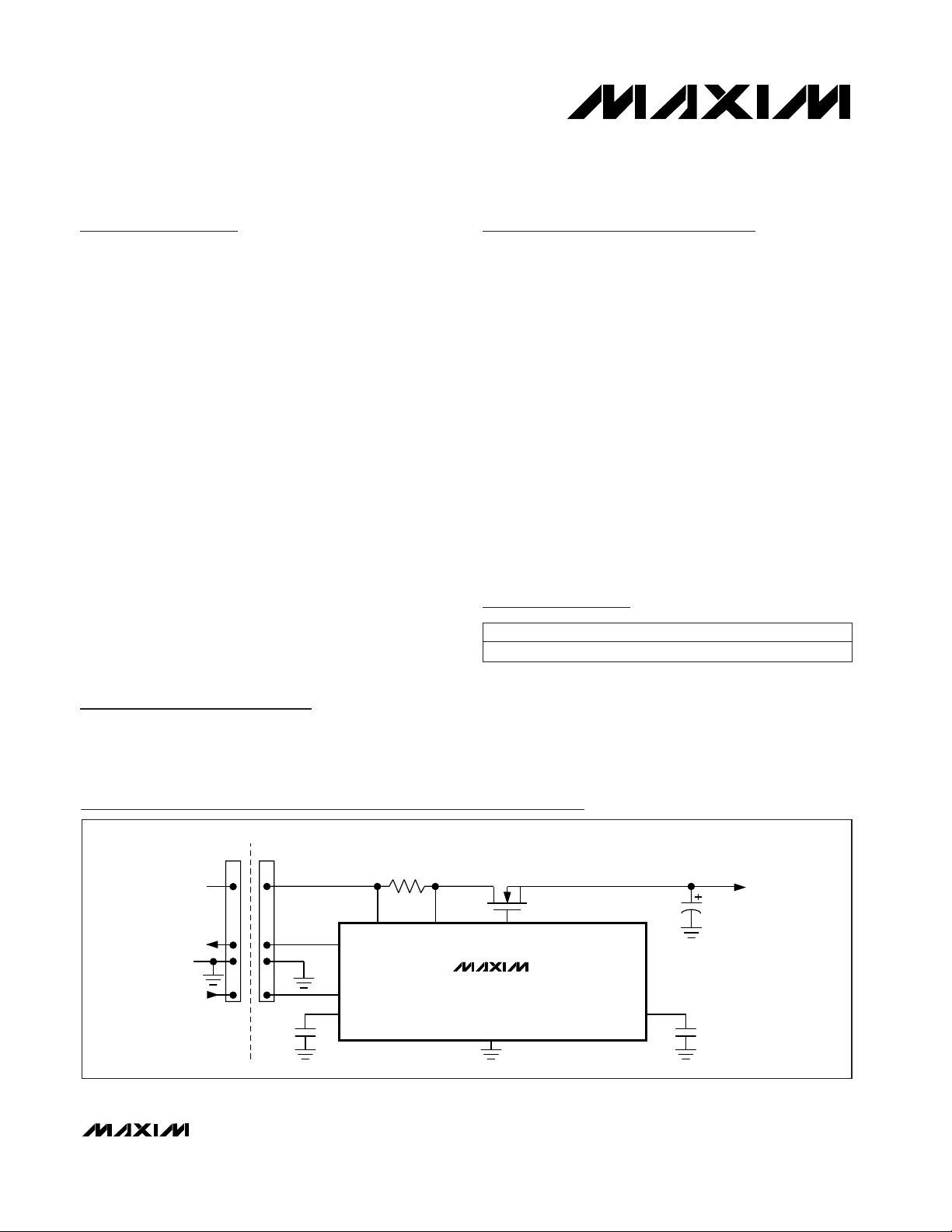
Typical Operating Circuit
19-1472; Rev 0; 4/99
PART
MAX4370ESA -40°C to +85°C
TEMP. RANGE PIN-PACKAGE
8 SO
Ordering Information
DualSpeed/BiLevel is a trademark of Maxim Integrated Products.
†
Patent Pending
Pin Configuration appears at end of data sheet.
Page 2
MAX4370
Current-Regulating Hot-Swap Controller with
DualSpeed/BiLevel Fault Protection
2 _______________________________________________________________________________________
ABSOLUTE MAXIMUM RATINGS
ELECTRICAL CHARACTERISTICS
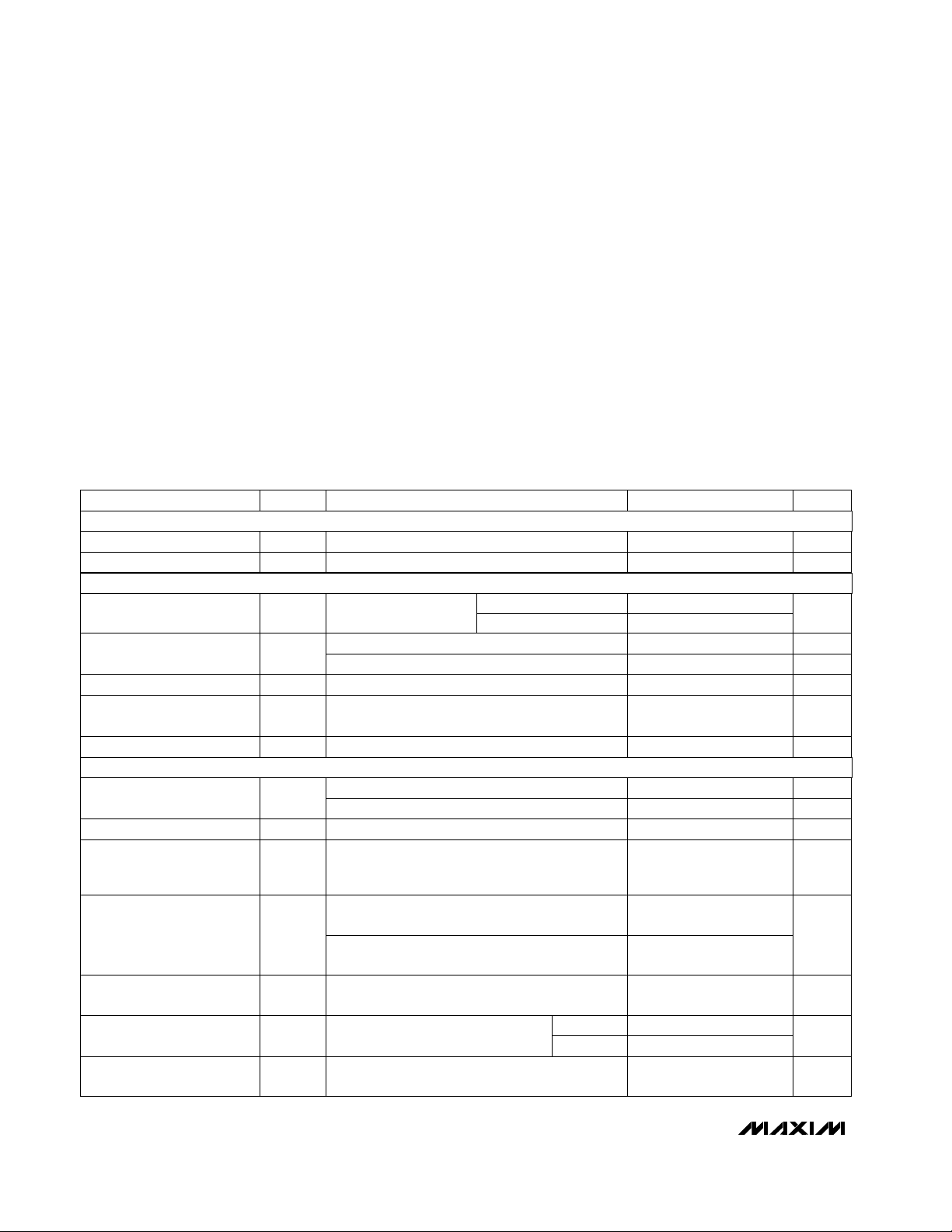
(VIN= +2.7V to +13.2V, TA= -40°C to +85°C, unless otherwise noted. Typical values are at VIN= +5V and TA= +25°C.) (Note 2)
Stresses beyond those listed under “Absolute Maximum Ratings” may cause permanent damage to the device. These are stress ratings only, and functional
operation of the device at these or any other conditions beyond those indicated in the operational sections of the specifications is not implied. Exposure to
absolute maximum rating conditions for extended periods may affect device reliability.
Note 1: ON can be pulled below ground. Limiting the current to 2mA ensures that this pin is never lower than about -0.8V.
V
IN
to GND...........................................................................+15V
STAT to GND..........................................................-0.3V to +14V
GATE to GND ..............................................-0.3V to (V
IN
+ 8.5V)
ON to GND (Note 1)................................................. -1V to +14V
CSPD to GND.............-0.3V to the lower of (V
IN
+ 0.3V) or +12V
VSEN, CTIM to GND....................................-0.3V to (V
IN
+ 0.3V)
Current into ON...................................................................±2mA
Current into Any Other Pin................................................±50mA
Continuous Power Dissipation (T
A
= +70°C)
SO (derate 5.9mW/°C above +70°C)........................... 471mW
Operating Temperature Range ...........................-40°C to +85°C
Storage Temperature Range.............................-65°C to +150°C
Lead Temperature (soldering, 10sec)............................ +300°C
Start-up is initiated only if V
GATE
is less than this
voltage
ON = V
IN
I
GATE
= 8.5µA, measured above V
IN
Measured with respect to VIN; voltage at which
internal clamp circuitry is triggered
During start-up (current regulation provided by
fast comparator)
Time from current overload to V
GATE
< 0.1V,
C
GATE
= 1000pF to GND (triggered by the fast
comparator during normal operation)
VSEN = V
IN
V
GATE
= VIN(Note 4)
CTIM = floating
10mV overdrive, from overload condition to GATE
discharging
VIN- VSEN
VIN- V
SEN
CSPD = floating
100nF on CTIM
100nF on CSPD to GND
CONDITIONS
V0.1Gate Overvoltage Threshold
V
2.7
5
Minimum Gate Drive Voltage
V6.7 7.5Maximum Gate Voltage
80
Gate Discharge Current
µs60t
OFF
Turn-Off Time
µA100I
GATE
Gate Charge Current
µs5.5
ms21 31 41
t
START
Start-Up Period
(Note 3)
mA0.6 1I
Q
Supply Current
V2.7 13.2V
IN
Input Voltage Range
µA0.2 10I
B,VSEN
VSEN Input Bias Current
ns460t
FCD
Fast Comparator Response
Time
mV180 200 220V
FC,TH
Fast Comparator Threshold
mV
45 50 55
V
SC,TH
Slow Comparator
Threshold
µs10 20 40
t
CSPD
Slow Comparator Response
Time
ms10 20 40
UNITSMIN TYP MAXSYMBOLPARAMETER
During turn-off, triggered by a fault in normal
operation or ON falling edge
µA
75 225 550
I
GATE,DIS
POWER SUPPLIES
MOSFET DRIVER
CURRENT CONTROL
VIN≥ 5V
VIN≥ 2.7V
TA= +25°C
TA= T
MIN
to T
MAX
43.5 56
Page 3
MAX4370
Current-Regulating Hot-Swap Controller with
DualSpeed/BiLevel Fault Protection
_______________________________________________________________________________________ 3
ELECTRICAL CHARACTERISTICS (continued)
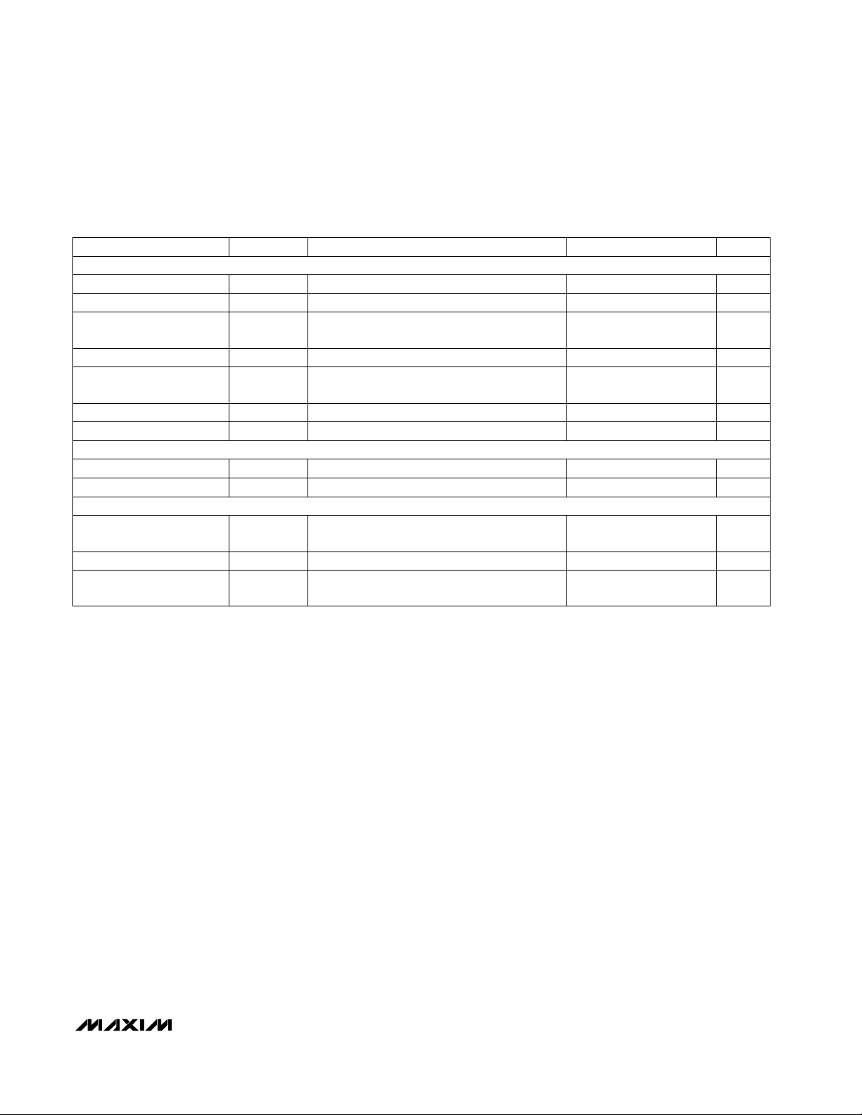
(VIN= +2.7V to +13.2V, TA= -40°C to +85°C, unless otherwise noted. Typical values are at VIN= +5V and TA= +25°C.) (Note 2)
Note 2: All devices are 100% tested at T
A
= +25°C. All temperature limits are guaranteed by design.
Note 3: The start-up period (t
START
) is the time during which the slow comparator is ignored and the device acts as a current limiter
by regulating the sense current with the fast comparator. It is measured from ON rising above 0.6V to STAT rising.
Note 4: The current available at GATE is a function of V
GATE
(see Typical
Operating Characteristics.
)
VIN= 5V, rising threshold
CONDITIONS
mV3V
HYST
Hysteresis
V0.575 0.6 0.625V
TH,ON
Threshold Voltage
UNITSMIN TYP MAXSYMBOLPARAMETER
2.7V ≤ VIN≤ 13.2V mV/V0.1 1PSRR
Power-Supply Rejection
Ratio
Input can be driven to the absolute maximum
limit without false output inversion
V-0.1 13.2
10mV overdrive
V
ON
Input Voltage Range
µs10t
D,COMP
Propagation Delay
µA0.001 1I
B,ON
Input Bias Current
To restart after a fault µs20t
RESTART
ON Pulse Width Low
V
STAT
≤ +13.2V µA1Output Leakage Current
I
SINK
= 1mA V0.4V
OL
Output Voltage Low
Start-up is initiated when this threshold is
reached at V
IN
V2.25 2.67V
UVLO
Threshold
mV100V
UVLO,HYST
Hysteresis
Time which input voltage must exceed undervoltage lockout before start-up is initiated
ms100 150 200t
D,UVLO
UVLO to Start-Up Delay
DIGITAL OUTPUT (STAT)
ON COMPARATOR
VINUNDERVOLTAGE LOCKOUT
Page 4
MAX4370
Current-Regulating Hot-Swap Controller with
DualSpeed/BiLevel Fault Protection
4 _______________________________________________________________________________________
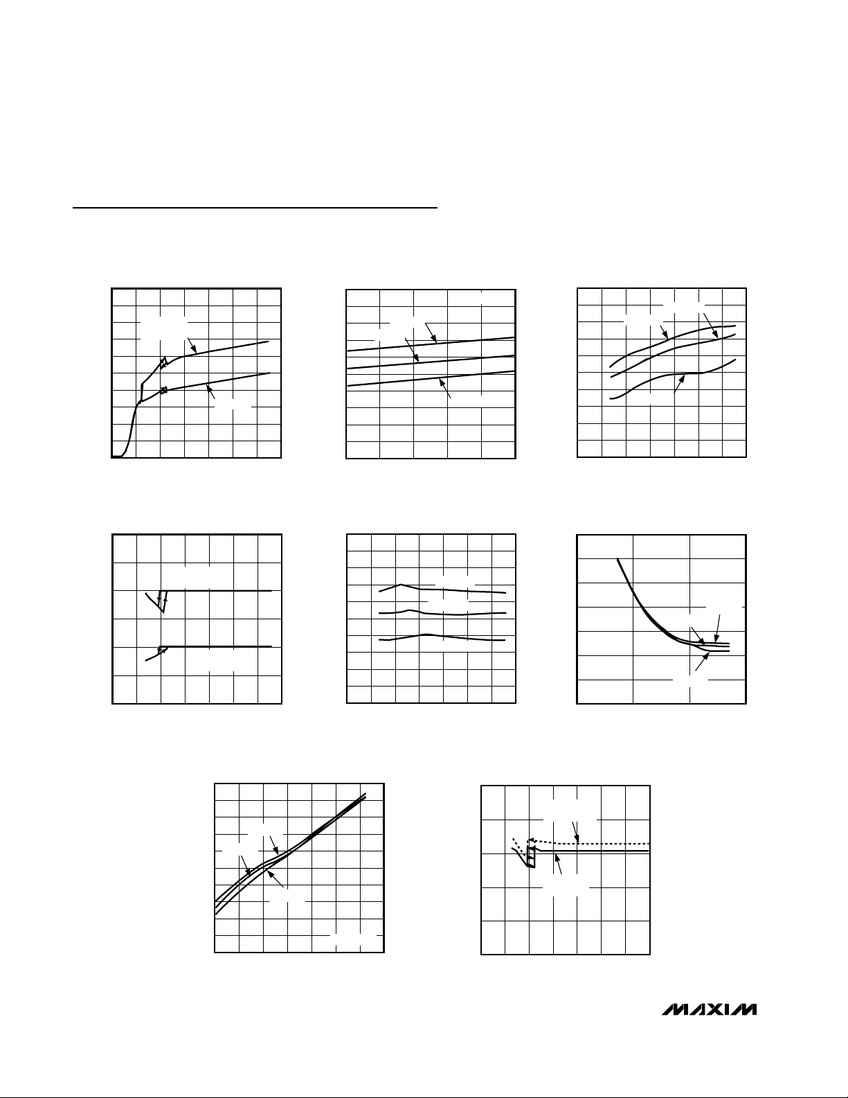
Typical Operating Characteristics
(Circuit of Figure 7, VIN= 5V, R
SENSE
= 100mΩ, M1 = FDS6670A, C
BOARD
= 470µF, C
GATE
= 0, RS= 0, TA= +25°C, unless other-
wise noted.)
0
0.3
0.2
0.1
0.5
0.4
0.9
0.8
0.7
0.6
1.0
02468101214
SUPPLY CURRENT vs. INPUT VOLTAGE
MAX4370 toc01
VIN (V)
SUPPLY CURRENT (mA)
ON = V
IN
I
GATE
= 10µA
ON = GND
-40 -15 10 35 60 85
SUPPLY CURRENT vs. TEMPERATURE
MAX4370 toc02
TEMPERATURE (°C)
0
0.3
0.2
0.1
0.5
0.4
0.9
0.8
0.7
0.6
1.0
SUPPLY CURRENT (mA)
ON = V
IN
VIN = 12V
VIN = 5V
VIN = 3V
49.0
49.6
49.4
49.2
50.0
49.8
50.8
50.6
50.4
50.2
51.0
02468101214
SLOW COMPARATOR THRESHOLD
vs. INPUT VOLTAGE
MAX4370 toc03
VIN (V)
V
SC, TH
(mV)
TA = -40°C
TA = +25°C
TA = +85°C
0
200
100
400
300
600
500
700
1 10 100 1000
FAST COMPARATOR RESPONSE TIME
vs. OVERDRIVE VOLTAGE
MAX4370 toc07
VOD (mV)
t
FCD
(ns)
VIN = 3V
VIN = 5V
VIN = 12V
18
20
19
22
21
23
24
18
20
19
22
21
23
24
0682 4 10 12 14
SLOW COMPARATOR
RESPONSE TIME vs. INPUT VOLTAGE
MAX4370 toc05
VIN (V)
t
CSPD
(µs)
t
CSPD
(ms)
CSPD = 110nF
TIME IN ms
CSPD = 0
TIME IN µs
190
196
194
192
200
198
108
206
204
202
210
FAST COMPARATOR THRESHOLD
vs. INPUT VOLTAGE
MAX4370 toc06
V
FC, TH
(mV)
02468101214
V
IN
(V)
TA = -40°C
TA = +25°C
TA = +85°C
400
430
420
410
450
440
490
480
470
460
500
-40 -20 0 20 40 60 80 100
FAST COMPARATOR RESPONSE TIME
vs. TEMPERATURE
MAX4370 toc08
TEMPERATURE (°C)
t
FCD
(ns)
VIN = 12V
VIN = 3V
VOD = 10mV
VIN = 5V
250
270
310
290
330
350
042 6 8101214
START-UP TIME
vs. INPUT VOLTAGE
MAX4370 toc09
VIN (V)
t
START
(µs)
25
27
31
29
33
35
t
START
(ms)
C
TIM
= 100nF
TIME IN ms
C
TIM
= 1nF
TIME IN µs
Page 5
MAX4370
Current-Regulating Hot-Swap Controller with
DualSpeed/BiLevel Fault Protection
_______________________________________________________________________________________
5
0
60
40
20
80
100
120
0862 4 10 12 14 16 18 20
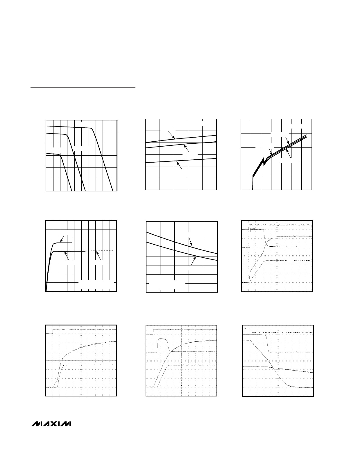
GATE CHARGE CURRENT
vs. GATE VOLTAGE
MAX4370 toc10
V
GATE
(V)
I
GATE
(µA)
VIN = 12V
VIN = 5.0V
VIN = 3.0V
0
50
25
100
75
125
150
-40 -10 35-15 60 85
GATE CHARGE CURRENT
vs. TEMPERATURE
MAX4370 toc11
TEMPERATURE (°C)
I
GATE
(µA)
VIN = 12V
V
GATE
= 0
VIN = 5V
VIN = 3V
0
5
15
10
20
25
042 6 8101214
GATE VOLTAGE vs. INPUT VOLTAGE
MAX4370 toc12
VIN (V)
V
GATE
(V)
I
GATE
= 10µA
TA = +85°C
TA = +25°C
TA = -40°C
0
100
50
150
300
350
250
200
400
0 468102 1214161820
GATE DISCHARGE CURRENT
vs. GATE VOLTAGE
MAX4370 toc13
V
GATE
(V)
I
GATE
(µA)
VIN = 12V
VIN = 3V
TRIGGERED BY A FAULT
OR BY ON FALLING
VIN = 5V
C
BOARD
= 0, R
SENSE
= 100mΩ,
C
TIM
= 10nF, C
GATE
= 0
V
OUT
(2V/div)
V
GATE
(2V/div)
ON
100µs/div
START-UP TIME (C
BOARD
= 0)
MAX4370-16
0
100
50
200
150
350
300
250
400
-40 10-15 35 60 85
GATE DISCHARGE CURRENT
vs. TEMPERATURE
MAX4370 toc14
TEMPERATURE (°C)
I
GATE
(µA)
VIN = 3V
VIN = 5V & 12V
V
GATE
= V
IN
TRIGGERED BY A FAULT
OR BY ON FALLING
C
BOARD
= 470µF, R
SENSE
= 100mΩ,
C
TIM
= 10nF, C
GATE
= 0
I
LOAD
(1A/div)
V
OUT
(2V/div)
V
GATE
(2V/div)
ON
500µs/div
START-UP TIME (C
BOARD
= 470µF)
MAX4370-15
C
BOARD
= 470µF, R
SENSE
= 100mΩ,
C
GATE
= 22nF, C
TIM
= 10nF, RS = 0
I
LOAD
(1A/div)
V
OUT
(2V/div)
V
GATE
(2V/div)
ON
1ms/div
START-UP TIME
(EXTERNAL C
GATE
= 22nF, C
BOARD
= 470µF)
MAX4370-17
C
BOARD
= 470µF, R
SENSE
= 100mΩ,
C
GATE
= 0
I
LOAD
(1A/div)
V
OUT
(2V/div)
V
GATE
(2V/div)
0A
50µs/div
TURN-OFF TIME (C
BOARD
= 470µF)
MAX4370-18
ON
0V
Typical Operating Characteristics (continued)
(Circuit of Figure 7, VIN= 5V, R
SENSE
= 100mΩ, M1 = FDS6670A, C
BOARD
= 470µF, C
GATE
= 0, RS= 0, TA= +25°C, unless other-
wise noted.)
Page 6
MAX4370
Current-Regulating Hot-Swap Controller with
DualSpeed/BiLevel Fault Protection
6 _______________________________________________________________________________________
Typical Operating Characteristics (continued)
(Circuit of Figure 7, VIN= 5V, R
SENSE
= 100mΩ, M1 = FDS6670A, C
BOARD
= 470µF, C
GATE
= 0, RS= 0, TA= +25°C, unless other-
wise noted.)
C
BOARD
= 0, R
SENSE
= 100mΩ,
C
GATE
= 0, RS = 0
I
LOAD
(1A/div)
V
OUT
(2V/div)
V
GATE
(2V/div)
0
50µs/div
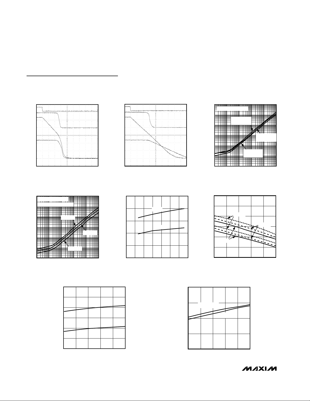
TURN-OFF TIME (C
BOARD
= 0)
MAX4370-19
ON
A
0V
C
BOARD
= 470µF, R
SENSE
= 100mΩ,
C
GATE
= 22nF, RS = 0
I
LOAD
(1A/div)
V
OUT
(2V/div)
V
GATE
(2V/div)
0A
0V
200µs/div
TURN-OFF TIME
(EXTERNAL C
GATE
= 22nF, C
BOARD
= 470µF)
MAX4370-20
ON
0.01 0.1 1 10 100 1000
TIME TO CHARGE GATE
vs. C
GATE
MAX4370 toc21
C
GATE
(nF)
TIME TO CHARGE GATE (ms)
1000
0.001
0.01
1
0.1
100
10
NO EXTERNAL MOSFET
VIN = 12V
TO V
GATE
= 17V
VIN = 5V
TO V
GATE
= 10V
VIN = 3V
TO V
GATE
= 6V
0.01 0.1 1 10 100 1000
TIME TO DISCHARGE GATE
vs. C
GATE
MAX4370 toc22
C
GATE
(nF)
TIME TO DISCHARGE GATE (ms)
1000
0.001
1
0.1
0.01
10
100
VIN = 12V
VIN = 5V
VIN = 3V
DISCHARGE TO V
GATE
=0.1V
NO EXTERNAL MOSFET
0.595
0.597
0.601
0.599
0.603
0.605
042 6 8101214
ON COMPARATOR THRESHOLD
vs. INPUT VOLTAGE
MAX4370 toc23
VIN (V)
ON COMPARATOR THRESHOLDD (V)
RISING
FALLING
0.5950
0.6000
0.5975
0.6050
0.6025
0.6075
0.6100
-40 35 60-15 10 85
ON COMPARATOR THRESHOLD
vs. TEMPERATURE
MAX4370 toc24
TEMPERATURE (°C)
ON COMPARATOR THRESHOLD (V)
RISING
FALLING
}
}
VIN = 12V
VIN = 5V
VIN = 3V
2.30
2.40
2.35
2.50
2.45
2.55
2.60
-40 35 60-15 10 85
UVLO THRESHOLD VOLTAGE
vs. TEMPERATURE
MAX4370 toc25
TEMPERATURE (°C)
UVLO THRESHOLD (V)
RISING
FALLING
140
145
150
155
160
UVLO DELAY vs. TEMPERATURE
MAX4370 toc26
TEMPERATURE (°C)
UVLO DELAY (ms)
-40 35 60-15 10 85
VIN = 3V
VIN = 5V & 12V
Page 7
MAX4370
Current-Regulating Hot-Swap Controller with
DualSpeed/BiLevel Fault Protection
_______________________________________________________________________________________ 7
Pin Description
PIN
Supply Voltage Input. Connect to 2.7V to 13.2V.V
IN
1
FUNCTIONNAME
Current-Sense Resistor Voltage Input. R
SENSE
is connected from VINto VSEN.VSEN2
GroundGND4
Gate Drive Output. Connect to gate of external N-channel MOSFET.GATE3
Start-Up Timer Setting. Leave floating or connect the timing capacitor from CTIM to GND. See
Start-Up
Timing Capacitor
section.
CTIM6
ON Comparator Input. Connect high for normal operation; connect low to force the MOSFET off. Comparator
threshold V
TH,ON
= 0.6V allows for precise control over shutdown feature. Pulse ON low for at least 20µs,
then high to restart after a fault.
ON8
Status Output—open drain. High indicates start-up completed with no fault. See Table 1.STAT7
Slow Comparator Speed Setting. Leave floating or connect the timing capacitor from CSPD to GND. See
Slow Comparator Response Time
section.
CSPD5
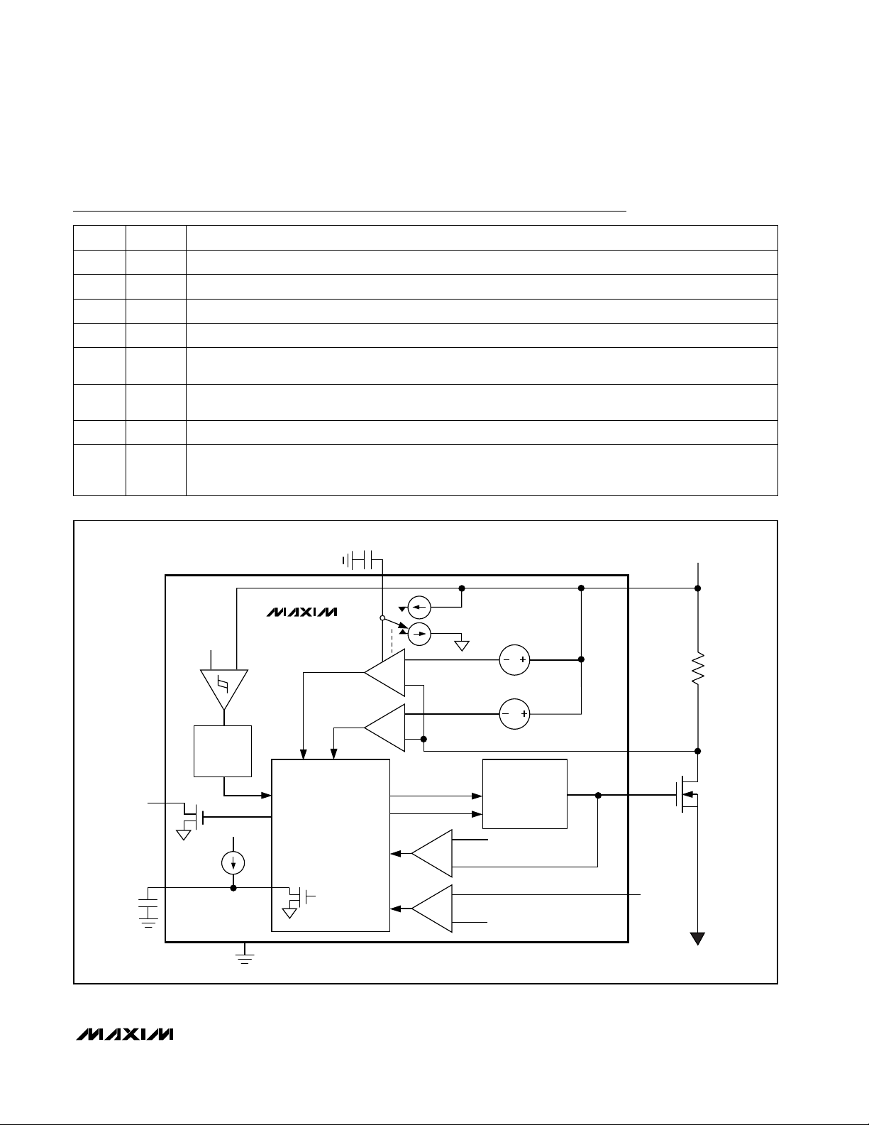
Figure 1. Functional Diagram
C
SPD
2.45V
INPUT
UVLO
MAX4370
SLOW COMPARATOR
FAST COMPARATOR
CSPD
6µA
6µA
V
SC, TH
50mV
V
FC, TH
200mV
V
IN
R
SENSE
STAT
CTIM
C
TIM
150ms
DELAY
ON
VIN RISING
V
VSEN
GATE
DISCHARGE
LOGIC
CONTROL
IN
4µA
GND
ENABLE
DRIVE
CHARGE
PUMP
0.1V
GATE
OVLO
ON COMPARATOR
0.6V
GATE
ON
M1
N
V
OUT
Page 8
MAX4370
Current-Regulating Hot-Swap Controller with
DualSpeed/BiLevel Fault Protection
8 _______________________________________________________________________________________
Detailed Description
The MAX4370 is a circuit-breaker IC designed for hotswap applications where a card or board is to be
inserted into a rack with the main system power supply
turned on. Normally, when a card is plugged into a live
backplane, the card is discharged filter capacitors provide a low impedance, which can momentarily cause
the main power supply to collapse. The MAX4370 is
designed to reside either in the backplane or in the
removable card to provide inrush-current limiting and
short-circuit protection. This is achieved using a charge
pump as gate drive for an external N-channel MOSFET,
an external current-sense resistor, and two on-chip
comparators. Figure 1 shows the device’s functional
diagram.
The slow comparator response time and the start-up
timer can be adjusted with external capacitors. The timing components are optional; without them the part is
set to its nominal values, as shown in the
Electrical
Characteristics.
Start-Up Period
CTIM sets the start-up period. This mode starts when
the power is first applied to VINif ON is connected to
VIN, or at the rising edge of ON. In addition, the voltage
at VINmust be above the undervoltage lockout for
150ms (see
Undervoltage Lockout
).
During start-up, the slow comparator is disabled and
current limiting is provided two different ways:
1) Slow ramping of the current to the load by controlling
the external MOSFET gate voltage.
2) Limiting the current to the load by regulating the voltage across the external current-sense resistor.
Unlike other circuit-breaker ICs, the MAX4370 hot-swap
controller regulates the current to a preset level instead
of completely turning off if an overcurrent occurs during
start-up.
In start-up mode, the gate drive current is limited to
100µA and decreases with the increase of the gate
voltage (see
Typical Operating Characteristics
). This
allows the MAX4370 to slowly enhance the MOSFET. If
the fast comparator detects an overcurrent, the gate
voltage is momentarily discharged with a fixed 80µA
current until the load current through the sense resistor
(R
SENSE
) decreases below its threshold point. This
effectively regulates the turn-on current during start-up.
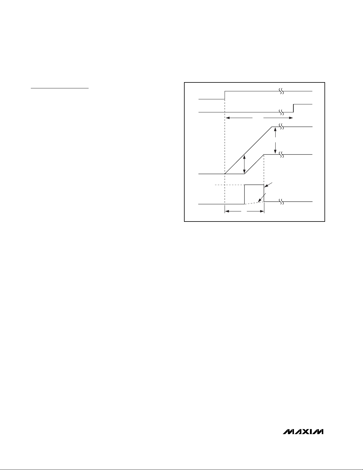
Figure 2 shows the start-up waveforms. STAT goes
high at the end of the start-up period if no fault condition is present.
Normal Operation (DualSpeed/BiLevel)
In normal operation (after the start-up period has
expired), protection is provided by turning off the external MOSFET when a fault condition is encountered.
DualSpeed/BiLevel fault protection incorporates two
comparators with different thresholds and response
times to monitor the load current:
1) Slow Comparator. This comparator has an externally
set response time (20µs to seconds) and a fixed
50mV threshold voltage. The slow comparator
ignores low-amplitude momentary current glitches.
After an extended overcurrent condition, a fault is
detected and the MOSFET gate is discharged.
2) Fast Comparator. This comparator has a fixed
response time and a higher 200mV threshold voltage. The fast comparator turns off the MOSFET
immediately after it detects a large amplitude event
such as a short circuit.
In each case, when a fault is encountered, the status
pin (STAT) goes low and the MAX4370 stays latched
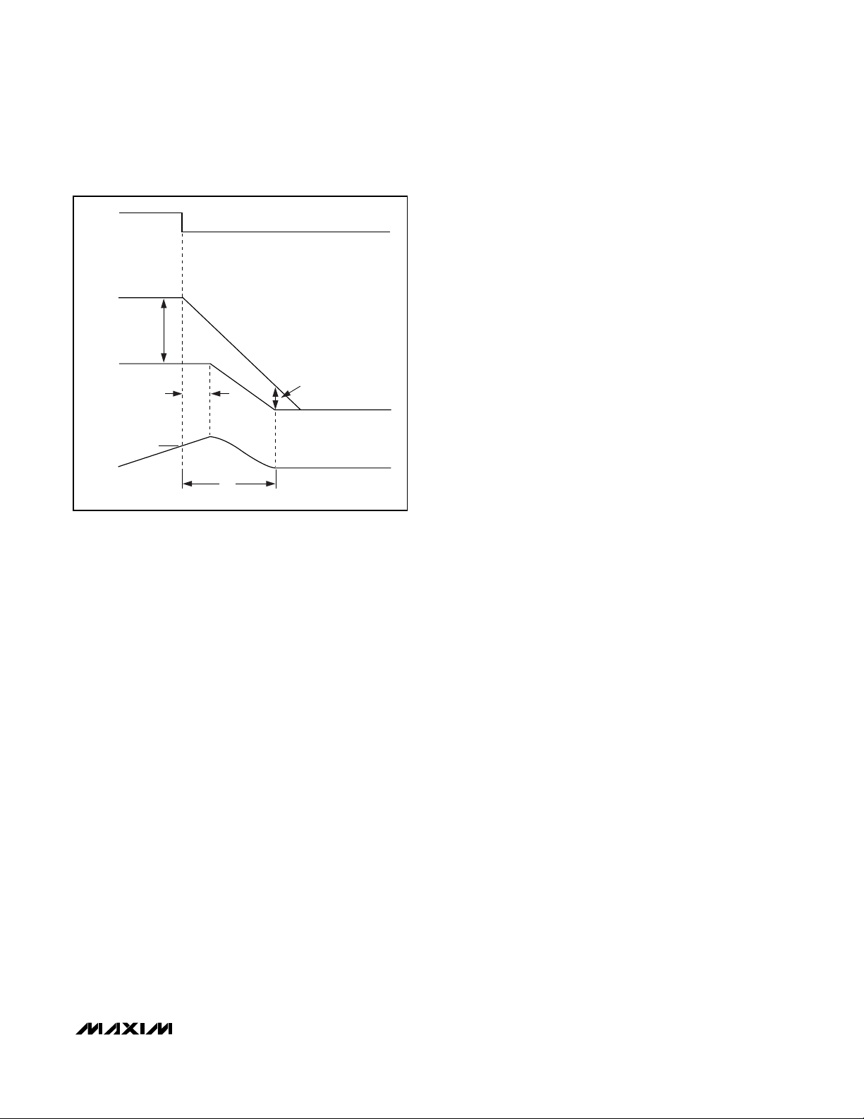
off. Figure 3 shows the waveforms after a fault condition.
t
START
t
ON
~V
IN
V
GATE
I
FAST, SET
V
GATE
STAT
ON
V
TH
V
OUT
C
BOARD
= LARGE
C
BOARD
= 0
V
OUT
I
LOAD
Figure 2. Start-Up Waveforms
Page 9
MAX4370
Current-Regulating Hot-Swap Controller with
DualSpeed/BiLevel Fault Protection
_______________________________________________________________________________________ 9
Slow Comparator
The slow comparator is disabled at start-up while the
external MOSFET is turning on. This allows the part to
ignore the higher-than-normal inrush current charging
the board capacitors (C
BOARD
) when a card is first
plugged in.
If the slow comparator detects an overload current
while in normal operation (after start-up is completed),
it turns off the external MOSFET by discharging the
gate capacitance with a 200µA current. The slow comparator threshold is set at 50mV and has a default
delay of 20µs (CSPD floating), allowing it to ignore
power-supply glitches and noise. The response time
can be lengthened with an external capacitor at CSPD
(Figure 8).
If the overcurrent condition is not continuous, the duration above the threshold minus the duration below it
must be greater than 20µs (or the external programmed
value) for the device to trip. When the current is above
the threshold, CSPD is charged with a 6µA current
source; when the current is below the threshold, CSPD
is discharged with a 6µA current source. A fault is
detected when CSPD is charged to the trip point of
1.2V. A pulsing current with a duty cycle greater than
50% (i.e., > 50% of the time the current is above the
threshold level) will be considered a fault condition
even if it is never higher than the threshold for more
than the slow comparator’s set response time.
Once the fault condition is detected, the STAT pin goes
low and the device goes into latched mode. The GATE
voltage discharge rate depends on the gate capacitance and the external capacitance at GATE.
Fast Comparator
The fast comparator behaves differently according to
the operating mode. During start-up, the fast comparator is part of a simple current regulator. When the
sensed current is above the threshold (V
FC,TH
=
200mV), the gate is discharged with a 80µA current
source. When the sensed current drops below the
threshold, the charge pump turns on again. The sensed
current will rise and fall near the threshold due to the
fast comparator and charge-pump propagation delay.
The gate voltage will be roughly saw-tooth shaped, and
the load current will present a 20% ripple. The ripple
can be reduced by adding a capacitor from GATE to
GND. Once C
BOARD
is completely charged, the load
current drops to its normal operating levels. If the
sensed current is still high after the start-up timer
expires, the MOSFET gate is discharged completely.
In normal operation (after start-up), the fast comparator
is used as an emergency off switch. If the load current
reaches the fast comparator threshold, the device
immediately forces the MOSFET off completely by discharging the GATE with a 200µA current. This can
occur in the event of a serious current overload or a
dead short. Given a 1000pF gate capacitance and 12V
gate voltage, the MOSFET will be off in less than 60µs.
Any additional capacitance connected between GATE
and GND to slow down the turn-on time also increases
the turn-off time.
Latched Mode and Reset
The MOSFET driver of the MAX4370 stays latched off
after a fault condition until it is reset by a negativegoing pulse on the ON pin. Pulse ON low for 20µs
(min), then high to restart after a fault. During start-up, a
negative-going edge on ON will force the device to turn
off the MOSFET and place the device in latched mode.
Keep ON low for 20µs (min) to restart.
t
OFF
V
GATE
STAT
~V
TH
~V
IN
V
OUT
I
LOAD
I
LIM
t
d
Figure 3. Response to a Fault Condition
Page 10
MAX4370
Current-Regulating Hot-Swap Controller with
DualSpeed/BiLevel Fault Protection
10 ______________________________________________________________________________________
Status Output
The status output is an open-drain output that goes low
when the part is:
1) in start-up
2) forced off (on = GND)
3) in an overcurrent condition, or
4) latched off.
STAT is high only if the part is in normal mode and no
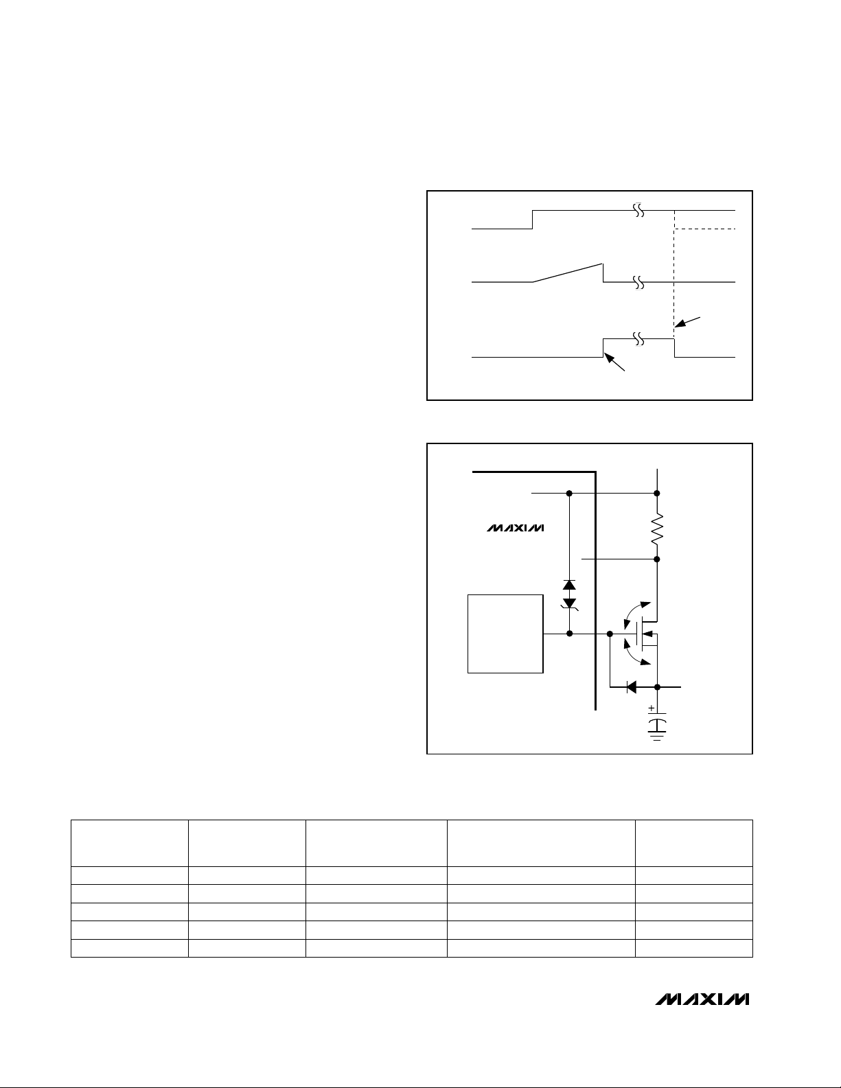
faults are present (Table 1). Figure 4 shows the STAT
timing diagram.
Over/Undervoltage Lockouts
The undervoltage lockout prevents the MAX4370 from
turning on the external MOSFET until the input voltage
at VINexceeds the lockout threshold (2.25V min) for at
least 150ms. The undervoltage lockout protects the
external MOSFET from insufficient gate drive voltage.
The 150ms timeout ensures that the board is fully
plugged into the backplane and that VINis stable.
Voltage transients at VINwith voltages below the UVLO
will reset the device and initiate a start-up sequence.
The device also features a gate overvoltage lockout
that prevents the device from restarting after a fault
condition if the discharge has not been completed.
V
GATE
must be discharged to below 0.1V before
restarting. Since the MAX4370 does not monitor the
output voltage, a start-up sequence can be initiated
while the board capacitance is still charged.
Gate Overvoltage Protection
Newer-generation MOSFETs have an absolute maximum rating of ±8V for the gate-to-source voltage (VGS).
To protect these MOSFETs, the MAX4370 limits the
gate-to-drain (VGD) to +7.5V with an internal zener
diode. No protection is provided for negative VGD. If
GATE can be discharged to GND faster than the output
voltage, an external small-signal protection diode (D1)
can be used, as shown in Figure 5.
Table 1. Status Output Truth Table
PART IN
START-UP
XYes
ON PIN
OVERCURRENT
CONDITION ON V
IN
XX
PART IN LATCHED-OFF MODE
DUE TO OVERCURRENT
CONDITION
Low
STAT PIN
(STATUS)
XX LowLowNo
XYes Low
YesNo LowHighNo
HighNo
NoNo HighHighNo
Figure 4. Status Output (STAT) Timing Diagram
D1
GATE
R
SENSE
V
OUT
V
GD
V
GS
C
BOARD
V
IN
V
SEN
M1
N
MAX4370
GATE DRIVE
CHARGE PUMP
Figure 5. External Gate-Source Protection
X = Don’t care
V
IN
ON
OV
1.2V
CTIM
OV
V
IN
STAT
OV
NO FAULT CONDITIONS
PRESENT
FAULT
CONDITION
OR ON
FALLING EDGE
Page 11
MAX4370
Current-Regulating Hot-Swap Controller with
DualSpeed/BiLevel Fault Protection
______________________________________________________________________________________ 11
__________Applications Information
Component Selection
N-Channel MOSFET
Select the external N-channel MOSFET according to
the application’s current level. The MOSFET’s R
DS(ON)
should be chosen low enough to have a minimum voltage drop at full load to limit the MOSFET power dissipation. High R
DS(ON)
can cause output ripple if the board
has pulsing loads, or it can trigger an external undervoltage reset monitor at full load. Determine the
device’s power rating requirement to accommodate a
short-circuit condition on the board during start-up (see
MOSFET Thermal Considerations
).
MOSFETs can typically withstand single-shot pulses
with higher dissipation than the specified package rating. Also, since part of the inrush current limiting is
achieved by limiting the gate dV/dt, it is not necessary
to use a MOSFET with low gate capacitance. Table 2
lists some recommended manufacturers and components.
Sense Resistor
The slow comparator threshold voltage is set at 50mV.
Select a sense resistor that causes a 50mV voltage
drop at a current level above the maximum normal
operating current. Typically, set the overload current at
1.2 to 1.5 times the nominal load current. The fast comparator threshold is set at 200mV. This sets the fault
current limit at four times the overload current limit.
Choose the sense-resistor power rating to accommodate the overload current (Table 3):
P
SENSE
= (I
OVERLOAD
)2· R
SENSE
Start-Up Timing Capacitor (C
TIM
)
The start-up period (t
START
) is determined by the capacitor connected at CTIM. This determines the maximum
time allowed to completely turn on the MOSFET.
The default value for t
START
is chosen by leaving CTIM
floating and is approximately 5.5µs. This is also the
minimum value (not controlled and dependent on stray
capacitance). Longer timings are determined by the
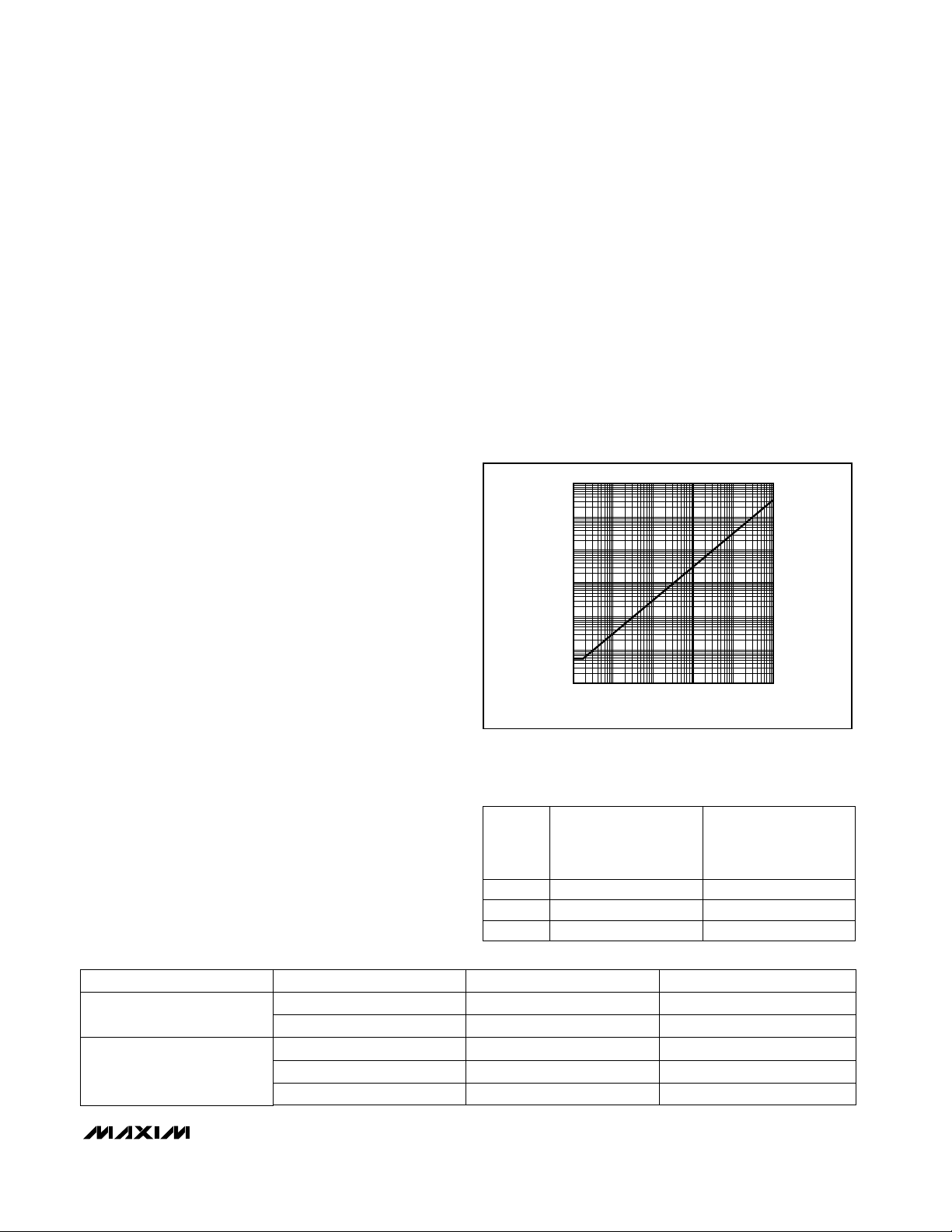
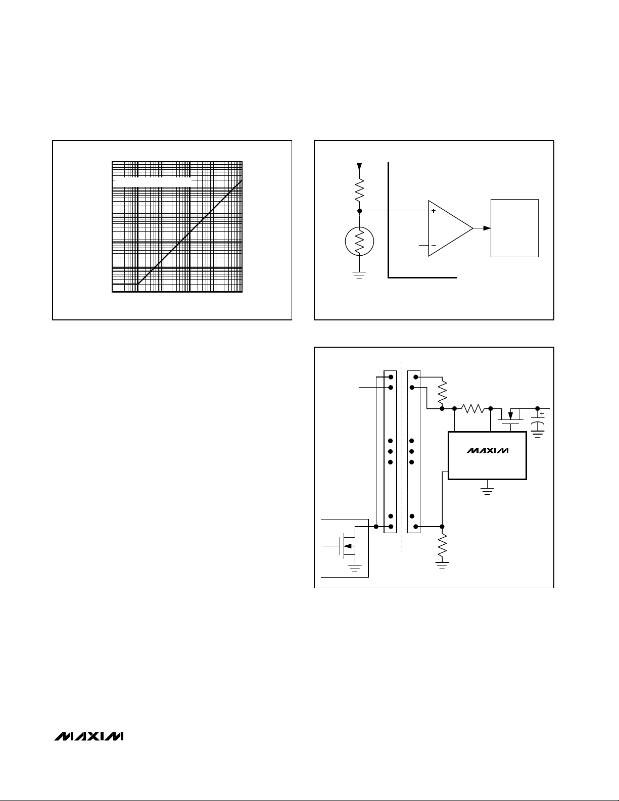
value of the capacitor, according to Figure 6, and can
be determined as follows:
t
START
(ms) = 0.31 · C
TIM
(nF)
Set the t
START
timer to allow the MOSFET to be
enhanced and the load capacitor to be completely
charged.
There are two methods of completing the start-up
sequences. Case A describes a start-up sequence that
does not use the current-limiting feature and slowly turns
on the MOSFET by limiting the gate dV/dt. Case B uses
the current-limiting feature and turns on the MOSFET as
fast as possible while still preventing high inrush current.
0.01 0.1 1 10 100 1000
CAPACITANCE (nF)
t
START
(ms)
1000
0.1
0.01
0.001
1
10
100
Figure 6. Start-Up Period vs. C
TIM
Table 3. Current Levels vs. R
SENSE
150
0.5100
R
SENSE
(mΩ)
510
OVERLOAD
THRESHOLD SET BY
SLOW COMPARATOR
(A)
4
2
20
FAULT CURRENT
THRESHOLD SET BY
FAST COMPARATOR
(A)
Table 2. Component Manufacturers
704-264-8861
888-522-5372
402-564-3131
PHONE
www.irctt.co
www.fairchildsemi.com
www.vishay.com
INTERNET
310-322-3331
IRC
Sense Resistors
602-244-3576
www.irf.com
www.mot-sps.com/ppd/
International Rectifier
Motorola
Fairchild
COMPONENT
Dale-Vishay
MANUFACTURER
MOSFETs
Page 12
MAX4370
Current-Regulating Hot-Swap Controller with
DualSpeed/BiLevel Fault Protection
12 ______________________________________________________________________________________
Case A: Slow Turn-On (without overcurrent)
There are two ways to turn on the MOSFET without
reaching the fast comparator current limit:
1) If the board capacitance (C
BOARD
) is low, the
inrush current is low.
2) If the capacitance at GATE is high, the MOSFET
turns on slowly.
In both cases, the turn-on (tON) is determined only by
the charge required to enhance the MOSFET—effectively, the small gate-charging current limits the output
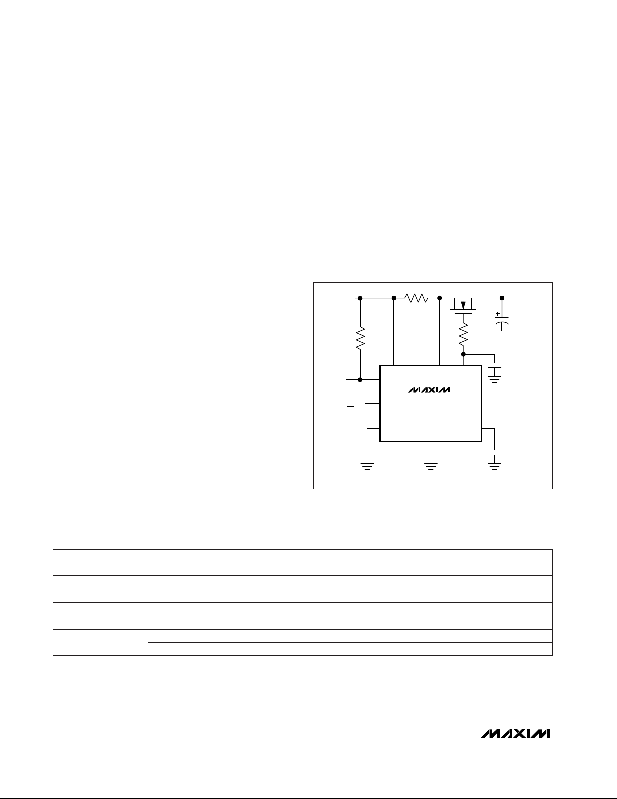
voltage dv/dt. This time can be extended by connecting an external capacitor between GATE and GND, as
shown in Figure 7. The turn-on time is dominated by the
external gate capacitance if its value is considerably
higher than MOSFET gate capacitance. Table 4 shows
the timing required to enhance the recommended
MOSFET with or without an external capacitor at GATE;
Figures 2 and 3 show the related waveforms and timing
diagrams (see Start-Up Time with C
BOARD
= 0 and
Start-Up Time with External C
GATE
in the
Typical
Operating Characteristics
). Remember that a high gate
capacitance also increases the turn-off time.
When using the MAX4370 without an external gate
capacitor, RSis not necessary. RSprevents MOSFET
source oscillations that can occur when C
GATE
is high
while C
BOARD
is low.
Case B: Fast Turn-On (with current limit)
In applications where the board capacitor (C
BOARD
) at
V
OUT
is high, the inrush current causes a voltage drop
across R
SENSE
that exceeds the fast comparator
threshold (V
FC,TH
= 200mV). In this case, the current
charging C
BOARD
can be considered constant and the
turn-on time is determined by:
tON= C
BOARD
· VIN/ I
FAST,SET
where the maximum load current I
FAST,SET
= V
FC,TH
/
R
SENSE
. Figure 2 shows the waveforms and timing diagrams for a turn-on transient with current regulation (see
Start-Up Time with C
BOARD
= 470µF in the
Typical
Operating Characteristics
). When operating under this
condition, an external gate capacitor is not required.
Adding an external capacitor at GATE reduces the regulated current ripple but increases the turn-off time by
increasing the gate delay (td) (Figure 3).
M1
C
SPD
*OPTIONAL (SEE TEXT)
C
TIM
CTIM
GATE
VSEN
GND
CSPD
ON
R
SENSE
V
OUT
C
GATE
C
BOARD
V
IN
V
IN
R
S*
MAX4370
R
PULL-UP
STAT
Figure 7. Operation with External Gate Capacitor
Table 4. MOSFET Turn-On Time (start-up without current limit)
(C
BOARD
= 0, turn-on with no load current, turn-off with 2A fault current)
International Rectifier
IRF7401
Fairchild FDS6670A
0
22
0
175µs
1.9ms
220µs
130µs
1.8ms
160µs
160µs
3.5ms
MOSFET TURN-ON (tON)
190µs
75µs
540µs
70µs
130µs
1.1ms
130µs
160µs
2ms
MOSFET TURN-OFF (t
OFF
)
145µs
22 2.3ms 2ms 3.2ms 540µs 1.1ms 1.95ms
0
22
101µs
2ms
74µs
1.8ms
Motorola
MMSF5N03HD
73µs
3.2ms
33µs
470µs
67µs
1ms
85µs
1.95ms
C
GATE
(nF)
VIN= 3V VIN= 5V VIN= 12V VIN= 3V VIN= 5V VIN= 12V
DEVICE
Electrical characteristics as specified by the manufacturer’s data sheet:
FDS6670A: C
ISS
= 3200pF, Q
T(MAX)
= 50nC, R
DS(ON)
= 8.2mΩ
IRF7401: C
ISS
= 1600pF, Q
T(MAX)
= 48nC, R
DS(ON)
= 22mΩ
MMSF5N03HD: C
ISS
= 1200pF, Q
T(MAX)
= 21nC, R
DS(ON)
= 40mΩ
Page 13
The actual turn-on time is determined by the longer of
the two timings of Case A and Case B. Set the start-up
timer (t
START
) at 2 · tONor longer to guarantee enough
time for the output voltage to settle; also take into consideration device parameter variation.
Slow Comparator Response Time (C
SPD
)
The slow comparator threshold is set at 50mV, and its
response time is determined by the external capacitor
connected to CSPD (Figure 8).
A minimum response time of 20µs (typ) is achieved by
leaving this pin floating. This time is determined internally and is not affected by stray capacitance at CSPD
(up to 100pF).
Set the slow comparator response time to be longer
than the normal operation load transients.
ON Comparator
The ON/OFF function of the MAX4370 is controlled by
the ON comparator. This is a precision voltage comparator that can be used for temperature monitoring
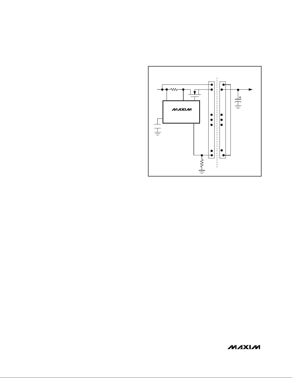
(Figure 9) or as an additional undervoltage lockout. The
comparator threshold voltage is set at 0.6V with a 3mV
typical hysteresis.
The ON comparator initiates start-up when its input voltage (VON) rises above the threshold voltage, and turns
off the MOSFET when the voltage falls below the
threshold. The ON comparator is also used to reset the
MAX4370 after a fault condition.
The ON comparator input and the STAT output can be
pulled to voltages up to 14V independently of VIN.
In some applications, it is useful to use connectors with
staggered leads. In Figure 10, the ON pin forces the
removable board to be powered up only when all connections are made.
MAX4370
Current-Regulating Hot-Swap Controller with
DualSpeed/BiLevel Fault Protection
______________________________________________________________________________________ 13
0.01 0.1 1 10 100 1000
C
SPD
(nF)
RESPONSE TIME (ms)
1000
0.1
0.01
1
10
100
t
CSPD
(ms) = 0.2 · C
SPD
(nF)
Figure 8. Slow Comparator Response Time vs. C
SPD
LOGIC
CONTROL
V
REF
R2
ON
NTC
R1 = R2
· (V
REF
/ O.6 - 1)
R2 = VALUE OF THE NTC RESISTOR AT THE LIMIT TEMPERATURE
V
REF
= ANY REFERENCE VOLTAGE AVAILABLE OR V
IN
0.6V
R1
Figure 9. Temperature Monitoring and Protection
V
IN
ON
BACKPLANE
10k
1M
RESET
V
CC
MAX4370
VSEN
GATE
REMOVABLE
CARD
Figure 10. Fail-Safe Connector
Page 14
MAX4370
Using the MAX4370 on the Backplane
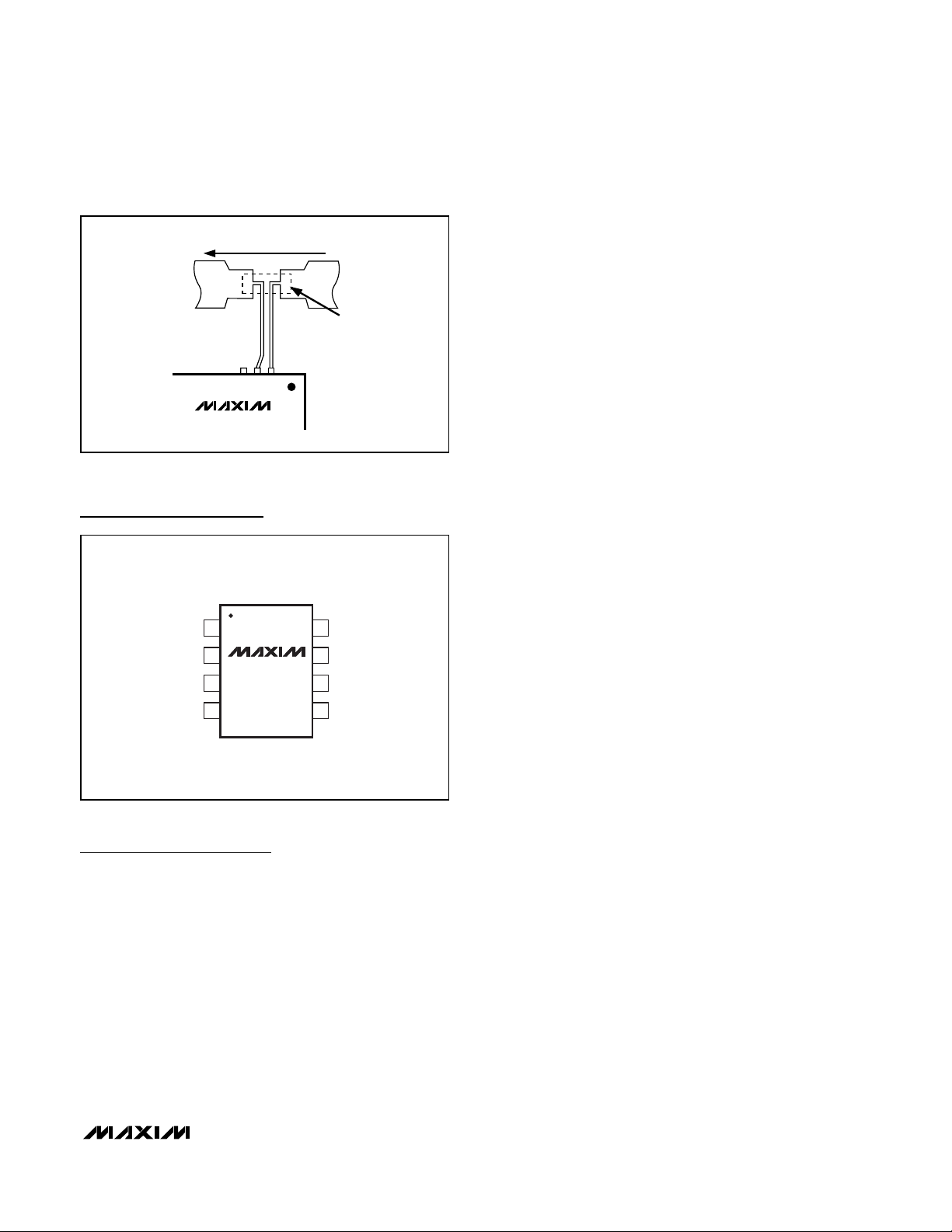
The MAX4370 can be used on the backplane to regulate current upon insertion of a removable card. This
allows multiple cards with different input capacitance to
be inserted into the same slot even if the card doesn’t
have on-board hot-swap protection.
The MAX4370 current-limiting feature is active during
the start-up period set by CTIM. The start-up period
can be triggered if VINis connected to ON through a
trace on the card. Once t
START
has expired (timed out),
the load capacitance has to be charged or a fault condition is detected. To ensure start-up with a fixed CTIM,
t
START
has to be longer than the time required to
charge the board capacitance. The maximum load
capacitance is calculated as follows:
C
BOARD
< t
START
· I
FAST,SET
/ V
IN
Input Transients
The voltage at VINmust be above the UVLO during
inrush and fault conditions. When a short condition
occurs on the board, the fault current can be higher
than the fast comparator current limit. The gate voltage
is discharged immediately, but note that the MOSFET is
not completely off until VGS< VTH. If the main system
power supply collapses below UVLO, the MAX4370 will
force the device to restart once the supply has recovered. The main system power supply must be able to
deliver this fault current without excessive voltage drop.
The MOSFET is turned off in a very short time; therefore, the resulting di/dt can be considerable. The backplane delivering the power to the external card must
have a fairly low inductance to limit the voltage transients caused by the removal of a fault.
MOSFET Thermal Considerations
During normal operation, the MOSFET dissipates little
power; it is fully turned on and its R
DS(ON)
is minimal.
The power dissipated in normal operation is PD=
(I
LOAD)
2
· R
DS(ON)
. A considerable amount of power is
dissipated during the turn-on and turn-off transients.
The design must take into consideration the worst-case
scenario of a continuous short-circuit fault present on
the board. Two cases must be considered:
1) The single turn-on with the device latched after a
fault.
2) An external circuit forces a continuous automatic
retry after the fault.
MOSFET manufacturers typically include the package
normalized transient thermal resistance (r
θJA
(t) or
r
θJC
(t)), which is determined by the start-up time and
the retry duty cycle (d = t
START
/ t
RETRY
). The following
equation is used to calculate the required transient
thermal resistance:
R
θJA
(t) = (T
J,MAX
- TA) / P
D,MAX
(t)
where P
DMAX
(t) = VIN· I
FAULT
and the resulting R
θJA
=
R
θJA
(t) / r
θJA
(t). R
θJA
is the thermal resistance determined with a continuous load and by the layout or
heatsink.
Layout Considerations
To take full advantage of the switch response time to an
output fault condition, it is important to keep all traces
as short as possible and to maximize the high-current
trace dimensions to reduce the effect of undesirable
parasitic inductance. Place the MAX4370 close to the
card’s connector. Use a ground plane to minimize its
impedance and inductance.
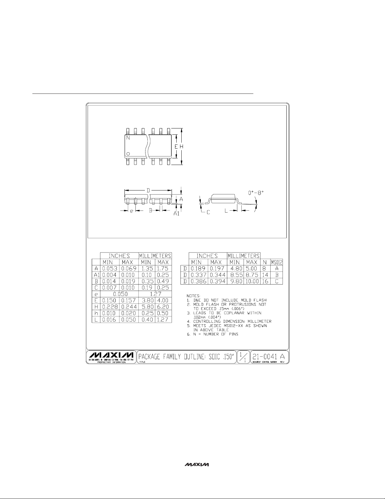
Minimize the current-sense resistor trace length
(<10mm), and ensure accurate current sensing with
Kelvin connections (Figure 12).
When the output is short circuited, the voltage drop
across the external MOSFET becomes large. Hence,
the power dissipation across the switch increases, as
does the die temperature. An efficient way to achieve
good power dissipation on a surface-mount package is
to lay out two copper pads directly under the package
on both sides of the board. Connect the two pads to
the ground plane through vias, and use enlarged copper mounting pads on the top side of the board.
Current-Regulating Hot-Swap Controller with
DualSpeed/BiLevel Fault Protection
14 ______________________________________________________________________________________
V
IN
V
IN
ON
BACKPLANE
MAX4370
VSEN
GATE
CTIM
C
BOARD
V
OUT
REMOVABLE CARD
WITH NO HOT-INSERTION
PROTECTION
Figure 11. Using the MAX4370 on the Backplane
Page 15
MAX4370
Current-Regulating Hot-Swap Controller with
DualSpeed/BiLevel Fault Protection
______________________________________________________________________________________ 15
Pin Configuration
Chip Information
TRANSISTOR COUNT: 1792
MAX4370
SENSE RESISTOR
HIGH-CURRENT PATH
Figure 12. Kelvin Connections for the Current-Sense Resistors
CTIM
CSPDGND
1
2
87ON
STATVSEN
GATE
V
IN
SO
TOP VIEW
3
4
6
5
MAX4370
Page 16
MAX4370
Current-Regulating Hot-Swap Controller with
DualSpeed/BiLevel Fault Protection
Maxim cannot assume responsibility for use of any circuitry other than circuitry entirely embodied in a Maxim product. No circuit patent licenses are
implied. Maxim reserves the right to change the circuitry and specifications without notice at any time.
16
____________________Maxim Integrated Products, 120 San Gabriel Drive, Sunnyvale, CA 94086 408-737-7600
© 1999 Maxim Integrated Products Printed USA is a registered trademark of Maxim Integrated Products.
Maxim cannot assume responsibility for use of any circuitry other than circuitry entirely embodied in a Maxim product. No circuit patent licenses are
implied. Maxim reserves the right to change the circuitry and specifications without notice at any time.
16
____________________Maxim Integrated Products, 120 San Gabriel Drive, Sunnyvale, CA 94086 408-737-7600
© 1999 Maxim Integrated Products Printed USA is a registered trademark of Maxim Integrated Products.
Package Information
SOICN.EPS
 Loading...