

Datasheet MAX4372TESA, MAX4372HEUK-T, MAX4372HESA, MAX4372FEUK-T, MAX4372FESA Datasheet (Maxim)
...
For free samples & the latest literature: http://www.maxim-ic.com, or phone 1-800-998-8800.
For small orders, phone 1-800-835-8769.
General Description
The MAX4372 low-cost, precision, high-side currentsense amplifier is available in a tiny, space-saving
SOT23-5 package. Offered in three gain versions (T =
+20V/V, F = +50V/V, and H = +100V/V), this device
operates from a single +2.7V to +28V supply and consumes only 30µA. It features a voltage output that eliminates the need for gain-setting resistors and is ideal for
today’s notebook computers, cell phones, and other
systems where battery/DC current monitoring is critical.
High-side current monitoring is especially useful in battery-powered systems since it does not interfere with
the ground path of the battery charger. The input common-mode range of 0 to +28V is independent of the
supply voltage and ensures that the current-sense
feedback remains viable even when connected to a 2cell battery pack in deep discharge.
The user can set the full-scale current reading by
choosing the device (T, F, or H) with the desired voltage gain and selecting the appropriate external sense
resistor. This capability offers a high level of integration
and flexibility, resulting in a simple and compact current-sense solution. For higher bandwidth applications,
refer to the MAX4173T/F/H data sheet.
Applications
Power-Management Systems
General-System/Board-Level Current Monitoring
Notebook Computers
Portable/Battery-Powered Systems
Smart-Battery Packs/Chargers
Cell Phones
Precision-Current Sources
Features
♦ Low-Cost, Compact Current-Sense Solution
♦ 30µA Supply Current
♦ +2.7V to +28V Operating Supply
♦ 0.18% Full-Scale Accuracy
♦ Low 1.5Ω Output Impedance
♦ Three Gain Versions Available
+20V/V (MAX4372T)
+50V/V (MAX4372F)
+100V/V (MAX4372H)
♦ Wide 0 to +28V Common-Mode Range,
Independent of Supply Voltage
♦ Available in Space-Saving SOT23-5 Package
MAX4372T/F/H
Low-Cost, SOT23, Micropower, High-Side
Current-Sense Amplifier with Voltage Output
________________________________________________________________
Maxim Integrated Products
1
19-1548; Rev 0; 10/99
PART
MAX4372TEUK-T
MAX4372TESA
MAX4372FEUK-T -40°C to +85°C
-40°C to +85°C
-40°C to +85°C
TEMP. RANGE PIN-PACKAGE
5 SOT23-5
8 SO
5 SOT23-5
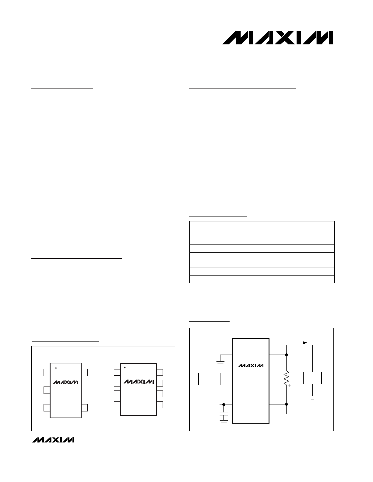
Pin Configurations
Ordering Information
TOP
MARK
ADIU
—
ADIV
MAX4372FESA
MAX4372HEUK-T
MAX4372HESA -40°C to +85°C
-40°C to +85°C
-40°C to +85°C 8 SO
5 SOT23-5
8 SO
—
ADIW
—
RS-
OUT
A/D
CONVERTER
V
CC
V
CC
GND
RS+
R
SENSEVSENSE
I
LOAD
V
IN
0 TO 28V
+2.7V TO +28V
0.1µF
MAX4372T/F/H
LOAD/
BATTERY
Typical Operating Circuit
Note: Gain values are as follows: +20V/V for the T version,
+50V/V for the F version, and +100V/V for the H version.
TOP VIEW
GND
15RS-
MAX4372T/F/H
OUT
2
V
CC
34
SOT23-5
RS+
GND
V
CC
1
2
MAX4372T/F/H
3
4
SO
87RS+
N.C.N.C.
RS-
6
N.C.OUT
5
MAX4372T/F/H
Low-Cost, SOT23, Micropower, High-Side
Current-Sense Amplifier with Voltage Output
2 _______________________________________________________________________________________
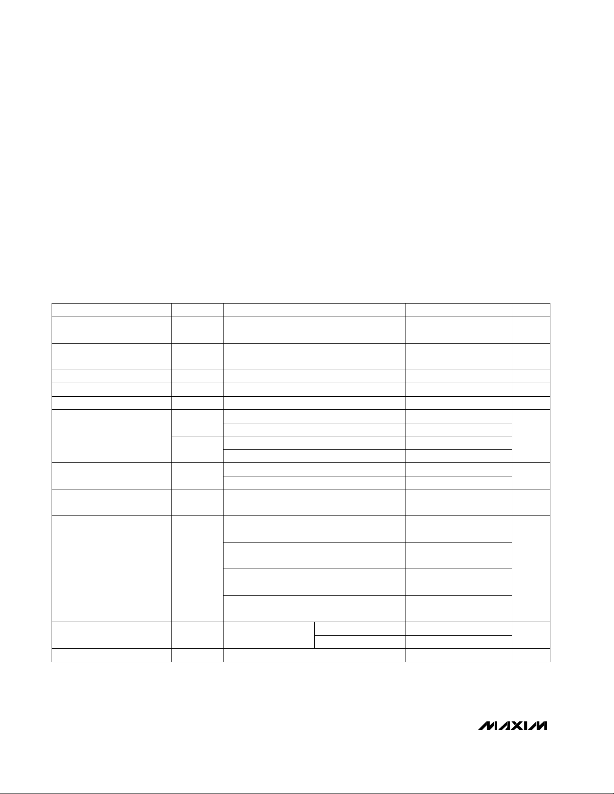
ABSOLUTE MAXIMUM RATINGS
ELECTRICAL CHARACTERISTICS
(V
RS+
= 0 to +28V, VCC= +2.7V to +28V, V
SENSE
= 0, R
LOAD
= 1MΩ, T
A
= T
MIN
to T
MAX
, unless otherwise noted. Typical values are
at T
A
= +25°C.) (Note 1)
Stresses beyond those listed under “Absolute Maximum Ratings” may cause permanent damage to the device. These are stress ratings only, and functional
operation of the device at these or any other conditions beyond those indicated in the operational sections of the specifications is not implied. Exposure to
absolute maximum rating conditions for extended periods may affect device reliability.
VCC, RS+, RS- to GND ...........................................-0.3V to +30V
OUT to GND ...........................................................-0.3V to +15V
Differential Input Voltage (V
RS+
- V
RS-
) ..............................±0.3V
Current into Any Pin..........................................................±10mA
Continuous Power Dissipation (T
A
= +70°C)
5-Pin SOT23 (derate 7.1mW/°C above +70°C).............571mW
8-Pin SO (derate 5.88mW/°C above +70°C).................471mW
Operating Temperature Range ...........................-40°C to +85°C
Storage Temperature Range .............................-65°C to +150°C
Lead Temperature (soldering, 10sec). ............................+300°C
VCC= 2.7V, I
OUT
= -500µA
VCC= 2.7V
V
RS+
≤ 2V
V
RS+
> 2V
V
RS+
≤ 2V
V
RS+
> 2V
V
RS+
> 2V
V
RS+
> 2V, V
SENSE
= 5mV
Gain = +100V/V
VCC= 0
Gain = +20V/V or +50V/V
CONDITIONS
V0.1 0.25VCC- V
OH
OUT High Voltage
965
OUT Low Voltage mV
2.6
mV
100
V
SENSE
150
Full-Scale Sense Voltage
(Note 4)
V028V
CMR
Common-Mode Input Range
(Note 3)
V2.7 28V
CC
Operating Voltage Range
(Note 2)
µA
-50 2
I
RS-
Input Bias Current
02
-25 2
I
RS+
01
dB85CMRCommon-Mode Rejection
µA30 60I
CC
Supply Current
µA0.05 1.2I
RS+
, I
RS-
Leakage Current
UNITSMIN TYP MAXSYMBOLPARAMETER
I
OUT
= 10µA
I
OUT
= 100µA
V
SENSE
= 100mV, VCC= 12V,
V
RS+
= 12V, TA= +25°C (Note 6)
%±0.18 ±3
Full-Scale Accuracy
(Note 5)
V
SENSE
= 100mV, VCC= 12V,
V
RS+
= 12V (Note 6)
±6
V
SENSE
= 100mV, VCC= 28V,
V
RS+
= 28V (Note 6)
±0.15 ±7
V
SENSE
= 100mV, VCC= 12V,
V
RS+
= 0.1V (Note 6)
±1 ±28
V
SENSE
= 6.25mV, VCC= 12V,
V
RS+
= 12V (Note 7)
%
±0.15
Total OUT Voltage Error
(Note 5)
MAX4372T/F/H
Low-Cost, SOT23, Micropower, High-Side
Current-Sense Amplifier with Voltage Output
_______________________________________________________________________________________ 3
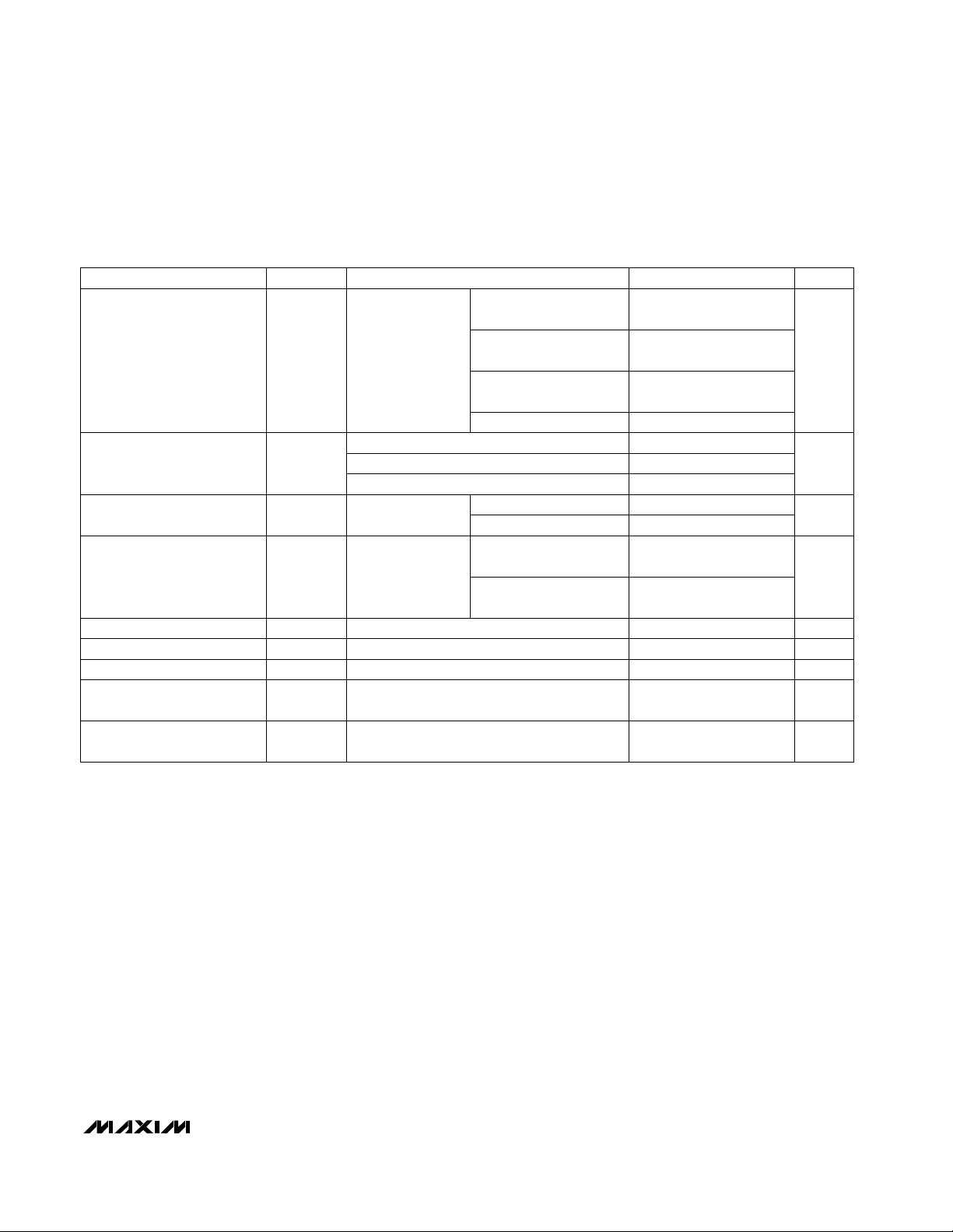
ELECTRICAL CHARACTERISTICS (continued)
(V
RS+
= 0 to +28V, VCC= +2.7V to +28V, V
SENSE
= 0, R
LOAD
= 1MΩ, T
A
= T
MIN
to T
MAX
, unless otherwise noted. Typical values are
at T
A
= +25°C.) (Note 1)
Note 1: All devices are 100% production tested at T
A
= +25°C. All temperature limits are guaranteed by design.
Note 2: Guaranteed by PSR test.
Note 3: Guaranteed by OUT Voltage Error test.
Note 4: Output voltage is internally clamped not to exceed 12V.
Note 5: Total OUT voltage error is the sum of gain and offset voltage errors.
Note 6: Measured at I
OUT
= -500µA (R
LOAD
= 4kΩ for gain = +20V/V, R
LOAD
= 10kΩ for gain = +50V/V, R
LOAD
= 20kΩ for gain =
+100V/V).
Note 7: +6.25mV = 1/16 of +100mV full-scale voltage (C/16).
Note 8: The device will not reverse phase when overdriven.
V
RS
+
= 12V,
V
CC
= 12V,
C
LOAD
= 10pF
CONDITIONS
MAX4372T 20
V
SENS
E
= 100mV,
gain = +20V/V
kHz
50
BW
275
UNITSMIN TYP MAXSYMBOLPARAMETER
V
SENSE
= 100mV,
gain = +50V/V
200
V
SENSE
= 100mV,
gain = +100V/V
110
-3dB Bandwidth
MAX4372F
MAX4372H
V/V
100
Gain 50
No sustained oscillations
V
SENSE
= 100mV Ω1.5R
OUT
OUT Output Resistance
pF1000Capacitive Load Stability
V
SENSE
= 20mV
to 100mV
%
±5.5
Gain Accuracy
V
OUT
= 2V, V
RS+
> 2V
VCC= 12V, V
RS+
= 12V, C
LOAD
= 10pF ms0.1
Saturation Recovery Time
(Note 8)
VCC= 12V, V
RS+
= 12V,
V
SENSE
= 100mV, C
LOAD
= 10pF
ms0.5
Power-Up Time to 1% of
Final Value
dB75 85PSRPower-Supply Rejection
V
SENSE
= 6.25mV
±0.25 ±2.5TA= +25°C
TA= -40°C to +85°C
V
SENSE
= 6.25mV to
100mV
20
V
SENSE
= 100mV to
6.25mV
Gain = +20V/V,
VCC= 12V,
V
RS+
= 12V,
C
LOAD
= 10pF
µs
20
OUT Settling Time to 1% of
Final Value

MAX4372T/F/H
Low-Cost, SOT23, Micropower, High-Side
Current-Sense Amplifier with Voltage Output
4 _______________________________________________________________________________________
Typical Operating Characteristics
(VCC= +12V, V
RS+
= 12V, V
SENSE
= 100mV, TA = +25°C, unless otherwise noted.)
25.0
27.5
30.0
32.5
35.0
SUPPLY CURRENT vs. SUPPLY VOLTAGE
MAX4372 toc01
SUPPLY VOLTAGE (V)
SUPPLY CURRENT (µA)
012164 8 20 24 28
AV = +100V/V
AV = +50V/V
AV = +20V/V
V
SENSE
= 5mV
0
5
10
15
20
25
30
35
40
-40 10 60-15 35 85
SUPPLY CURRENT vs. TEMPERATURE
MAX4372T toc02
TEMPERATURE (°C)
SUPPLY CURRENT (µA)
V
SENSE
= 5mV
28.0
29.0
28.5
30.0
29.5
31.5
31.0
30.5
32.0
SUPPLY CURRENT
vs. COMMON-MODE VOLTAGE
MAX4372 toc03
COMMON-MODE VOLTAGE (V)
SUPPLY CURRENT (µA)
012164 8 20 24 28
AV = +100V/V
AV = +50V/V
AV = +20V/V
V
SENSE
= 5mV
-1.2
-0.8
-1.0
-0.2
-0.4
-0.6
0.4
0.2
0
0.6
0105 15202530
TOTAL OUTPUT ERROR
vs. SUPPLY VOLTAGE
MAX4372 toc04
SUPPLY VOLTAGE (V)
OUTPUT ERROR (%)
G = +100V/V
G = +50V/V
G = +20V/V
0
0.2
0.4
0.6
0.8
1.0
1.2
1.4
1.6
0105 15202530
TOTAL OUTPUT ERROR
vs. COMMON-MODE VOLTAGE
MAX4372T toc07
COMMON-MODE VOLTAGE (V)
OUTPUT ERROR (%)
G = +100V/V
G = +50V/V
G = +20V/V
-1.0
-0.5
0.5
0
1.0
1.5
0 10050 150 200 250 300
TOTAL OUTPUT ERROR vs. V
SENSE
MAX4372T toc05
V
SENSE
(mV)
OUTPUT ERROR (%)
AV = +100V/V
AV = +20V/V
AV = +50V/V
-45
-90
100 100k10k1k
POWER-SUPPLY REJECTION
vs. FREQUENCY
-75
-85
-55
-65
-40
-70
-80
-50
-60
MAX4372T toc06
FREQUENCY (Hz)
PSR (dB)
-1.0
-0.9
-0.8
-0.7
-0.6
-0.5
-0.4
-0.3
-0.2
-0.1
0
GAIN ACCURACY vs. TEMPERATURE
MAX4372T toc08
TEMPERATURE (°C)
GAIN ACCURACY (%)
-40 10 60-15 35 85
AV = +20V/V
AV = +50V/V
AV = +100V/V
-1.0
-0.8
-0.6
-0.4
-0.2
0
0.2
0.4
0.6
0.8
1.0
-40 10 60-15 35 85
TOTAL OUTPUT ERROR vs. TEMPERATURE
MAX4372T toc09
TEMPERATURE (°C)
TOTAL OUTPUT ERROR (%)
AV = +50V/V
AV = +100V/V
AV = +20V/V

V
OUT
V
SENSE
600mV
200mV
30mV
10mV
MAX4372T
SMALL-SIGNAL TRANSIENT RESPONSE
MAX4372T toc10
20µs/div
V
OUT
V
SENSE
1.5V
0.5V
30mV
10mV
MAX4372F
SMALL-SIGNAL TRANSIENT RESPONSE
MAX4372T toc11
20µs/div
V
OUT
V
SENSE
3V
1V
30mV
10mV
MAX4372H
SMALL-SIGNAL TRANSIENT RESPONSE
MAX4372T toc12
20µs/div
V
OUT
V
SENSE
1V
3V
50mV
150mV
MAX4372T
LARGE-SIGNAL TRANSIENT RESPONSE
MAX4372T toc13
20µs/div
V
OUT
V
SENSE
2.5V
7.5V
50mV
150mV
MAX4372F
LARGE-SIGNAL TRANSIENT RESPONSE
20µs/div
MAX4372T toc14
3
-8
1k 100k10k 1M
SMALL-SIGNAL GAIN vs. FREQUENCY
-7
MAX4372T toc16
FREQUENCY (Hz)
GAIN (dB)
-6
-5
-4
-3
-2
-1
0
1
2
G = +50V/V
G = +20V/V
G = +100V/V
V
OUT
V
SENSE
0
10V
0
100mV
MAX4372H
LARGE-SIGNAL TRANSIENT RESPONSE
20µs/div
MAX4372T toc15
MAX4372T/F/H
Low-Cost, SOT23, Micropower, High-Side
Current-Sense Amplifier with Voltage Output
_______________________________________________________________________________________
5
Typical Operating Characteristics (continued)
(VCC= +12V, V
RS+
= 12V, V
SENSE
= 100mV, TA = +25°C, unless otherwise noted.)

_______________Detailed Description
The MAX4372 high-side current-sense amplifier features a 0 to +28V input common-mode range that is
independent of supply voltage. This feature allows the
monitoring of current flow out of a battery in deep discharge, and also enables high-side current sensing at
voltages far in excess of the supply voltage (VCC).
Current flows through the sense resistor, generating a
sense voltage (Figure 1). Since A1’s inverting input is
high impedance, the voltage on the negative terminal
equals VIN- V
SENSE
. A1 forces its positive terminal to
match its negative terminal; therefore, the voltage
across RG1(VIN- V1-) equals V
SENSE
. This creates a
current to flow through RG1equal to V
SENSE
/ RG1. The
transistor and current mirror amplify the current by a
factor of β. This makes the current flowing out of the
current mirror equal to:
I
M
= β V
SENSE
/ R
G1
A2’s positive terminal presents high impedance, so this
current flows through RGD, with the following result:
V2+= R
GD
β · V
SENSE
/ R
G1
R1 and R2 set the closed-loop gain for A2, which
amplifies V2+, yielding:
V
OUT
= R
GD
· β · V
SENSE
/ RG1(1 + R2 / R1)
The gain of the device equals:
V
OUT
= R
GD
· β (1 + R2 / R1) / R
G1
V
SENSE
__________Applications Information
Recommended Component Values
The MAX4372 operates over a wide variety of current
ranges with different sense resistors. Table 1 lists common resistor values for typical operation of the
MAX4372.
Choosing R
SENSE
Given the gain and maximum load current, select
R
SENSE
such that VCC- V
OUT
does not exceed +0.25V
and V
OUT
does not exceed +10V. To measure lower
currents more accurately, use a high value for R
SENSE
.
A higher value develops a higher sense voltage, which
overcomes offset voltage errors of the internal current
amplifier.
In applications monitoring very high current, ensure
R
SENSE
is able to dissipate its own I2R losses. If the
resistor’s rated power dissipation is exceeded, its value
may drift or it may fail altogether, causing a differential
voltage across the terminals in excess of the absolute
maximum ratings.
MAX4372T/F/H
Low-Cost, SOT23, Micropower, High-Side
Current-Sense Amplifier with Voltage Output
6 _______________________________________________________________________________________
Pin Description
1 3 Ground
2 4 Output Voltage. V
OUT
is proportional to the magnitude of V
SENSE(VRS+
- V
RS-
).
PIN
GND
OUT
SO
FUNCTION
SOT23-5
NAME
3 1 Supply Voltage
4 8 Power Connection to the External Sense Resistor
V
CC
RS+
5 6 Load-Side Connection to the External Sense Resistor
— 2, 5, 7 No Connection. Not internally connected.
RS-
N.C.
Figure 1. Functional Diagram
+2.7V
V
CC
TO
+28V
CURRENT
MIRROR
MAX4372T/F/H
OUT
RS+
RS-
GND
R
SENSE
0 TO +28V
I
LOAD
LOAD
V
IN
V
SENSE
TO
R
G1
V1+
A1
V1-
R
G2
R
I
M
A2
R2
GD
V2+
V2-
R1

MAX4372T/F/H
Low-Cost, SOT23, Micropower, High-Side
Current-Sense Amplifier with Voltage Output
_______________________________________________________________________________________ 7
Using a PC Board Trace as R
SENSE
If the cost of R
SENSE
is an issue and accuracy is not
critical, use the alternative solution shown in Figure 2.
This solution uses copper PC board traces to create a
sense resistor. The resistivity of a 0.1-inch-wide trace of
2-ounce copper is about 30mΩ/ft. The resistance tem-
perature coefficient of copper is fairly high (approximately 0.4%/°C), so systems that experience a wide
temperature variance must compensate for this effect.
In addition, self-heating will introduce a nonlinearity
error. Do not exceed the maximum power dissipation of
the copper trace.
For example, the MAX4372T (with a maximum load current of 10A and an R
SENSE
of 5mΩ) creates a full-scale
V
SENSE
of 50mV that yields a maximum V
OUT
of 1V.
R
SENSE
, in this case, requires about 2 inches of 0.1-
inch-wide copper trace.
Table 1. Recommended Component Values
FULL-SCALE LOAD
CURRENT,
I
LOAD
(A)
GAIN
(V/V)
CURRENT-SENSE
RESISTOR,
R
SENSE
(mΩ)
2.0
FULL-SCALE OUTPUT
VOLTAGE (FULL-SCALE
V
SENSE
= 100mV),
V
OUT
(V)
5.0
10.0
0.1 1000
20
100
50
2.0
100
50 5.0
10.0
1 100
20
2.0
100
50 5.0
2.0
100
50 5.0
10.0
5 20
20
10.0
10 10
20
Figure 2. Connections Showing Use of PC Board
Chip Information
TRANSISTOR COUNT: 225
INPUT LOAD/BATTERY
0.1in COPPER 0.3in COPPER0.3in COPPER
RS+
MAX4372T/F/H
RS-
R
V
SENSE
SENSE
V
OUT
GND
CC
+2.7V TO +28V

MAX4372T/F/H
Low-Cost, SOT23, Micropower, High-Side
Current-Sense Amplifier with Voltage Output
Maxim cannot assume responsibility for use of any circuitry other than circuitry entirely embodied in a Maxim product. No circuit patent licenses are
implied. Maxim reserves the right to change the circuitry and specifications without notice at any time.
8
_____________________Maxim Integrated Products, 120 San Gabriel Drive, Sunnyvale, CA 94086 408-737-7600
© 1999 Maxim Integrated Products Printed USA is a registered trademark of Maxim Integrated Products.
Package Information
SOT5L.EPS
 Loading...