

General Description
The MAX4330–MAX4334 single/dual/quad op amps
combine a wide 3MHz bandwidth, low-power operation,
and excellent DC accuracy with Rail-to-Railinputs and
outputs. These devices require only 245µA per amplifier,
and operate from either a single +2.3V to +6.5V supply
or dual ±1.15V to ±3.25V supplies. The input commonmode voltage range extends 250mV beyond VEEand
VCC, and the outputs swing rail-to-rail. The MAX4331/
MAX4333 feature a shutdown mode in which the output
goes high impedance and the supply current decreases
to 9µA per amplifier.
Low-power operation combined with rail-to-rail input
common-mode range and output swing makes these
amplifiers ideal for portable/battery-powered equipment
and other low-voltage, single-supply applications.
Although the minimum operating voltage is specified at
2.3V, these devices typically operate down to 2.0V. Low
offset voltage and high speed make these amplifiers
excellent choices for signal-conditioning stages in precision, low-voltage data-acquisition systems. The
MAX4330 is available in the space-saving 5-pin SOT23
package, and the MAX4331/MAX4333 are offered in
a µMAX package.
Applications
Portable/Battery-Powered Equipment
Data-Acquisition Systems
Signal Conditioning
Low-Power, Low-Voltage Applications
____________________________Features
♦ 3MHz Gain-Bandwidth Product
♦ 245µA Quiescent Current per Amplifier
♦ Available in Space-Saving SOT23-5 Package
(MAX4330)
♦ +2.3V to +6.5V Single-Supply Operation
♦ Rail-to-Rail Input Common-Mode Voltage Range
♦ Rail-to-Rail Output Voltage Swing
♦ 250µV Offset Voltage
♦ Low-Power, 9µA (per amp) Shutdown Mode
(MAX4331/MAX4333)
♦ No Phase Reversal for Overdriven Inputs
♦ Capable of Driving 2kΩ Loads
♦ Unity-Gain Stable
MAX4330–MAX4334
Single/Dual/Quad, Low-Power, Single-Supply,
Rail-to-Rail I/O Op Amps with Shutdown
________________________________________________________________
Maxim Integrated Products
1
V
EE
IN-
IN+
1
5
V
CC
OUT
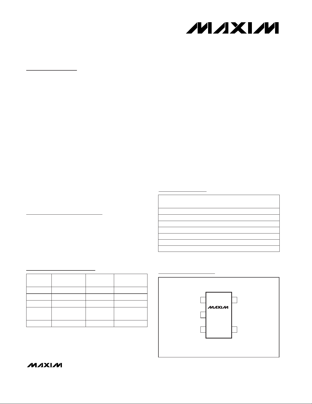
MAX4330
SOT23-5
TOP VIEW
2
3
4
Pin Configurations
19-1192; Rev 3; 2/98
PART
MAX4330EUK-T
MAX4331ESA
-40°C to +85°C
-40°C to +85°C
TEMP. RANGE
PIN-
PACKAGE
5 SOT23-5
8 SO
Ordering Information
PART
NO. OF AMPS
PER PACKAGE
Selector Guide
MAX4330 1 —
SHUTDOWN
MODE
5-pin SOT23
PIN-PACKAGE
MAX4331 1 8-pin SO/µMAXYes
MAX4332 2 8-pin SO—
MAX4333 2
10-pin µMAX,
14-pin SO
Yes
MAX4334 4 14-pin SO—
MAX4331EUA -40°C to +85°C 8 µMAX
SOT
TOP MARK
ABAJ
—
—
Pin Configurations continued at end of data sheet.
Rail-to-Rail is a registered trademark of Nippon Motorola Ltd.
MAX4332ESA
-40°C to +85°C 8 SO —
MAX4333ESD
-40°C to +85°C 14 SO —
MAX4333EUB -40°C to +85°C 10 µMAX —
MAX4334ESD
-40°C to +85°C 14 SO —
For free samples & the latest literature: http://www.maxim-ic.com, or phone 1-800-998-8800.
For small orders, phone 408-737-7600 ext. 3468.
MAX4330–MAX4334
Single/Dual/Quad, Low-Power, Single-Supply,
Rail-to-Rail I/O Op Amps with Shutdown
2 _______________________________________________________________________________________
ABSOLUTE MAXIMUM RATINGS
DC ELECTRICAL CHARACTERISTICS
(VCC= +2.3V to +6.5V, VEE= 0V, VCM= 0V, V
OUT
= (VCC/ 2), RLtied to (VCC/ 2), V
SHDN
≥ 2V, TA= +25°C, unless otherwise noted.)
Stresses beyond those listed under “Absolute Maximum Ratings” may cause permanent damage to the device. These are stress ratings only, and functional
operation of the device at these or any other conditions beyond those indicated in the operational sections of the specifications is not implied. Exposure to
absolute maximum rating conditions for extended periods may affect device reliability.
Supply Voltage, VCCto VEE.....................................................7V
IN_+, IN_-, SHDN Voltage................(V
EE
- 0.3V) to (VCC+ 0.3V)
Output Short-Circuit Duration.................................... Continuous
(short to either supply)
Continuous Power Dissipation (T
A
= +70°C)
5-Pin SOT23 (derate 7.1mW/°C above +70°C).............571mW
8-Pin SO (derate 5.88mW/°C above +70°C).................471mW
8-Pin µMAX (derate 4.10mW/°C above +70°C)............330mW
10-Pin µMAX (derate 5.60mW/°C above +70°C)..........444mW
14-Pin SO (derate 8.33mW/°C above +70°C)...............667mW
Operating Temperature Ranges
MAX433_C/D .......................................................0°C to +70°C
MAX433_E_ _....................................................-40°C to +85°C
Maximum Junction Temperature .....................................+150°C
Storage Temperature Range.............................-65°C to +160°C
Lead Temperature (soldering, 10sec).............................+300°C
| V
IN
+ - VIN- | > 2.5V
| V
IN
+ - VIN- | < 1.4V
VEE< VCM< V
CC
CONDITIONS
kΩ2
R
IN(DIFF)
Differential Input Resistance
MΩ2.3
nA±1 ±12I
OS
Input Offset Current
mV
±0.25 ±0.9
±0.65 ±1.5
UNITSMIN TYP MAXSYMBOLPARAMETER
71 93
74 93
67 87
68 88
V
-0.25 VCC+
0.25
V
CM
Common-Mode Input
Voltage Range
V
SHDN
< 0.8V, V
OUT
= 0V to V
CC
µA±0.1 ±2I
OUT(SHDN)
Off-Leakage Current
in Shutdown
dB
69 92
CMRR
Common-Mode
Rejection Ratio
±0.65 ±1.5
±0.25 ±0.6V
OS
Input Offset Voltage
MAX433_EUA/EUB
MAX4330EUK
MAX4331ESA
MAX4332ESA/
MAX4333ESD
MAX4334ESD
-0.25V <
VCM<
(VCC+ 0.25V)
VCC=
5V
VCM=
VEEto V
CC
MAX433_EUA/EUB
MAX4331ESA
MAX4330EUK
VEE< VCM< V
CC
±25 ±65I
B
Input Bias Current
MAX4332ESA/MAX4333ESD
MAX433_EUA/EUB
69 90
71 90
64 82
65 84
MAX4330EUK
MAX4331ESA
MAX4332ESA/
MAX4333ESD
dB
66 89MAX4334ESD
MAX433_EUA/EUB
VCC= 2.3V to 6.5VPSSRPower-Supply Rejection Ratio
77 90
79 92
76 88
76 88
MAX4330EUK
MAX4331ESA
MAX4332ESA/
MAX4333ESD
dB
75 90MAX4334ESD
VCC=
2.3V
±0.25 ±1.0MAX4334ESD
nA
AV= 1 Ω0.1R
OUT
Output Resistance
mA
MAX4330–MAX4334
Single/Dual/Quad, Low-Power, Single-Supply,
Rail-to-Rail I/O Op Amps with Shutdown
_______________________________________________________________________________________ 3
DC ELECTRICAL CHARACTERISTICS (continued)
(VCC= +2.3V to +6.5V, VEE= 0V, VCM= 0V, V
OUT
= (VCC/ 2), RLtied to (VCC/ 2), V
S HDN
≥ 2V, TA= +25°C, unless otherwise noted.)
Low (shutdown mode)
CONDITIONS
0.8
V
SHDN
< 0.8V
VEE< V
SHDN
< V
CC
High (normal mode)
VCM= V
OUT
= VCC/ 2
µA
9 14
V2.3 6.5V
CC
Operating Supply-Voltage
Range
µA±2
SHDN Input Current
V
2.0
V
IL
SHDN Logic Threshold
(Note 1)
I
CC(SHDN)
Shutdown Supply Current
per Amplifier
17 25
µA
245 290
I
CC
Quiescent Supply Current
per Amplifier
275 325
UNITSMIN TYP MAXSYMBOLPARAMETER
VCC= 5V
VCC= 2.3V
VCC= 5V
VCC= 2.3V
VEE< VCM< V
CC
VCC= 2.3V to 6.5V
MAX433_EUA
73
76
71
72
CONDITIONS
nA±15I
OS
Input Offset Current
MAX433_EUK/EUB
MAX4331ESA
dB
71
PSRRPower-Supply Rejection Ratio
MAX4332ESA/
MAX4333ESD
MAX4334ESD
±1
±3.2
UNITSMIN TYP MAXSYMBOLPARAMETER
±3.8
VCM=
VEEto V
CC
mV
±0.7
V
OS
Input Offset Voltage
VEE< VCM< V
CC
nA±115I
B
Input Bias Current
V
IH
mV
70 150
mA20I
SC
Output Short-Circuit Current
RL = 2kΩ
100 175
8 30
RL = 100kΩ
8 30
V
OUT
Output Voltage Swing
dB
83 95
VCC= 5V
93 120
78 90
93 112
A
VOL
Large-Signal Voltage Gain
V
OUT
= 0.2V to 2.1V, RL= 100kΩ
VCC= 2.3V
V
OUT
= 0.35V to 1.95V, RL= 2kΩ
V
OUT
= 0.2V to 4.8V, RL= 100kΩ
V
OUT
= 0.35V to 4.65V, RL= 2kΩ
VCC- V
OH
V
OL
VCC- V
OH
V
OL
±1
DC ELECTRICAL CHARACTERISTICS
(VCC= +2.3V to +6.5V, VEE= 0V, VCM= 0V, V
OUT
= (VCC/ 2), RLtied to (VCC/ 2), V
SHDN
≥ 2V, TA= -40°C to +85°C, unless
otherwise noted.)
MAX433_EUA
MAX4332ESA/MAX4333ESD
MAX4331ESA
MAX433_EUK/EUB
µV/°C±3∆VOS/∆TOffset-Voltage Tempco
MAX4334ESD
-0.15 VCC+
0.15
V
CM
Common-Mode Input
Voltage Range
V
MAX4330–MAX4334
Single/Dual/Quad, Low-Power, Single-Supply,
Rail-to-Rail I/O Op Amps with Shutdown
4 _______________________________________________________________________________________
DC ELECTRICAL CHARACTERISTICS (continued)
(VCC= +2.3V to +6.5V, VEE= 0V, VCM= 0V, V
OUT
= (VCC/ 2), RLtied to (VCC/ 2), V
SHDN
≥ 2V, TA= -40°C to +85°C, unless
otherwise noted.)
VCC= 2.3V
VCC= 5V
Low (shutdown mode)
VCC= 5V
VCC= 2.3V
CONDITIONS
0.8
V
SHDN
< 0.8V
VEE< V
SHDN
< V
CC
High (normal mode)
VCM= V
OUT
= VCC/ 2
µA
17
V2.3 6.5V
CC
Operating Supply-Voltage
Range
µA±2
SHDN Input Current
V
2.0
V
IL
SHDN Logic Threshold
(Note 1)
I
CC(SHDN)
Shutdown Supply Current
per Amplifier
30
µA
330
I
CC
Quiescent Supply Current
per Amplifier
350
UNITSMIN TYP MAXSYMBOLPARAMETER
TA= -40°C to +85°C
Note 1: SHDN logic thresholds are referenced to VEE.
Note 2: The MAX4330EUK is 100% tested at T
A
= +25°C. All temperature limits are guaranteed by design.
V
IH
RL= 2kΩ
200V
CC - VOH
180V
OL
40V
OL
RL= 100kΩ
40
mVV
OUT
Output Voltage Swing
V
CC - VOH
74V
OUT
= 0.35V to 4.65V, RL = 2kΩ
VCC= 5V
90V
OUT
= 0.2V to 4.8V, RL = 100kΩ
70V
OUT
= 0.35V to 1.95V, RL = 2kΩ
VCC= 2.3V
90
dBA
VOL
Large-Signal Voltage Gain
V
OUT
= 0.2V to 2.1V, RL = 100kΩ
±5 µAI
OUT(SHDN)
Off-Leakage Current
in Shutdown
V
SHDN
< 0.8V, V
OUT
= 0V to V
CC
63
CMRR dB
Common-Mode
Rejection Ratio
MAX433_EUA/EUB
VCC=
5V
62MAX4330EUK
72MAX4331ESA
69
MAX4332ESA/
MAX4333ESD
67MAX4334ESD
58MAX433_EUA/EUB
VCC=
2.3V
57MAX4330EUK
68MAX4331ESA
66
MAX4332ESA/
MAX4333ESD
65MAX4334ESD
-0.25V <
VCM<
(V
CC
+ 0.25V)
MAX4330–MAX4334
Single/Dual/Quad, Low-Power, Single-Supply,
Rail-to-Rail I/O Op Amps with Shutdown
_______________________________________________________________________________________ 5
AC ELECTRICAL CHARACTERISTICS
(VCC= +5V, VEE= 0V, VCM= 0V, V
OUT
= (VCC/ 2), RL = 10kΩ to (VCC/ 2), V
SHDN
≥ 2V, CL= 15pF, TA= +25°C, unless
otherwise noted.)
Slew Rate SR V/µs
Gain Margin GM dB
degrees
10
PMPhase Margin 55
Settling Time to 0.01% t
S
CONDITIONS
AV= +1V/V, 2V step µs
pFC
IN
Input Capacitance 3
f = 10kHz, V
OUT
= 2Vp-p, A
VCL
= +1V/V %
4
THDTotal Harmonic Distortion
Crosstalk
0.012
Capacitive Load Stability
V
OUT
= 4Vp-p
f = 10kHz, MAX4332/MAX4333/MAX4334
f = 10kHz
MHz3GBWPGain-Bandwidth Product
nV/√Hz
V
NOISE
Input Noise Voltage Density 28
dB
f = 10kHz
pA/√Hz
-124
I
NOISE
Input Current Noise Density 0.26
AV= 1, no sustained oscillations pF150
kHz
1.5
Shutdown Time
Enable Time from Shutdown
t
SHDN
µs0.8
t
ENABLE
FPBWFull-Power Bandwidth
µs1
190
Power-Up Time t
ON
µs5
UNITSMIN TYP MAXSYMBOLPARAMETER
60
-20
100 1k 100k 10M
GAIN AND PHASE
vs. FREQUENCY (NO LOAD)
MAX4330/34-TOC01
FREQUENCY (Hz)
GAIN (dB)
PHASE (DEGREES)
10k 1M 100M
50
40
30
20
10
0
-10
180
-180
135
90
45
0
-45
-90
-135
GAIN
PHASE
AV = +1000
60
-40
100 1k 100k 10M
GAIN AND PHASE
vs. FREQUENCY (C
L
= 150pF)
MAX4330/34-TOC02
FREQUENCY (Hz)
GAIN (dB)
PHASE (DEGREES)
10k 1M 100M
40
20
0
-20
180
-180
108
36
-36
-108
144
72
0
-72
-144
GAIN
AV = +1000
PHASE
0
-100
10 100
10k
1M 10M
POWER-SUPPLY REJECTION RATIO
vs. FREQUENCY
MAX4330/34-TOC03
FREQUENCY (Hz)
PSRR (dB)
1k
100k
100M
-20
-40
-60
-80
AV = +1
__________________________________________Typical Operating Characteristics
(VCC= +5V, VEE= 0V, VCM= VCC/ 2, V
SHDN
> 2V, TA= +25°C, unless otherwise noted.)

MAX4330–MAX4334
Single/Dual/Quad, Low-Power, Single-Supply,
Rail-to-Rail I/O Op Amps with Shutdown
6 _______________________________________________________________________________________
-40
-20
-30
10
0
-10
40
30
20
50
-40 0 20-20 40 60 80 100
INPUT BIAS CURRENT
vs. TEMPERATURE
MAX4330-34 TOC8a
TEMPERATURE (°C)
INPUT BIAS CURRENT (nA)
V
CC
= 6.5V, V
CM
= V
CC
V
CC
= 2.7V, V
CM
= V
CC
V
CC
= 6.5V, V
CM
= V
EE
V
CC
= 2.3V, V
CM
= V
EE
250
200
150
100
50
0
MAX4330/34-TOC09
TEMPERATURE (°C)
-20-40-60 200 60 8040 100
OUTPUT SWING HIGH
vs. TEMPERATURE
V
CC
- V
OUT
(mV)
RL TO V
EE
V
CC
= 6.5V, RL = 2kΩ
V
CC
= 2.3V, RL = 2kΩ
V
CC
= 2.3V, RL = 100kΩ
V
CC
= 6.5V, RL = 100kΩ
120
100
80
40
20
60
0
MAX4330/34-TOC12
TEMPERATURE (°C)
-20 0-60 -40 20 40 60 80 100
OUTPUT SWING LOW
vs. TEMPERATURE
V
OUT
- V
EE
(mV)
RL TO V
CC
V
CC
= 2.3V
R
L
= 100kΩ
V
CC
= 6.5V
R
L
= 100kΩ
V
CC
= 2.3V
R
L
= 2kΩ
V
CC
= 6.5V
R
L
= 2kΩ
1k
0.01
100 1k 100k 10M
OUTPUT IMPEDANCE
vs. FREQUENCY
MAX4330/34-TOC04
FREQUENCY (Hz)
OUTPUT IMPEDANCE (Ω)
10k 1M 100M
100
10
1
0.1
AV = +1
1200
1000
800
400
0
200
600
-200
TEMPERATURE (°C)
-40 -20 0-60 20 40 60 80 100
OUTPUT LEAKAGE CURRENT
vs. TEMPERATURE
OUTPUT LEAKAGE CURRENT (pA)
AV = OPEN LOOP
SHDN = 0V
OUT SHORT
TO V
EE
V
CC
= 6.5V
V
CC
= 2.3V
OUT SHORT
TO V
CC
V
CC
= 2.3V TO 6.5V
MAX4330/34-TOC07
350
310
330
250
270
290
210
190
170
230
150
TEMPERATURE (°C)
-20-60 20 60 1000-40 40 80
SUPPLY CURRENT
vs. TEMPERATURE
I
CC
(µA)
MAX4330/34-TOC05
V
CC
= 6.5V
V
CC
= 2.3V
25
20
15
10
5
TEMPERATURE (°C)
-40-60 -20 40 60 80200 100
SHUTDOWN SUPPLY CURRENT
vs. TEMPERATURE
I
CC
(µA)
MAX4330/34-TOC06
SHDN = 0V
V
CC
= 6.5V
V
CC
= 2.3V
1500
500
0
1000
-500
-1000
-1500
TEMPERATURE (°C)
-40 -20 0-60 20 40 60 80 100
INPUT OFFSET VOLTAGE
vs. TEMPERATURE
INPUT OFFSET VOLTAGE (µV)
MAX4330/34-TOC07a
SOT/µMAX PACKAGES
SO PACKAGE
-30
-10
-20
10
0
30
20
40
0 2 31 4 5 6 7
INPUT BIAS CURRENT
vs. COMMON-MODE VOLTAGE
MAX4330-34/TOC08
COMMON-MODE VOLTAGE (V)
INPUT BIAS CURRENT (nA)
VCC = 2.3V
VCC = 6.5V
____________________________Typical Operating Characteristics (continued)
(VCC= +5V, VEE= 0V, VCM= VCC/ 2, V
SHDN
> 2V, TA= +25°C, unless otherwise noted.)

MAX4330–MAX4334
Single/Dual/Quad, Low-Power, Single-Supply,
Rail-to-Rail I/O Op Amps with Shutdown
_______________________________________________________________________________________
7
____________________________Typical Operating Characteristics (continued)
(VCC= +5V, VEE= 0V, VCM= VCC/ 2, V
SHDN
> 2V, TA= +25°C, unless otherwise noted.)
118
108
113
103
93
83
88
98
78
MAX4330/34-TOC13
OUTPUT VOLTAGE: EITHER SUPPLY (V)
0.10 0.2 0.3 0.50.4 0.6
LARGE-SIGNAL GAIN
vs. OUTPUT VOLTAGE
(V
CC
= 2.3V, RL TO VCC)
GAIN (dB)
RL = 100kΩ
RL = 10kΩ
RL = 2kΩ
-60
-70
-80
-90
-110
-130
-120
-100
-140
MAX4330/34-TOC11
TEMPERATURE (°C)
-20-40-60 0 20 806040 100
COMMON-MODE REJECTION
vs. TEMPERATURE
COMMON-MODE REJECTION (dB)
V
CM
= -0.25V
TO +5.25V
115
105
110
100
95
90
85
MAX4330/34-TOC14
TEMPERATURE (°C)
-40-60 -20 0 60 804020 100
LARGE-SIGNAL GAIN
vs. TEMPERATURE (R
L
= 2kΩ)
GAIN (dB)
RL TO V
CC
RL TO V
EE
RL TO V
EE
V
OUT
(p-p) = V
CC
- 1V
RL TO V
CC
V
CC
= 2.3V
V
CC
= 6.5V
118
114
110
106
98
90
94
102
86
MAX4330/34-TOC10
OUTPUT VOLTAGE: EITHER SUPPLY (V)
0.10 0.2 0.50.40.3 0.6
LARGE-SIGNAL GAIN
vs. OUTPUT VOLTAGE
(V
CC
= 2.3V, RL TO VEE)
GAIN (dB)
RL = 10kΩ
RL = 2kΩ
RL = 100kΩ
130
120
125
115
105
95
100
110
90
MAX4330/34-TOC15
OUTPUT VOLTAGE: EITHER SUPPLY (V)
0.10 0.2 0.3 0.50.4 0.6
LARGE-SIGNAL GAIN
vs. OUTPUT VOLTAGE
(V
CC
= 6.5V, RL TO VEE)
GAIN (dB)
RL = 100kΩ
RL = 10kΩ
RL = 2kΩ
140
130
120
100
90
110
80
MAX4330/34-TOC16
OUTPUT VOLTAGE: EITHER SUPPLY (V)
0 0.1 0.2 0.3 0.4 0.5 0.6
LARGE-SIGNAL GAIN
vs. OUTPUT VOLTAGE
(V
CC
= 6.5V, RL TO VCC)
GAIN (dB)
RL = 100kΩ
RL = 10kΩ
RL = 2kΩ
130
125
120
115
110
MAX4330/34-TOC17
TEMPERATURE (°C)
-40-60 -20 0 60 804020 100
LARGE-SIGNAL GAIN
vs. TEMPERATURE (R
L
= 100kΩ)
GAIN (dB)
V
OUT
(p-p) =
V
CC
- 1V
RL TO V
CC
OR V
EE
V
CC
= 2.3V
RL TO V
CC
V
CC
= 6.5V
RL TO V
EE
V
CC
= 6.5V
2.00
1.95
1.90
1.85
1.80
1.75
1.70
1.65
1.60
MAX4330/34-TOC18
TEMPERATURE (°C)
-40-60 -20 0 60 804020 100
MINIMUM OPERATING VOLTAGE
vs. TEMPERATURE
V
CC
(V)
1
0.001
1 1k 10k 100k
TOTAL HARMONIC DISTORTION
AND NOISE vs. FREQUENCY
0.01
0.1
MAX4330/34-TOC19
FREQUENCY (Hz)
THD + NOISE (%)
10010
AV = +1
2Vp-p SIGNAL
500kHz LOWPASS FILTER
R
L
= 10kΩ TO V
CC
/ 2

MAX4330–MAX4334
Single/Dual/Quad, Low-Power, Single-Supply,
Rail-to-Rail I/O Op Amps with Shutdown
8 _______________________________________________________________________________________
1
0.001
4.0 5.0
TOTAL HARMONIC DISTORTION
AND NOISE vs. PEAK-TO-PEAK
SIGNAL AMPLITUDE
0.01
0.1
MAX4330/34-TOC20
PEAK-TO-PEAK SIGNAL AMPLITUDE (V)
THD + NOISE (%)
4.6 4.84.2 4.4
A
V
= +1
1kHz SINE WAVE
500kHz LOWPASS FILTER
R
L
TO V
CC
/ 2
RL = 2kΩ
RL = 10kΩ
RL = 100kΩ
80
100
90
120
110
130
140
1 10 100 1000 10000
CROSSTALK vs. FREQUENCY
MAX4330/34-TOC22
FREQUENCY (kHz)
CROSSTALK (dB)
10
0
0 200 600 1000
CAPACITIVE LOAD STABILITY
8
MAX4330/34-TOC21
LOAD CAPACITANCE (pF)
LOAD RESISTANCE (kΩ)
400 800
6
4
2
UNSTABLE
REGION
RL TO V
EE
V
OUT
= V
CC
/ 2
LARGE-SIGNAL TRANSIENT RESPONSE
(NONINVERTING)
MAX4330/34-TOC24
TIME (5µs/div)
IN
OUT
VOLTAGE (2V/div)
AV = -1
IN
OUT
SMALL-SIGNAL TRANSIENT RESPONSE
(INVERTING)
MAX4330/34-TOC23
TIME (200ns/div)
VOLTAGE (50mV/div)
LARGE-SIGNAL TRANSIENT RESPONSE
(INVERTING)
MAX4330/34-TOC25
TIME (5µs/div)
IN
OUT
VOLTAGE (2V/div)
AV = +1
IN
OUT
SMALL-SIGNAL TRANSIENT RESPONSE
(NONINVERTING)
MAX4330/34-TOC22
TIME (200ns/div)
VOLTAGE (50mV/div)
____________________________Typical Operating Characteristics (continued)
(VCC= +5V, VEE= 0V, VCM= VCC/ 2, V
SHDN
> 2V, TA= +25°C, unless otherwise noted.)

MAX4330–MAX4334
Single/Dual/Quad, Low-Power, Single-Supply,
Rail-to-Rail I/O Op Amps with Shutdown
_______________________________________________________________________________________ 9
Pin Description
V
EE
42
OUT61
44
——
114
——
MAX4333
Negative Supply. Ground for singlesupply operation.
Output
IN-24
IN+33
——
——
——
——
Inverting Input
Noninverting Input
IN1+,
IN2+
——
OUT1,
OUT2
——
3, 73, 5
1, 91, 7
3, 53, 11
1, 71, 13
Noninverting Inputs to Amplifiers
1 and 2
Outputs for Amplifiers 1 and 2
N.C.1, 5—
V
CC
75
——
108
—5, 7, 8, 10
414
No Connection. Not internally
connected.
Positive Supply
SHDN
8—
IN1-,
IN2-
——
——
2, 82, 6
——
2, 62, 12
Shutdown Input for Amplifier. Drive
low for shutdown mode. Drive
high or connect to VCCfor normal
operation.
Inverting Inputs to Amplifiers
1 and 2
IN3+,
IN4+
——
IN3-,
IN4-
——
——
——
10, 12—
9, 13—
Noninverting Inputs for Amplifiers
3 and 4
Inverting Inputs for Amplifiers
3 and 4
OUT3,
OUT4
——
SHDN1,
SHDN2
——
——
5, 6—
8, 14—
—6, 9
Outputs for Amplifiers 3 and 4
Shutdown for Amplifiers 1 and 2.
Drive low for shutdown mode.
Drive high or connect to VCCfor
normal operation.
NAME
10-Pin
µMAX
14-Pin SO
MAX4332MAX4331MAX4330 MAX4334
FUNCTION
PIN

MAX4330–MAX4334
Single/Dual/Quad, Low-Power, Single-Supply,
Rail-to-Rail I/O Op Amps with Shutdown
10 ______________________________________________________________________________________
_______________Detailed Description
Rail-to-Rail Input Stage
The MAX4330–MAX4334 have rail-to-rail input and output stages that are specifically designed for lowvoltage, single-supply operation. The input stage consists of separate NPN and PNP differential stages,
which operate together to provide a common-mode
range extending to 0.25V beyond both supply rails. The
crossover region, which occurs halfway between V
CC
and VEE, is extended to minimize degradation in CMRR
caused by mismatched input pairs. The input offset voltage is typically 250µV. Low offset voltage, high bandwidth, rail-to-rail common-mode input range, and
rail-to-rail outputs make this family of op amps an excellent choice for precision, low-voltage data-acquisition
systems.
Since the input stage consists of NPN and PNP pairs,
the input bias current changes polarity as the input voltage passes through the crossover region. Match the
effective impedance seen by each input to reduce the
offset error due to input bias currents flowing through
external source impedances (Figures 1a and 1b). The
combination of high source impedance with input
capacitance (amplifier input capacitance plus stray
capacitance) creates a parasitic pole that produces an
underdamped signal response. Reducing input capacitance or placing a small capacitor across the feedback
resistor improves response.
The MAX4330–MAX4334’s inputs are protected from
large differential input voltages by internal 1kΩ series
resistors and back-to-back triple diode stacks across
the inputs (Figure 2). For differential input voltages
(much less than 1.8V), input resistance is typically
2.3MΩ. For differential input voltages greater than 1.8V,
input resistance is around 2kΩ, and the input bias current can be approximated by the following equation:
I
BIAS
= (V
DIFF
- 1.8V) / 2kΩ
In the region where the differential input voltage
approaches 1.8V, input resistance decreases exponentially from 2.3MΩ to 2kΩ as the diode block begins conducting. Inversely, the bias current increases with the
same curve.
R3
R3 = R1 R2
R1 R2
MAX4330
MAX4331
MAX4332
MAX4333
MAX4334
Figure 1a. Reducing Offset Error Due to Bias Current
(Noninverting)
R3
R3 = R1 R2
R1 R2
MAX4330
MAX4331
MAX4332
MAX4333
MAX4334
Figure 1b. Reducing Offset Error Due to Bias Current
(Inverting)

MAX4330–MAX4334
Single/Dual/Quad, Low-Power, Single-Supply,
Rail-to-Rail I/O Op Amps with Shutdown
______________________________________________________________________________________ 11
Rail-to-Rail Output Stage
The MAX4330–MAX4334 output stage can drive up to a
2kΩ load and still typically swing within 125mV of the
rails. Figure 3 shows the output voltage swing of a
MAX4331 configured as a unity-gain buffer. The operating voltage is a single +3V supply, and the input voltage is 3Vp-p. The output swings to within 70mV of V
EE
and 100mV of VCC, even with the maximum load
applied (2kΩ to mid-supply).
Driving a capacitive load can cause instability in many
op amps, especially those with low quiescent current.
The MAX4330–MAX4334 are stable for capacitive loads
up to 150pF. The Capacitive Load Stability graph in the
Typical Operating Characteristics
gives the stable
operating region for capacitive vs. resistive loads.
Figures 4 and 5 show the response of the MAX4331
with an excessive capacitive load, compared with the
response when a series resistor is added between the
output and the capacitive load. The resistor improves
the circuit’s response by isolating the load capacitance
from the op amp’s output (Figure 6).
1k
1k
Figure 2. Input Protection Circuit
Figure 3. Rail-to-Rail Input/Output Voltage Range
IN
1V/div
1V/div
OUT
20µs/div
V
CC
= 3V, RL = 2kΩ TO VCC / 2
Figure 4. Small-Signal Transient Response with Excessive
Capacitive Load
IN
50mV/div
50mV/div
OUT
2µs/div
R
ISO
= 0Ω, AV = +1
C
L
= 510pF
V
CC
= 3V, RL = 100kΩ

MAX4330–MAX4334
Single/Dual/Quad, Low-Power, Single-Supply,
Rail-to-Rail I/O Op Amps with Shutdown
12 ______________________________________________________________________________________
__________Applications Information
Power-Up
The MAX4330–MAX4334 outputs typically settle within
5µs after power-up. Using the test circuit of Figure 7,
Figures 8 and 9 show the output voltage and supply
current on power-up and power-down.
Shutdown Mode
The MAX4331/MAX4333 feature a low-power shutdown
mode. When the shutdown pin (SHDN) is pulled low, the
supply current drops to 9µA per amplifier (typical), the
amplifier is disabled, and the outputs enter a highimpedance state. Pulling SHDN high or leaving it floating enables the amplifier. Figures 10 and 11 show the
MAX4331/MAX4333’s output voltage and supply-current
responses to a shutdown pulse.
Figure 5. Small-Signal Transient Response with Excessive
Capacitive Load and Isolation Resistor
IN
50mV/div
50mV/div
OUT
2µs/div
AV = +1, CL = 510pF
R
ISO
= 39Ω
Figure 6. Capacitive-Load-Driving Circuit
R
ISO
C
L
MAX4330
MAX4331
MAX4332
MAX4333
MAX4334
Figure 7. Power-Up/Shutdown Test Circuit
SHDN
V
OUT
0V TO +2.7V
STEP FOR
SHUTDOWN
TEST
0V TO +2.7V STEP
FOR POWER-UP
TEST, +2.7V STEP
FOR SHUTDOWN-
ENABLE TEST
SUPPLY-CURRENT
MONITORING POINT
V
CC
100Ω2k
10k
2k
MAX4330
MAX4331
MAX4332
MAX4333
MAX4334
Figure 8. Power-Up/Down Output Voltage
V
CC
1V/div
500mV/div
OUT
5µs/div

MAX4330–MAX4334
Single/Dual/Quad, Low-Power, Single-Supply,
Rail-to-Rail I/O Op Amps with Shutdown
______________________________________________________________________________________ 13
Do not three-state SHDN. Due to the output leakage
currents of three-state devices and the small internal
pull-up current for SHDN, three-stating this pin could
result in indeterminate logic levels, and could adversely
affect op-amp operation.
The logic threshold for SHDN is always referred to VEE,
not GND. When using dual supplies, pull SHDN to V
EE
to place the op amp in shutdown mode.
Power Supplies and Layout
The MAX4330–MAX4334 operate from a single +2.3V
to +6.5V power supply, or from dual ±1.15V to ±3.25V
supplies. For single-supply operation, bypass the
power supply with a 0.1µF capacitor to ground (VEE).
For dual supplies, bypass both VCCand VEEwith their
own set of capacitors to ground.
Good layout technique helps optimize performance by
decreasing the amount of stray capacitance at the op
amp’s inputs and outputs. To decrease stray capacitance, minimize trace lengths by placing external components close to the op amp’s pins.
Figure 9. Power-Up/Down Supply Current
V
CC
1V/div
100µA/div
I
CC
5µs/div
Figure 11. Shutdown Enable/Disable Supply Current
SHDN
1V/div
100µA/div
I
CC
5µs/div
Figure 10. Shutdown Output Voltage Enable/Disable
SHDN
1V/div
500mV/div
OUT
5µs/div

MAX4330–MAX4334
Single/Dual/Quad, Low-Power, Single-Supply,
Rail-to-Rail I/O Op Amps with Shutdown
14 ______________________________________________________________________________________
Pin Configurations (continued)
OUT
N.C.V
EE
1
2
8
7
SHDN
V
CC
IN-
IN+
N.C.
SO/µMAX
TOP VIEW
3
4
6
5
MAX4331
IN2-
IN2+V
EE
1
2
87V
CC
OUT2IN1-
IN1+
OUT1
SO
3
4
6
5
MAX4332
1
2
3
4
5
10
9
8
7
6
V
CC
OUT2
IN2IN2+
V
EE
IN1+
IN1-
OUT1
MAX4333
µMAX
SHDN2
SHDN1
14
13
12
11
10
9
8
1
2
3
4
5
6
7
OUT4
IN4IN4+
V
EE
V
CC
IN1+
IN1-
OUT1
MAX4334
IN3+
IN3OUT3OUT2
IN2-
IN2+
SO
14
13
12
11
10
9
8
1
2
3
4
5
6
7
V
CC
OUT2
IN2IN2+V
EE
IN1+
IN1-
OUT1
MAX4333
N.C.
SHDN2
N.C.N.C.
SHDN1
N.C.
SO

MAX4330–MAX4334
Single/Dual/Quad, Low-Power, Single-Supply,
Rail-to-Rail I/O Op Amps with Shutdown
______________________________________________________________________________________ 15
P
D
E
F
W
P
2
P
0
D
1
A
0
B
0
K
0
t
±0.102
±0.102
A
0
B
0
D
D
1
3.200
3.099
1.499
0.991
±0.102
±0.051
±0.102
±0.102
1.753
3.505
1.397
3.988
E
F
K
0
P
+0.102
+0.000
NOTE: DIMENSIONS ARE IN MM.
AND FOLLOW EIA481-1 STANDARD.
+0.305
-0.102
+0.254
+0.000
P
0
3.988 ±0.102
P
0
10 40.005 ±0.203
P
2
2.007 ±0.051
t 0.254 ±0.127
W 8.001
5 SOT23-5
Tape-and-Reel Information
Chip Information
MAX4330/MAX4331
TRANSISTOR COUNT: 199
SUBSTRATE CONNECTED TO V
EE
MAX4332/MAX4333
TRANSISTOR COUNT: 398
SUBSTRATE CONNECTED TO V
EE
MAX4334
TRANSISTOR COUNT: 796
SUBSTRATE CONNECTED TO V
EE

MAX4330–MAX4334
Single/Dual/Quad, Low-Power, Single-Supply,
Rail-to-Rail I/O Op Amps with Shutdown
________________________________________________________Package Information
SOT5L.EPS
8LUMAXD.EPS
Maxim cannot assume responsibility for use of any circuitry other than circuitry entirely embodied in a Maxim product. No circuit patent licenses are
implied. Maxim reserves the right to change the circuitry and specifications without notice at any time.
16
____________________Maxim Integrated Products, 120 San Gabriel Drive, Sunnyvale, CA 94086 408-737-7600
© 1998 Maxim Integrated Products Printed USA is a registered trademark of Maxim Integrated Products.
 Loading...