Maxim MAX1655ESE, MAX1655EEE, MAX1653ESE, MAX1653EEE, MAX1652EEE Datasheet
For free samples & the latest literature: http://www.maxim-ic.com, or phone 1-800-998-8800.
For small orders, phone 408-737-7600 ext. 3468.
General Description
The MAX1652–MAX1655 are high-efficiency, pulsewidth-modulated (PWM), step-down DC-DC controllers
in small QSOP packages. The MAX1653/MAX1655 also
come in 16-pin narrow SO packages that are pincompatible upgrades to the popular MAX797. Improvements include higher duty-cycle operation for better
dropout, lower quiescent supply currents for better
light-load efficiency, and an output voltage down to 1V
(MAX1655).
The MAX1652–MAX1655 achieve up to 96% efficiency
and deliver up to 10A using a unique Idle Mode™ synchronous-rectified PWM control scheme. These devices
automatically switch between PWM operation at heavy
loads and pulse-frequency-modulated (PFM) operation
at light loads to optimize efficiency over the entire output current range. The MAX1653/MAX1655 also feature
logic-controlled, forced PWM operation for noise-sensitive applications.
All devices operate with a selectable 150kHz/300kHz
switching frequency, which can also be synchronized
to an external clock signal. Both external power switches are inexpensive N-channel MOSFETs, which provide
low resistance while saving space and reducing cost.
The MAX1652 and MAX1654 have an additional feedback pin that permits regulation of a low-cost second
output tapped from a transformer winding. The
MAX1652 provides an additional positive output. The
MAX1654 provides an additional negative output.
The MAX1652–MAX1655 have a 4.5V to 30V input voltage range. The MAX1652/MAX1653/MAX1654’s output
range is 2.5V to 5.5V while the MAX1655’s output range
extends down to 1V. An evaluation kit (MAX1653EVKIT)
is available to speed designs.
Applications
Notebook Computers
PDAs
Cellular Phones
Hand-Held Computers
Handy-Terminals
Mobile Communicators
Distributed Power
____________________________Features
♦ 96% Efficiency
♦ Small, 16-Pin QSOP Package
(half the size of a 16-pin narrow SO)
♦ Pin-Compatible with MAX797 (MAX1653/MAX1655)
♦ Output Voltage Down to 1V (MAX1655)
♦ 4.5V to 30V Input Range
♦ 99% Duty Cycle for Lower Dropout
♦ 170µA Quiescent Supply Current
♦ 3µA Logic-Controlled Shutdown
♦ Dual, N-Channel, Synchronous-Rectified Control
♦ Fixed 150kHz/300kHz PWM Switching,
or Synchronized from 190kHz to 340kHz
♦ Programmable Soft Start
♦ Low-Cost Secondary Outputs (MAX1652/MAX1654)
MAX1652–MAX1655
High-Efficiency, PWM, Step-Down
DC-DC Controllers in 16-Pin QSOP
________________________________________________________________
Maxim Integrated Products
1
19-1357; Rev 1; 7/98
EVALUATION KIT
AVAILABLE
Ordering Information
Selection Guide
Pin Configurations appear at end of data sheet.
Idle Mode is a trademark of Maxim Integrated Products.
PART
FEEDBACK
VOLTAGE (V)
SPECIAL
FEATURE
COMPATIBILITY
MAX1652 2.5
Regulates positive
secondary voltage
(such as +12V)
Same pin order
as MAX796, but
smaller package
MAX1653 2.5
Logic-controlled,
low-noise mode
Pin-compatible
with MAX797
MAX1654 2.5
Regulates negative
secondary voltage
(such as -5V)
Same pin order
as MAX799, but
smaller package
MAX1655 1
Low output voltages (1V to 5.5V);
logic-controlled,
low-noise mode
Pin compatible
with MAX797
(except for feedback voltage)
PART
MAX1652EEE
-40°C to +85°C
TEMP. RANGE PIN-PACKAGE
16 QSOP
MAX1653EEE -40°C to +85°C 16 QSOP
MAX1654EEE
-40°C to +85°C 16 QSOP
MAX1653ESE
-40°C to +85°C 16 Narrow SO
MAX1655ESE
-40°C to +85°C 16 Narrow SO
MAX1655EEE -40°C to +85°C 16 QSOP
MAX1652–MAX1655
High-Efficiency, PWM, Step-Down
DC-DC Controllers in 16-Pin QSOP
2 _______________________________________________________________________________________
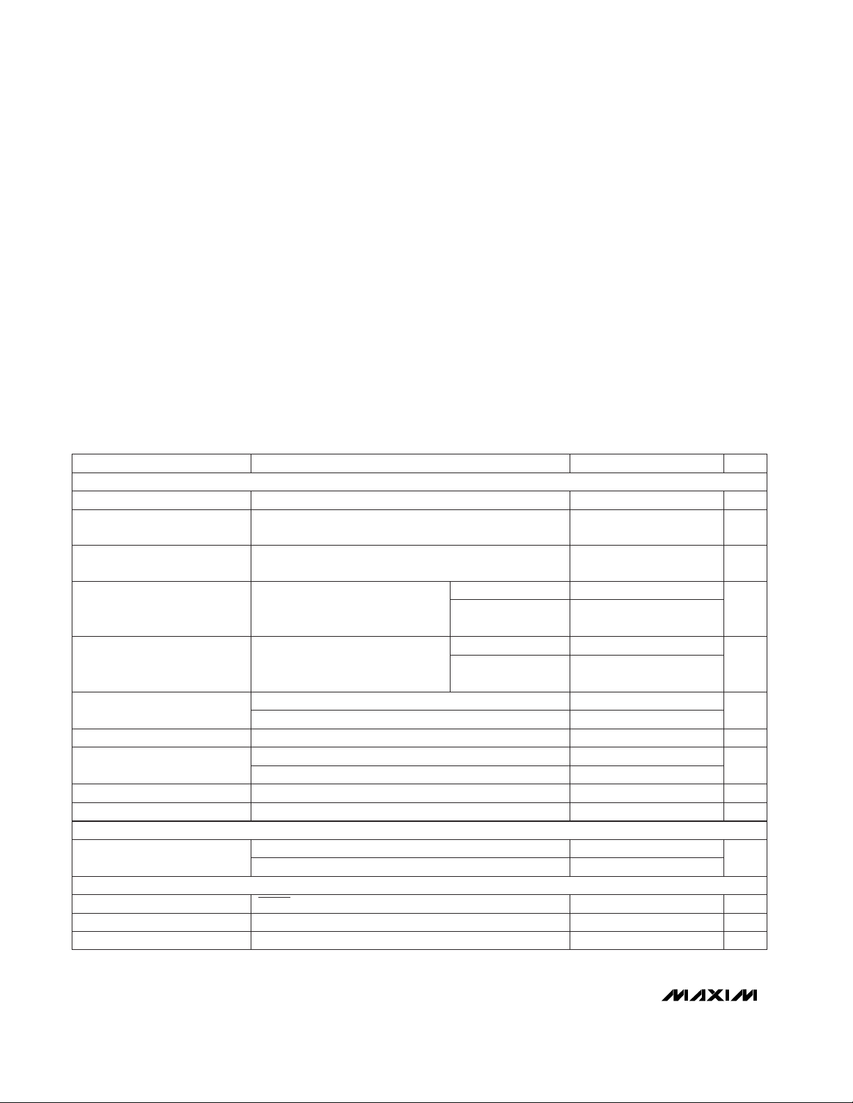
ABSOLUTE MAXIMUM RATINGS
ELECTRICAL CHARACTERISTICS
(V+ = +15V, GND = PGND = 0V, SYNC = REF, IVL= I
REF
= 0A, TA= 0°C to +85°C, unless otherwise noted.)
Stresses beyond those listed under “Absolute Maximum Ratings” may cause permanent damage to the device. These are stress ratings only, and functional
operation of the device at these or any other conditions beyond those indicated in the operational sections of the specifications is not implied. Exposure to
absolute maximum rating conditions for extended periods may affect device reliability.
V+ to GND..............................................................-0.3V to +36V
GND to PGND .......................................................-0.3V to +0.3V
VL to GND ................................................................-0.3V to +6V
BST to GND............................................................-0.3V to +36V
DH to LX.....................................................-0.3V to (BST + 0.3V)
LX to BST..................................................................-6V to +0.3V
SHDN to GND...............................................-0.3V to (V+ + 0.3V)
SYNC, SS, REF, SECFB, SKIP, FB to GND...-0.3V to (VL + 0.3V)
DL to PGND..................................................-0.3V to (VL + 0.3V)
CSH, CSL to GND ....................................................-0.3V to +6V
VL Short Circuit to GND..............................................Momentary
REF Short Circuit to GND...........................................Continuous
VL Output Current...............................................+50mA to -1mA
REF Output Current...............................................+5mA to -1mA
Continuous Power Dissipation (T
A
= +70°C)
SO (derate 8.70mW/°C above +70°C) .......................696mW
QSOP (derate 8.3mW/°C above +70°C) ....................667mW
Operating Temperature Range
MAX165_E_E ..................................................-40°C to +85°C
Storage Temperature Range.............................-65°C to +160°C
Lead Temperature (soldering, 10sec).............................+300°C
Rising edge, falling edge hysteresis = 60mV
Rising edge, falling edge hysteresis = 50mV
SHDN = 2V, 0 < IVL< 25mA, 5.5V < V+ < 30V
Rising edge, falling edge, hysteresis = 22mV (MAX1654)
CSH - CSL, negative
CSH - CSL, positive
Falling edge, rising edge, hysteresis = 22mV (MAX1652)
6V < V+ < 30V
25mV < (CSH - CSL) < 80mV
0 < (CSH - CSL) < 80mV, FB = VL, 6V < V+ < 30V,
includes line and load regulation
External resistor divider
VSS= 4V
0 < (CSH - CSL) < 80mV
VSS= 0V
CONDITIONS
V4.2 4.5 4.7VL/CSL Switchover Voltage
V3.8 3.9 4.0VL Fault Lockout Voltage
V4.7 5.0 5.3VL Output Voltage
-0.05 0 0.05
V
2.45 2.50 2.55
SECFB Regulation Setpoint
mA2.0SS Fault Sink Current
µA2.5 4.0 6.5SS Source Current
V4.5 30Input Supply Range
-50 -100 -160
mV
80 100 120
Current-Limit Voltage
%/V0.03 0.06Line Regulation
1.2
V4.85 5.06 5.255V Output Voltage (CSL)
V
1 5.5
Nominal Adjustable Output
Voltage Range
%
2
Load Regulation
UNITSMIN TYP MAXPARAMETER
0 < (CSH - CSL) < 80mV, FB = 0V, 4.5V < V+ < 30V,
includes line and load regulation
V3.20 3.34 3.463.3V Output Voltage (CSL)
2.5 5.5
MAX1655
MAX1652/MAX1653/
MAX1654
2.43 2.50 2.57
MAX1652/MAX1653/
MAX1654
CSH - CSL = 0V, CSL = FB,
SKIP = 0V, 4.5V < V+ < 30V
MAX1655
V
0.97 1.00 1.03
Feedback Voltage
3.3V AND 5V STEP-DOWN CONTROLLERS
FLYBACK/PWM CONTROLLER
INTERNAL REGULATOR AND REFERENCE
MAX1652–MAX1655
High-Efficiency, PWM, Step-Down
DC-DC Controllers in 16-Pin QSOP
_______________________________________________________________________________________ 3
Note 1: Since the reference uses VL as its supply, V+ line-regulation error is insignificant.
Note 2: At very low input voltages, quiescent supply current may increase due to excessive PNP base current in the VL linear
regulator. This occurs if V+ falls below the preset VL regulation point (5V nominal).
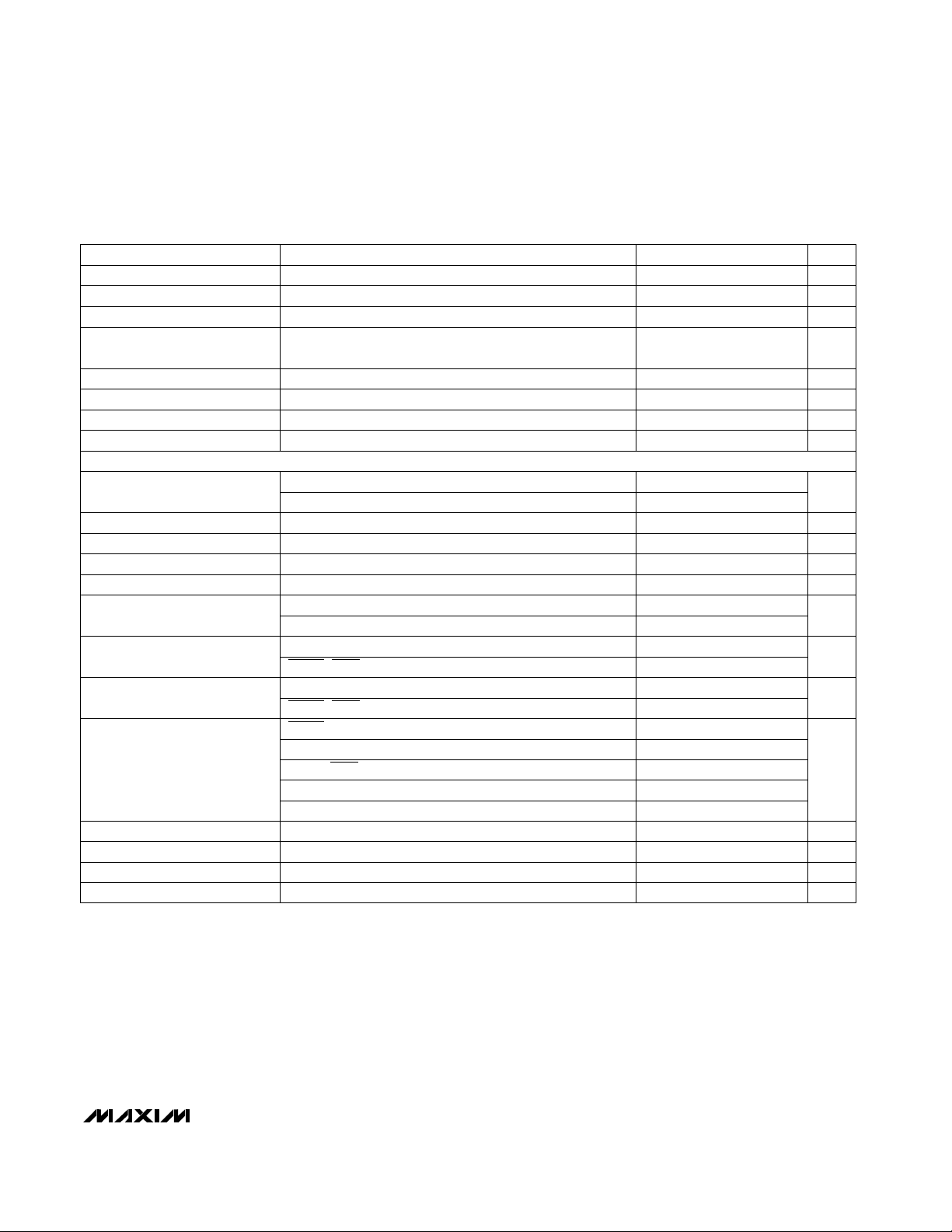
ELECTRICAL CHARACTERISTICS (continued)
(V+ = +15V, GND = PGND = 0V, SYNC = REF, IVL= I
REF
= 0A, TA= 0°C to +85°C, unless otherwise noted.)
SECFB, 0 or 4V
SHDN, 0 or 30V
SHDN, SKIP
SYNC
SYNC = 0 or 5V
SYNC = REF
Guaranteed by design, not tested
CSH = CSL = 5.5V
V+ = 4.5V, CSH = CSL = 4.0V (Note 2)
SYNC = 0 or 5V
Falling edge
0 < I
REF
< 100µA
SYNC = REF
SHDN = 0V, CSL = 5.5V, CSH = 5.5V, V+ = 0 or 30V,
VL = 0V
CONDITIONS
0.1
µA
3.0
No external load (Note 1)
Input Current
2.0
V
VL - 0.5
Input High Voltage
%
98 99
97 98
Dropout-Mode Maximum Duty
Cycle
kHz190 340Oscillator Sync Range
ns200SYNC Rise/Fall Time
ns200SYNC Low Pulse Width
ns200SYNC High Pulse Width
125 150 175
kHz
270 300 330
Oscillator Frequency
2.46 2.50 2.54
1 2Quiescent Power Consumption
1 8Dropout Power Consumption
5 15
V+ Shutdown Current
V2.0 2.4Reference Fault Lockout Voltage
mV15Reference Load Regulation
µA0.1 1
CSL, CSH Shutdown Leakage
Current
UNITSMIN TYP MAXPARAMETER
SHDN = 0V, V+ = 30V, CSL = 0 or 5.5V
FB = CSH = CSL = 5.5V, VL switched over to CSLV+ Off-State Leakage Current
DL forced to 2V
FB, FB = REF
CSH, CSL, CSH = CSL ≤ 4V
SYNC, SKIP
A1DL Sink/Source Current
±0.1
70
1.0
SHDN, SKIP
SYNC
0.5
V
0.8
Input Low Voltage
DH forced to 2V, BST - LX = 4.5V A1DH Sink/Source Current
High or low, BST - LX = 4.5V
High or low
Ω1.5 5DH On-Resistance
Ω1.5 5DL On-Resistance
Reference Output Voltage V
OSCILLATOR AND INPUTS/OUTPUTS
3 7
5 15
µA
µA
mW
mW
V
MAX1652–MAX1655
High-Efficiency, PWM, Step-Down
DC-DC Controllers in 16-Pin QSOP
4 _______________________________________________________________________________________
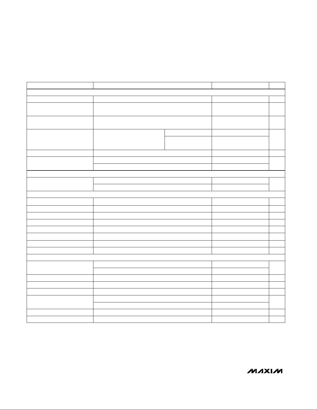
ELECTRICAL CHARACTERISTICS (continued)
(V+ = +15V, GND = PGND = 0V, SYNC = REF, IVL= I
REF
= 0A, TA= -40°C to +85°C, unless otherwise noted.) (Note 3)
Note 3: Specifications from 0°C to -40°C are guaranteed by design, not production tested.
0 < (CSH - CSL) < 70mV, FB = VL, 4.5V < V+ < 30V,
includes line and load regulation
0 < (CSH - CSL) < 70mV, FB = VL, 6V < V+ < 30V,
includes line and load regulation
CONDITIONS
V3.16 3.503.3V Output Voltage (CSL)
V4.5 30Input Supply Range
V4.80 5.305V Output Voltage (CSL)
UNITSMIN TYP MAXPARAMETER
CSH - CSL, negative
CSH - CSL, positive
-40 -160
Current-Limit Voltage
V
0.96 1.04
Feedback Voltage
2.40 2.60
mV
70 130
FB = CSH = CSL = 5.5V, VL switched over to CSL
SHDN = 0V, V+ = 30V, CSL = 0 or 5.5V
Rising edge, hysteresis = 60mV
No external load (Note 1)
0 < I
REF
< 100µA
µA15V+ Off-State Leakage Current
µA10V+ Shutdown Current
V
Rising edge, hysteresis = 50mV
SHDN = 2V, 0 < IVL< 25mA, 5.5V < V+ < 30V
4.2 4.7VL/CSL Switchover Voltage
V2.43 2.57Reference Output Voltage
Falling edge, hysteresis = 22mV (MAX1652)
Falling edge, hysteresis = 22mV (MAX1654)
mV15Reference Load Regulation
V3.75 4.05VL Fault Lockout Voltage
V4.7 5.3VL Output Voltage
2.40 2.60
V
-0.08 0.08
SECFB Regulation Setpoint
SYNC = REF
SYNC = 0 or 5V
97
kHz210 320Oscillator Sync Range
kHz
SYNC = REF
120 180
Oscillator Frequency
ns250SYNC High Pulse Width
ns250SYNC Low Pulse Width
250 350
mW2Quiescent Power Consumption
High or low, BST - LX = 4.5V
High or low
SYNC = 0 or 5V
Ω5DH On-Resistance
Ω5DL On-Resistance
%
98
Maximum Duty Cycle
CSH - CSL = 0V, 5V < V+ < 30V,
CSL = FB, SKIP = 0V
6V < V+ < 30V %/V0.06Line Regulation
3.3V and 5V STEP-DOWN CONTROLLERS
FLYBACK/PWM CONTROLLER
INTERNAL REGULATOR AND REFERENCE
OSCILLATOR AND INPUTS/OUTPUTS
MAX1652/MAX1653/
MAX1654
MAX1655
MAX1652–MAX1655
High-Efficiency, PWM, Step-Down
DC-DC Controllers in 16-Pin QSOP
_______________________________________________________________________________________ 5
SHDN
DH
+12V
OUTPUT
+5V
OUTPUT
INPUT
6V TO 30V
BST
LX
DL
PGND
CSH
CSL
SS
REF
SYNC
GND
V+
VL
FB
SECFB
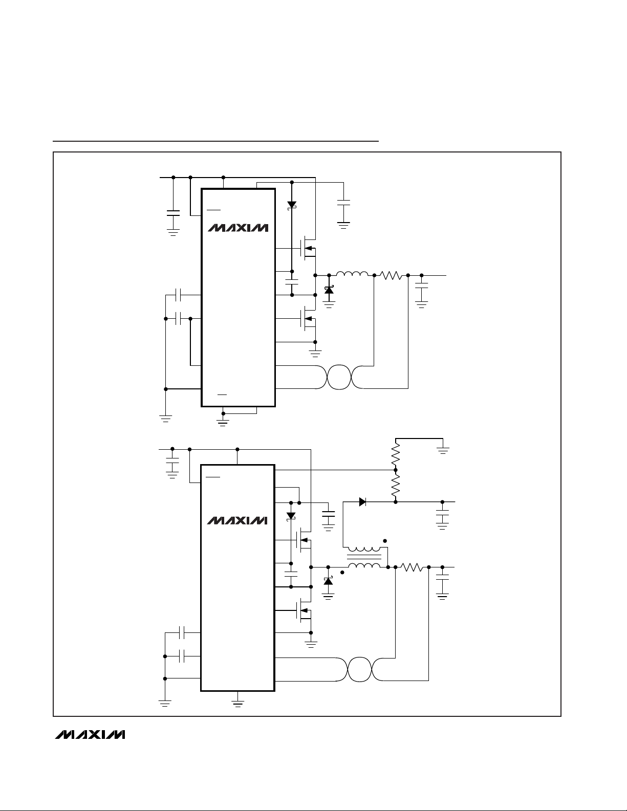
MAX1652
MAX1653
MAX1655
SHDN
DH
+3.3V
OUTPUT
INPUT
4.5V TO 30V
BST
LX
DL
PGND
CSH
CSL
SS
REF
SYNC
GND
SKIP FB
V+ VL
Typical Operating Circuits
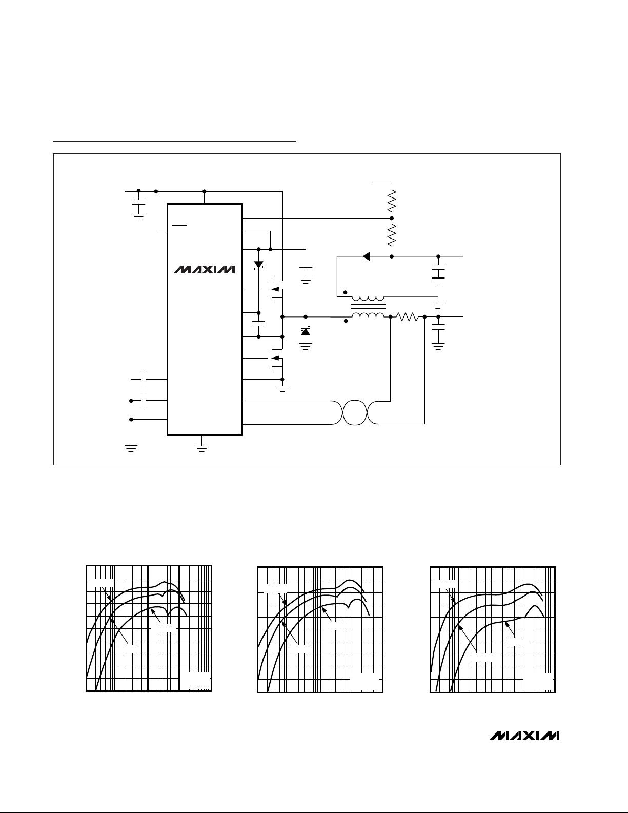
__________________________________________Typical Operating Characteristics
(Circuit of Figure 1, SKIP = GND, TA = +25°C, unless otherwise noted.)
100
50
0.001 0.1 10.01 10
EFFICIENCY vs.
LOAD CURRENT (3.3V/1A CIRCUIT)
60
MAX1652 toc01
LOAD CURRENT (A)
EFFICIENCY (%)
70
80
90
V+ = 6V
MAX1653
f = 300kHz
V+ = 28V
V+ = 12V
100
50
0.001 0.1 10.01 10
EFFICIENCY vs.
LOAD CURRENT (3.3V/2A CIRCUIT)
60
MAX1652 toc02
LOAD CURRENT (A)
EFFICIENCY (%)
70
80
90
V+ = 6V
V+ = 28V
V+ = 12V
MAX1653
f = 300kHz
100
50
0.001 0.1 10.01 10
EFFICIENCY vs.
LOAD CURRENT (3.3V/3A CIRCUIT)
60
MAX1652 toc03
LOAD CURRENT (A)
EFFICIENCY (%)
70
80
90
V+ = 6V
V+ = 28V
V+ = 12V
MAX1653
f = 300kHz
MAX1652–MAX1655
High-Efficiency, PWM, Step-Down
DC-DC Controllers in 16-Pin QSOP
6 _______________________________________________________________________________________
MAX1654
SHDN
DH
-5V
OUTPUT
+5V
OUTPUT
INPUT
6V TO 30V
BST
LX
DL
PGND
CSH
CSL
SS
REF
FROM
REF
SYNC
GND
V+
VL
FB
SECFB
Typical Operating Circuits (continued)
MAX1652–MAX1655
High-Efficiency, PWM, Step-Down
DC-DC Controllers in 16-Pin QSOP
_______________________________________________________________________________________
7
100
50
0.001 0.1 10.01 10
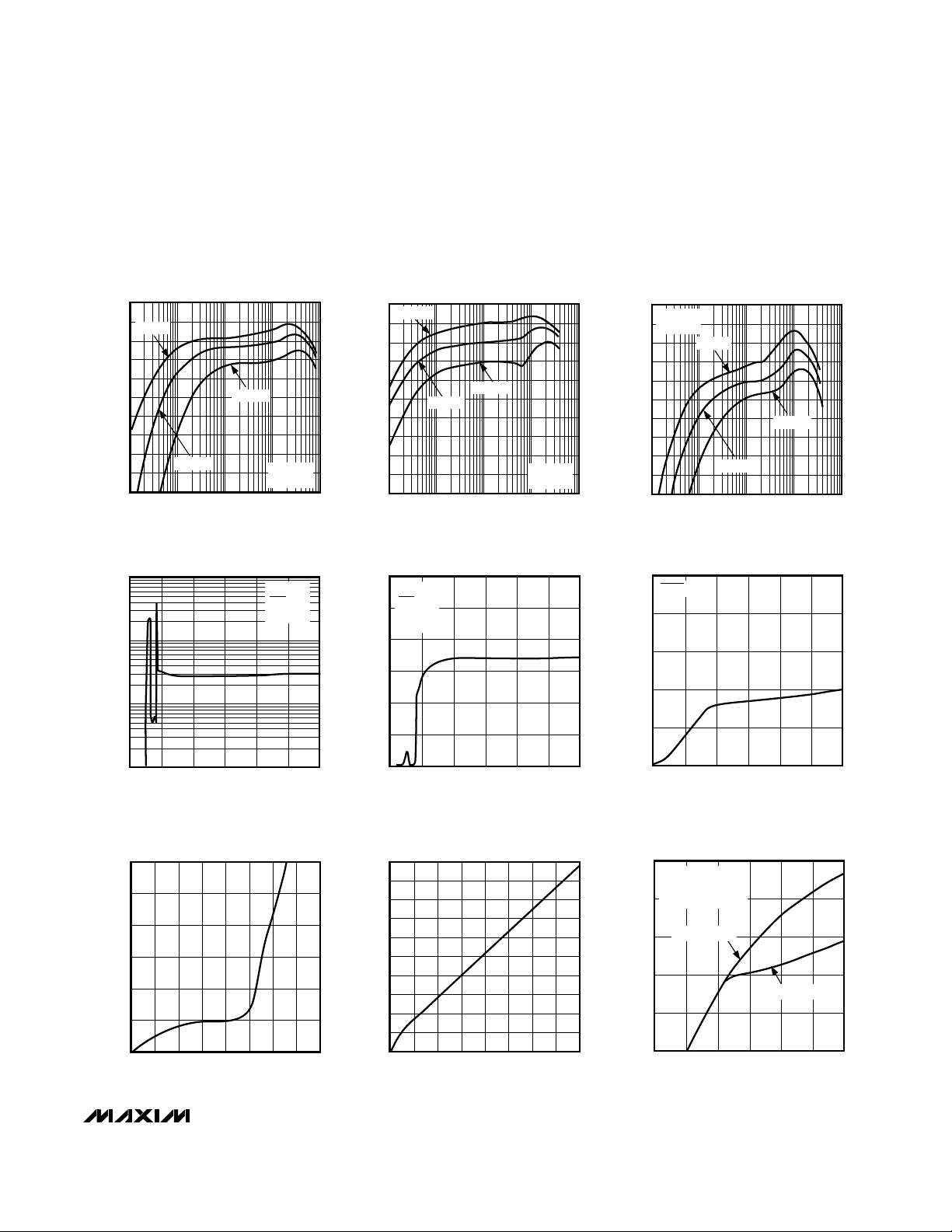
EFFICIENCY vs.
LOAD CURRENT (5V/3A CIRCUIT)
60
MAX1652 toc04a
LOAD CURRENT (A)
EFFICIENCY (%)
70
80
90
V+ = 28V
V+ = 6V
V+ = 12V
MAX1653
f = 300kHz
____________________________________Typical Operating Characteristics (continued)
(Circuit of Figure 1, SKIP = GND, TA = +25°C, unless otherwise noted.)
100
50
0.001 0.1 10.01 10
EFFICIENCY vs.
LOAD CURRENT (3.3V/5A CIRCUIT)
60
MAX1652 toc04
LOAD CURRENT (A)
EFFICIENCY (%)
70
80
90
V+ = 6V
V+ = 28V
V+ = 12V
MAX1653
f = 300kHz
0
10
5
20
15
25
30
0 10 155 20 25 30
PWM-MODE SUPPLY CURRENT vs.
INPUT VOLTAGE (3.3V/3A CIRCUIT)
MAX1652 toc07
INPUT VOLTAGE (V)
SUPPLY CURRENT (mA)
MAX1653
SKIP = VL
f = 300kHz
NO LOAD
100
50
0.001 0.1 10.01 10
EFFICIENCY vs.
LOAD CURRENT (1.8V/2.5A CIRCUIT)
60
MAX1652 toc05
LOAD CURRENT (A)
EFFICIENCY (%)
70
80
90
V+ = 6V
V+ = 24V
V+ = 12V
MAX1655
f = 300kHz
0.01
0 302010 25155
IDLE-MODE SUPPLY CURRENT vs.
INPUT VOLTAGE (3.3V/3A CIRCUIT)
0.1
1
10
MAX1652 toc06
INPUT VOLTAGE (V)
SUPPLY CURRENT (mA)
MAX1653
SKIP = 0
NO LOAD
0
4
2
6
8
10
0 10 155 20 25 30
SHUTDOWN SUPPLY CURRENT
vs. INPUT VOLTAGE
MAX1652 toc08
INPUT VOLTAGE (V)
SUPPLY CURRENT (µA)
SHDN = 0V
0
10
5
20
15
25
30
0 100 15050 200 250 300 350 400
REF LOAD-REGULATION ERROR
vs. REF LOAD CURRENT
MAX1652 toc010
LOAD CURRENT (µA)
LOAD REGULATION ∆V (mV)
0
300
900
600
1200
1500
0 10 155 20 25 30
MAX1652 MAXIMUM SECONDARY OUTPUT
CURRENT vs. SUPPLY VOLTAGE
MAX1652 toc12
SUPPLY VOLTAGE (V)
MAXIMUM SECONDARY CURRENT (mA)
V
SEC
> 12.75V,
+5V OUTPUT > 4.75V,
CIRCUIT OF FIGURE 9
+5V LOAD = 0A
+5V LOAD = 3A
0
10
5
20
15
25
50
45
40
35
30
0 20 3010 40 50 60 70 80
VL LOAD-REGULATION ERROR
vs. VL LOAD CURRENT
MAX1652 toc011
LOAD CURRENT (mA)
LOAD REGULATION ∆V (mV)
OUTPUT
VOLTAGE
LOAD
CURRENT
100mV/div,
AC
2A/div
TIME (10µs)
V
IN
= 15V, 3.3V/3A CIRCUIT
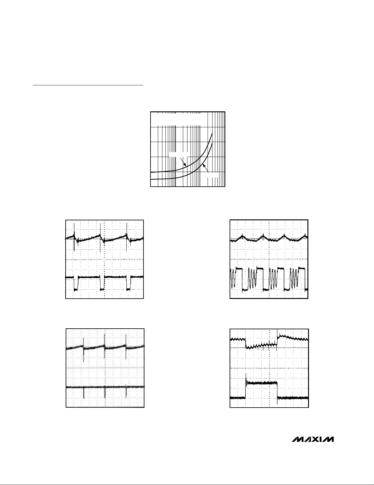
LOAD-TRANSIENT RESPONSE
MAX1652-16
OUTPUT
VOLTAGE
LX
VOLTAGE
10mV/div,
AC
5V/div
TIME (5µs)
V
IN
= 5.1V, NO LOAD, 3.3V/3A CIRCUIT,
SET TO 5V OUTPUT (FB = VL)
DROPOUT WAVEFORMS
MAX1652-15
MAX1652–MAX1655
High-Efficiency, PWM, Step-Down
DC-DC Controllers in 16-Pin QSOP
8 _______________________________________________________________________________________
OUTPUT
VOLTAGE
LX
VOLTAGE
10mV/div,
AC
5V/div
TIME (1µs)
V
IN
= 6V, 3.3V/3A CIRCUIT
PULSE-WIDTH-MODULATION
MODE WAVEFORMS
MAX1652-13
OUTPUT
VOLTAGE
LX
VOLTAGE
50mV/div,
AC
5V/div
TIME (2.5µs)
I
LOAD
= 300mA, VIN = 10V, 3.3V/3A CIRCUIT
IDLE-MODE WAVEFORMS
MAX1652-14
Typical Operating Characteristics (continued)
(Circuit of Figure 1, SKIP = GND, TA = +25°C, unless otherwise noted.)
0
0.01 1010.1
DROPOUT VOLTAGE vs.
LOAD CURRENT (3.3V/3A CIRCUIT)
100
300
400
200
500
MAX1652 toc09
LOAD CURRENT (A)
DROPOUT VOLTAGE (mV)
OUTPUT SET FOR 5V (FB = VL)
V
OUT
> 4.85V
f = 150kHz
f = 300kHz
MAX1652–MAX1655
High-Efficiency, PWM, Step-Down
DC-DC Controllers in 16-Pin QSOP
_______________________________________________________________________________________ 9
Pin Description
Dual Mode is a trademark of Maxim Integrated Products.
SKIP
(MAX1653/
MAX1655)
Disables pulse-skipping mode when high. Connect to GND for normal use. Don’t leave SKIP unconnected.
With SKIP
grounded, the device will
automatically
change from pulse-skipping operation to full PWM opera-
tion when the load current exceeds approximately 30% of maximum (Table 3).
16 DH
High-Side Gate-Drive Output. Normally drives the main buck switch. DH is a floating driver output that swings
from LX to BST, riding on the LX switching-node voltage.
15 LX Switching Node (inductor) Connection. Can swing 2V below ground without hazard.
14 BST Boost Capacitor Connection for High-Side Gate Drive (0.1µF)
13 DL Low-Side Gate-Drive Output. Normally drives the synchronous-rectifier MOSFET. Swings from 0V to VL.
NAME FUNCTION
1 SS Soft-Start Timing Capacitor Connection. Ramp time to full current limit is approximately 1ms/nF.
2
SECFB
(MAX1652/
MAX1654)
Secondary Winding Feedback Input. Normally connected to a resistor divider from an auxiliary output.
Don’t leave SECFB unconnected.
• MAX1652: SECFB regulates at VSECFB = 2.50V. Tie to VL if not used.
• MAX1654: SECFB regulates at VSECFB = 0V. Tie to a negative voltage through a high-value current-
limiting resistor (I
MAX
= 100µA) if not used.
PIN
3 REF Reference Voltage Output. Bypass to GND with 0.33µF minimum.
7 FB
Feedback Input. Regulates at the feedback voltage in adjustable mode. FB is a Dual ModeTMinput that also
selects the fixed output voltage settings as follows:
• Connect to GND for 3.3V operation.
• Connect to VL for 5V operation.
• Connect FB to a resistor divider for adjustable mode. FB can be driven with +5V CMOS logic in order to
change the output voltage under system control.
6 SHDN
Shutdown Control Input, active low. Logic threshold is set at approximately 1V (VTHof an internal N-channel
MOSFET). Tie SHDN to V+ for automatic start-up.
5 SYNC
Oscillator Synchronization and Frequency Select. Tie to GND or VL for 150kHz operation; tie to REF for
300kHz operation. A high-to-low transition begins a new cycle. Drive SYNC with 0 to 5V logic levels (see the
Electrical Characteristics
table for VIHand VILspecifications). SYNC capture range is 190kHz to 340kHz.
4 GND Low-Noise Analog Ground and Feedback Reference Point
12 PGND Power Ground
11 VL
5V Internal Linear-Regulator Output. VL is also the supply voltage rail for the chip. VL is switched to the output voltage via CSL (V
CSL
> 4.5V) for automatic bootstrapping. Bypass to GND with 4.7µF. VL can supply up
to 5mA for external loads.
10 V+
Battery Voltage Input (4.5V to 30V). Bypass V+ to PGND close to the IC with a 0.1µF capacitor. Connects to a
linear regulator that powers VL.
9 CSL Current-Sense Input, low side. Also serves as the feedback input in fixed-output modes.
8 CSH Current-Sense Input, high side. Current-limit level is 100mV referred to CSL.
