Maxim MAX1648ESE, MAX1647EAP Datasheet
19-1158; Rev 0; 12/96
Chemistry-Independent
Battery Chargers
_______________General Description
The MAX1647/MAX1648 provide the power control necessary to charge batteries of any chemistry. In the MAX1647,
all charging functions are controlled via the Intel System
Management Bus (SMBus™) interface. The SMBus 2-wire
serial interface sets the charge voltage and current, and
provides thermal status information. The MAX1647 functions as a level 2 charger, compliant with the Duracell/Intel
Smart Battery Charger Specification. The MAX1648 omits
the SMBus serial interface, and instead sets the charge
voltage and current proportional to the voltage applied to
external control pins.
In addition to the feature set required for a level 2 charger,
the MAX1647 generates interrupts to signal the host when
power is applied to the charger or a battery is installed or
removed. Additional status bits allow the host to check
whether the charger has enough input voltage, and
whether the voltage on or current into the battery is being
regulated. This allows the host to determine when lithiumion batteries have completed charge without interrogating
the battery.
The MAX1647 is available in a 20-pin SSOP with a 2mm
profile height. The MAX1648 is available in a 16-pin SO
package.
________________________Applications
Notebook Computers
Personal Digital Assistants
Charger Base Stations
Phones
____________________________Features
♦ Charges Any Battery Chemistry:
Li-Ion, NiCd, NiMH, Lead Acid, etc.
♦ Intel SMBus 2-Wire Serial Interface (MAX1647)
♦ Intel/Duracell Level 2 Smart Battery Compliant
(MAX1647)
♦ 4A, 2A, or 1A Maximum Battery-Charge Current
♦ 11-Bit Control of Charge Current
♦ Up to 18V Battery Voltage
♦ 10-Bit Control of Voltage
♦ ±0.75% Voltage Accuracy with External ±0.1%
Reference
♦ Up to 28V Input Voltage
♦ Battery Thermistor Fail-Safe Protection
______________Ordering Information
PART
MAX1647EAP
MAX1648ESE
TEMP. RANGE PIN-PACKAGE
-40°C to +85°C
-40°C to +85°C
20 SSOP
16 Narrow SO
MAX1647/MAX1648
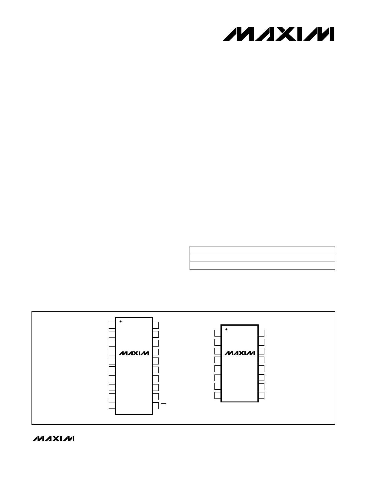
__________________________________________________________Pin Configurations
TOP VIEW
IOUT
DCIN
CCV
CCI
SEL
BATT
REF
1
2
3
VL
4
MAX1647
5
6
CS
7
8
9
10
SSOP
20
BST
16
DCIN
CCV
CCI
BATT
REF
AGND
1
VL
2
3
MAX1648
4
CS
5
6
7
8
SO
LX
19
18
DHI
17
DLO
PGND
16
15
DACV
SDA
14
SCL
13
12
THM
11
INTAGND
BST
LX
15
DHI
14
13
DLO
PGND
12
SETV
11
SETI
10
THM
9
SMBus is a trademark of Intel Corp.
________________________________________________________________
Maxim Integrated Products
1
For free samples & the latest literature: http://www.maxim-ic.com, or phone 1-800-998-8800
Chemistry-Independent
Battery Chargers
ABSOLUTE MAXIMUM RATINGS
DCIN to AGND..........................................................-0.3V to 30V
DCIN to IOUT...........................................................-0.3V to 7.5V
BST to AGND............................................................-0.3V to 36V
BST, DHI to LX............................................................-0.3V to 6V
LX to AGND ..............................................................-0.3V to 30V
THM, CCI, CCV, DACV, REF,
DLO to AGND................................................-0.3V to (VL + 0.3V)
VL, SEL, INT, SDA, SCL to AGND (MAX1647) ...........-0.3V to 6V
SETV, SETI to AGND (MAX1648)................................-0.3V to 6V
BATT, CS+ to AGND.................................................-0.3V to 20V
Stresses beyond those listed under “Absolute Maximum Ratings” may cause permanent damage to the device. These are stress ratings only, and functional
operation of the device at these or any other conditions beyond those indicated in the operational sections of the specifications is not implied. Exposure to
absolute maximum rating conditions for extended periods may affect device reliability.
ELECTRICAL CHARACTERISTICS
(V
DCIN
= 18V, V
= 4.096V, TA= 0°C to +85°C. Typical values are at TA= +25°C, unless otherwise noted.)
REF
PGND to AGND.....................................................-0.3V to +0.3V
SDA, INT Current ................................................................50mA
VL Current...........................................................................50mA
Continuous Power Dissipation (T
16-Pin SO (derate 8.7mW/°C above +70°C).................696mW
20-Pin SSOP (derate 8mW/°C above +70°C) ...............640mW
Operating Temperature Range
MAX1647EAP, MAX1648ESE ...........................-40°C to +85°C
Storage Temperature.........................................-60°C to +150°C
Lead Temperature (soldering, 10sec).............................+300°C
= +70°C)
A
MAX1647/MAX1648
SUPPLY AND REFERENCE
LOAD
SWITCHING REGULATOR
BATT Input Current (Note 1)
CS Input Current (Note 1)
CS to BATT Single-Count
Current-Sense Voltage
CS to BATT Full-Scale
Current-Sense Voltage
Voltage Accuracy
MAX1647, SEL = open,
ChargingCurrent( ) = 0x0020
MAX1647, SEL = open,
ChargingCurrent( ) = 0x07F0;
MAX1648, V
MAX1647, ChargingVoltage( ) = 0x1060,
ChargingVoltage( ) = 0x3130; MAX1648,
V
SETV
< 28V, logic inputs = VLDCIN Quiescent Current
DCIN
< 28V, no loadVL Output Voltage
DCIN
= 10mAVL Load Regulation
SOURCE
BATT
BATT
SETI
= 3.15V, V
< 500µAREF Output Voltage
= 12V
= 12V
= 1.024V
SETV
= 1.05V
15VL < 3.2V, V
350 500VL < 5.15V, V
15VL < 3.2V, VCS= 12V
170 400VL < 5.15V, VCS= 12V
-0.65 0.65
UNITSMIN TYP MAXCONDITIONSPARAMETER
V7.5 28DCIN Input Voltage Range
mA467.5V < V
V5.15 5.4 5.657.5V < V
mV100I
V3.20 4 5.15MAX1647VL AC_PRESENT Trip Point
V3.74 3.9 4.070µA < I
µA700REF Overdrive Input Current
kHz200 250 300Oscillator Frequency
%89 93DHI Maximum Duty Cycle
Ω47High or lowDHI On-Resistance
Ω614High or lowDLO On-Resistance
µA
µA
V019BATT, CS Input Voltage Range
mV2.94
mV170 185 200
%
2 _______________________________________________________________________________________
Chemistry-Independent
Battery Chargers
ELECTRICAL CHARACTERISTICS (continued)
(V
= 18V, V
DCIN
ERROR AMPLIFIERS
GMV Amplifier Maximum
Output Current
GMI Amplifier Maximum
Output Current
CCI Clamp Voltage with
Respect to CCV
CCV Clamp Voltage with
Respect to CCI
TRIP POINTS AND LINEAR CURRENT SOURCES
THM THERMISTOR_OR
Over-Range Trip Point
THM THERMISTOR_COLD
Trip Point
THM THERMISTOR_HOT
Trip Point
THM THERMISTOR_UR
Under-Range Trip Point
IOUT Output Current
CURRENT- AND VOLTAGE-SETTING DACs (MAX1647)
SETV, SETI (MAX1648)
LOGIC LEVELS (MAX1647)
Note 1: When DCIN is less than 4V, VL is less than 3.2V, causing the battery current to be typically 2µA (CS plus BATT input
current).
= 4.096V, TA= 0°C to +85°C. Typical values are at TA= +25°C, unless otherwise noted.)
REF
< 3.5V
CCV
< 3.5V
CCI
86.5 89 91.5MAX1647BATT POWER_FAIL Trip Point
89.5 91 92.5MAX1647
74 75.5 77
22 23.5 25
3 4.5 6MAX1647
MAX1647,
V
= 7.5V,
DCIN
V
= 0V
IOUT
= 0.6VSDA Output Low Sink Current
SDA
ChargingCurrent( ) = 0x001F
ChargingCurrent( ) = 0x0000 10 µA
UNITSMIN TYP MAXCONDITIONSPARAMETER
mA/V1.4GMV Amplifier Transconductance
mA/V0.2GMI Amplifier Transconductance
V
µA±80
µA±200
mV25 80 2001.1V < V
mV25 80 2001.1V < V
% of
DCIN
% of
V
REF
% of
V
REF
% of
V
REF
% of
V
REF
mA25 31 35
V-7.5 -1.0With respect to DCIN voltageIOUT Operating Voltage Range
bits6Guaranteed monotonicCDAC Current-Setting DAC Resolution
bits10Guaranteed monotonicVDAC Voltage-Setting DAC Resolution
µA1SETV Input Bias Current
µA5SETI Input Bias Current
V0 4.2SETV Input Voltage Range
V0 1.024SETI Input Voltage Range
V0.8SDA, SCL Input Low Voltage
V2.8SDA, SCL Input High Voltage
µA-1 1SDA, SCL Input Bias Current
mA6V
MAX1647/MAX1648
_______________________________________________________________________________________ 3
Chemistry-Independent
Battery Chargers
ELECTRICAL CHARACTERISTICS
(V
= 18V, V
DCIN
temperature range are guaranteed by design.)
SUPPLY AND REFERENCE
SWITCHING REGULATOR
MAX1647/MAX1648
CS to BATT Full-Scale
Current-Sense Voltage
Voltage Accuracy
ERROR AMPLIFIERS
GMV Amplifier Maximum
Output Current
GMI Amplifier Maximum
Output Current
TRIP POINTS AND LINEAR CURRENT SOURCES
THM THERMISTOR_OR
Over-Range Trip Point
THM THERMISTOR_COLD
Trip Point
THM THERMISTOR_HOT
Trip Point
THM THERMISTOR_UR
Under-Range Trip Point
SETV, SETI (MAX1648)
LOGIC LEVELS (MAX1647)
= 4.096V, TA= -40°C to +85°C. Typical values are at TA= +25°C, unless otherwise noted. Limits over this
REF
< 28V, logic inputs = VLDCIN Quiescent Current
DCIN
< 28V, no loadVL Output Voltage
DCIN
SOURCE
BATT
MAX1647, SEL = open,
ChargingCurrent( ) = 0x07F0;
MAX1648, V
MAX1647, ChargingVoltage( ) = 0x1060,
ChargingVoltage( ) = 0x3130; MAX1648,
V
SETV
SDA
SETI
= 3.15V, V
= 0.6VSDA Output Low Sink Current
< 500µAREF Output Voltage
= 12V
= 1.024V
SETV
= 1.05V
89.5 91 92.5MAX1647
74 75.5 77
22 23.5 25
3 4.5 6MAX1647
UNITSMIN TYP MAXCONDITIONSPARAMETER
mA/V1.4GMV Amplifier Transconductance
mA/V0.2GMI Amplifier Transconductance
mA467.5V < V
V5.15 5.4 5.657.5V < V
V3.74 3.9 4.070µA < I
kHz200 250 310Oscillator Frequency
%89DHI Maximum Duty Cycle
Ω47High or lowDHI On-Resistance
Ω614High or lowDLO On-Resistance
µABATT Input Current 5VL < 3.2V, V
µACS Input Current 5VL < 3.2V, VCS= 12V
mV160 185 200
%-0.65 0.65
µA±130
µA±320
% of
V
REF
% of
V
REF
% of
V
REF
% of
V
REF
µA1SETV Input Bias Current
µA5SETI Input Bias Current
V0.8SDA, SCL Input Low Voltage
V2.8SDA, SCL Input High Voltage
µA-1 1SDA, SCL Input Bias Current
mA6V
4 _______________________________________________________________________________________
Chemistry-Independent
Battery Chargers
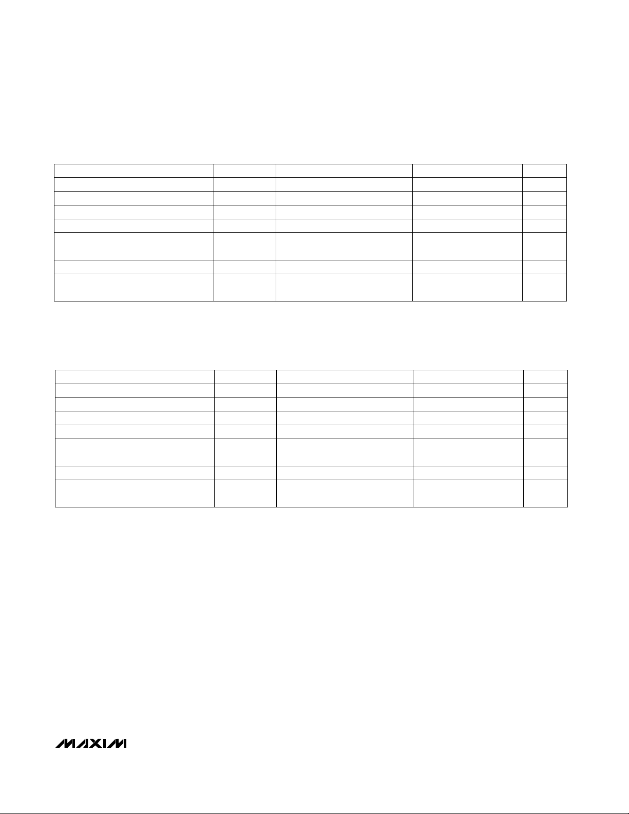
TIMING CHARACTERISTICS—MAX1647
(TA= 0°C to +85°C, unless otherwise noted.)
SCL Serial-Clock High Period
SCL Serial-Clock Low Period
Start-Condition Setup Time
Start-Condition Hold Time
SDA Valid to SCL Rising-Edge
Setup Time, Slave Clocking in Data
SCL Falling Edge to SDA Transition
SCL Falling Edge to SDA Valid,
Master Clocking in Data
HIGH
LOW
SU:STA
HD:STA
SU:DAT
HD:DAT
DV
TIMING CHARACTERISTICS—MAX1647
(TA= -40°C to +85°C, unless otherwise noted. Limits over this temperature range are guaranteed by design.)
CONDITIONS
SCL Serial-Clock High Period
SCL Serial-Clock Low Period
Start-Condition Setup Time
Start-Condition Hold Time
SDA Valid to SCL Rising-Edge
Setup Time, Slave Clocking in Data
SCL Falling Edge to SDA Transition
SCL Falling Edge to SDA Valid,
Master Clocking in Data
HIGH
LOW
SU:STA
HD:STA
SU:DAT
HD:DAT
DV
MAX1647/MAX1648
UNITSMIN TYP MAXSYMBOLPARAMETER CONDITIONS
µs4t
µs4.7t
µs4.7t
µs4t
ns250t
ns0t
µs1t
UNITSMIN TYP MAXSYMBOLPARAMETER
µs4t
µs4.7t
µs4.7t
µs4t
ns250t
ns0t
µs1t
_______________________________________________________________________________________ 5
Chemistry-Independent
Battery Chargers
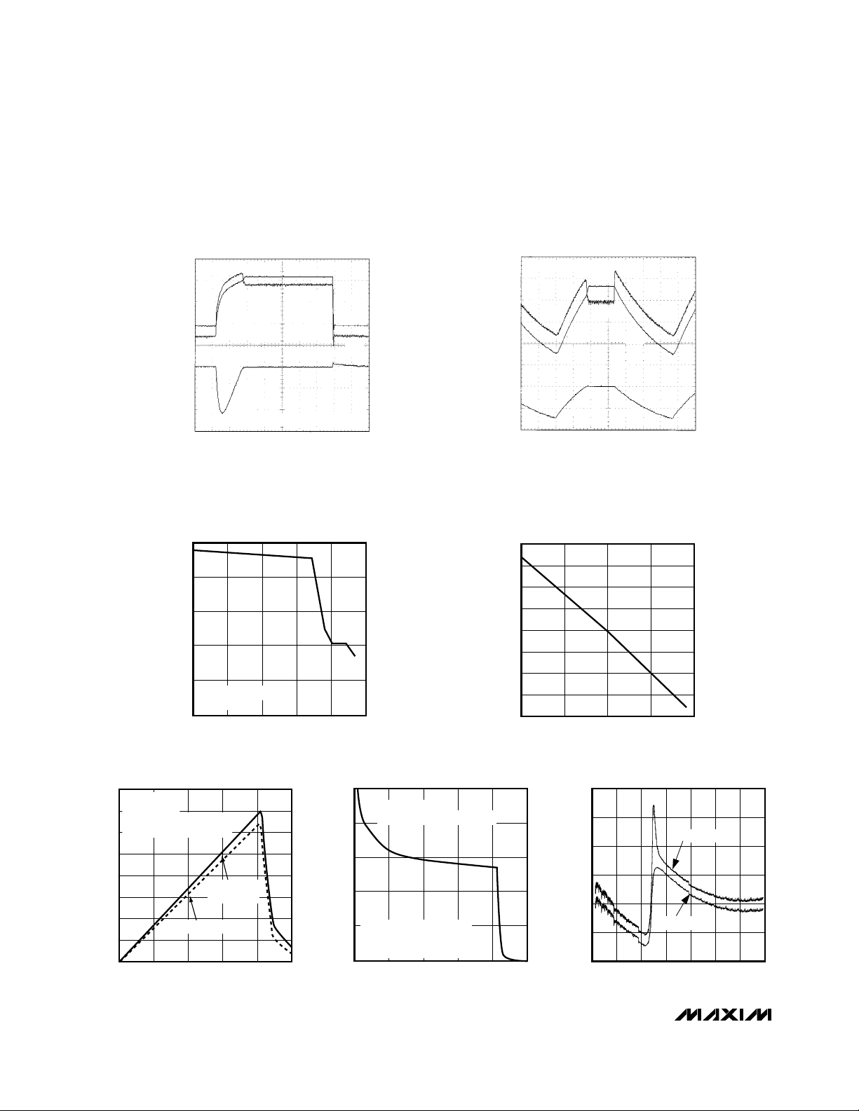
__________________________________________Typical Operating Characteristics
(Circuit of Figure 3, TA = +25°C, unless otherwise noted.)
MAX1647
BATT LOAD TRANSIENT
CCI
CCV
0.9A TO 1.9A TO 0.9A
1ms/div
MAX1647/MAX1648
ChargingVoltage( ) = 0x2EE0 = 12000mV
ChargingCurrent( ) = 0xFFFF = MAX VALUE
ACDCIN = 18.0V, SEL = OPEN, R1 = 0.1Ω
R2 = 10kΩ, C1 = 68µF, C2 = 0.1µF, C3 = 47nF
L1 = 22µH, V
= 4.096V
REF
VL VOLTAGE vs. LOAD CURRENT
5.5
5.0
4.5
VL (V)
4.0
3.5
CIRCUIT OF FIGURE 3
= 6.6V
V
DCIN
0
050
10 20 40
LOAD CURRENT (mA)
30
INPUT AND OUTPUT POWER
40
V
= 28V
DCIN
= 12.6V
V
BATT
35
ChargingCurrent( ) = 0xFFFF
ChargingVoltage( ) = 0xFFFF
30
25
20
POWER (W)
15
10
5
0
500
0 2500
CURRENT INTO BATT (mA)
POWER INTO
CIRCUIT
POWER TO BATT
1000 1500
2000
0.001
MAX1647/48-05
0.01
0.1
DROP IN BATT OUTPUT VOLTAGE (%)
100
MAX1647/48-01
V
2.4V
12V
MAX1647/48-03
CCI
V
CCV
200mV/div
V
BATT
1V/div
CCI
CCV
MAX1647
OUTPUT V-I CHARACTERISTIC
BATT NO-LOAD
OUTPUT VOLTAGE = 16.384V
1
10
V
= 28V, V
DCIN
ChargingVoltage( ) = 0xFFFF
ChargingCurrent( ) = 0xFFFF
500 1000 2000
0 2500
= 4.096V
REF
1500
LOAD CURRENT (mA)
1.1A TO 0.9A TO 1.1A
CCV
ChargingVoltage( ) = 0x2EE0 = 12000mV
ChargingCurrent( ) = 0x03E8 = 1000mA
ACDCIN = 18.0V, SEL = OPEN, C1 = 68µF,
C2 = 0.1µF, C3 = 47nF, R1 = 0.1Ω
R2 = 10kΩ, L1 = 22µH, V
INTERNAL REFERENCE VOLTAGE
3.86
3.84
3.82
3.80
(V)
3.78
REF
V
3.76
3.74
3.72
3.70
0 2.0
MAX1647/48-06
MAX1647
BATT LOAD TRANSIENT
CCI
CCV
CCI
2ms/div
REF
0.5 1.0 1.5
LOAD CURRENT (mA)
MAX1647/48-02
CCV
CCI
= 4.096V
OUTPUT VOLTAGE ERROR
0.8
0.6
0.4
0.2
0
OUTPUT VOLTAGE ERROR (%)
-0.2
-0.4
4500 8500 12,500
PROGRAMMED VOLTAGE CODE IN DECIMAL
3mA LOAD
300mA LOAD
2.3V
12V
MAX1647/48-04
V
CCV
V
CCI
100mV/div
V
BATT
5V/div
16,500
MAX1647/48-07
6 _______________________________________________________________________________________
Chemistry-Independent
Battery Chargers
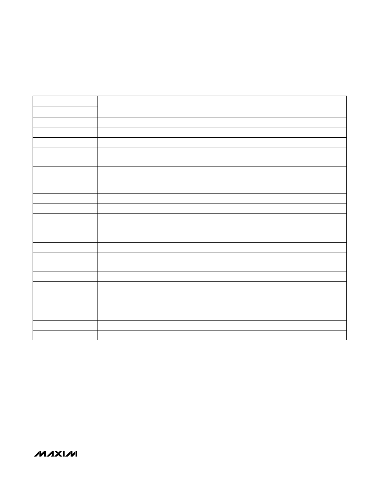
______________________________________________________________Pin Description
PIN
MAX1647 MAX1648
—6 SEL
NAME
INT
Linear Current-Source Output—1 IOUT
Input Voltage for Powering Charger12 DCIN
Chip Power Supply. 5.4V linear regulator output from DCIN.23 VL
Voltage-Regulation-Loop Compensation Point34 CCV
Current-Regulation-Loop Compensation Point45 CCI
Current-Range Selector. Tying SEL to VL sets a 4A full-scale current. Leaving SEL open
sets a 2A full-scale current. Tying SEL to AGND sets a 1A full-scale current.
Current-Sense Positive Input57 CS
Battery Voltage Input and Current-Sense Negative Input68 BATT
3.9V Reference Voltage Output or External Reference Input79 REF
Analog Ground810 AGND
Current-Regulation-Loop Set Point10— SETI
Open-Drain Interrupt Output—11
Voltage-Regulation-Loop Set Point11— SETV
Thermistor Sense Voltage Input912 THM
Serial Clock—13 SCL
Serial Data—14 SDA
Voltage DAC Output—15 DACV
Power Ground1216 PGND
Low-Side Power MOSFET Driver Output1317 DLO
High-Side Power MOSFET Driver Output1418 DHI
Power Connection for the High-Side Power MOSFET Driver1519 LX
Power Connection for the High-Side Power MOSFET Driver1620 BST
FUNCTION
MAX1647/MAX1648
_______________________________________________________________________________________ 7
Chemistry-Independent
Battery Chargers
MOST SIGNIFICANT
SCL
START
CONDITION
ADDRESS BIT (A6)
CLOCKED INTO SLAVE
A5 CLOCKED
INTO SLAVE
A4 CLOCKED
INTO SLAVE
A3 CLOCKED
INTO SLAVE
t
HD:STA
SDA
MAX1647/MAX1648
t
SU:STA
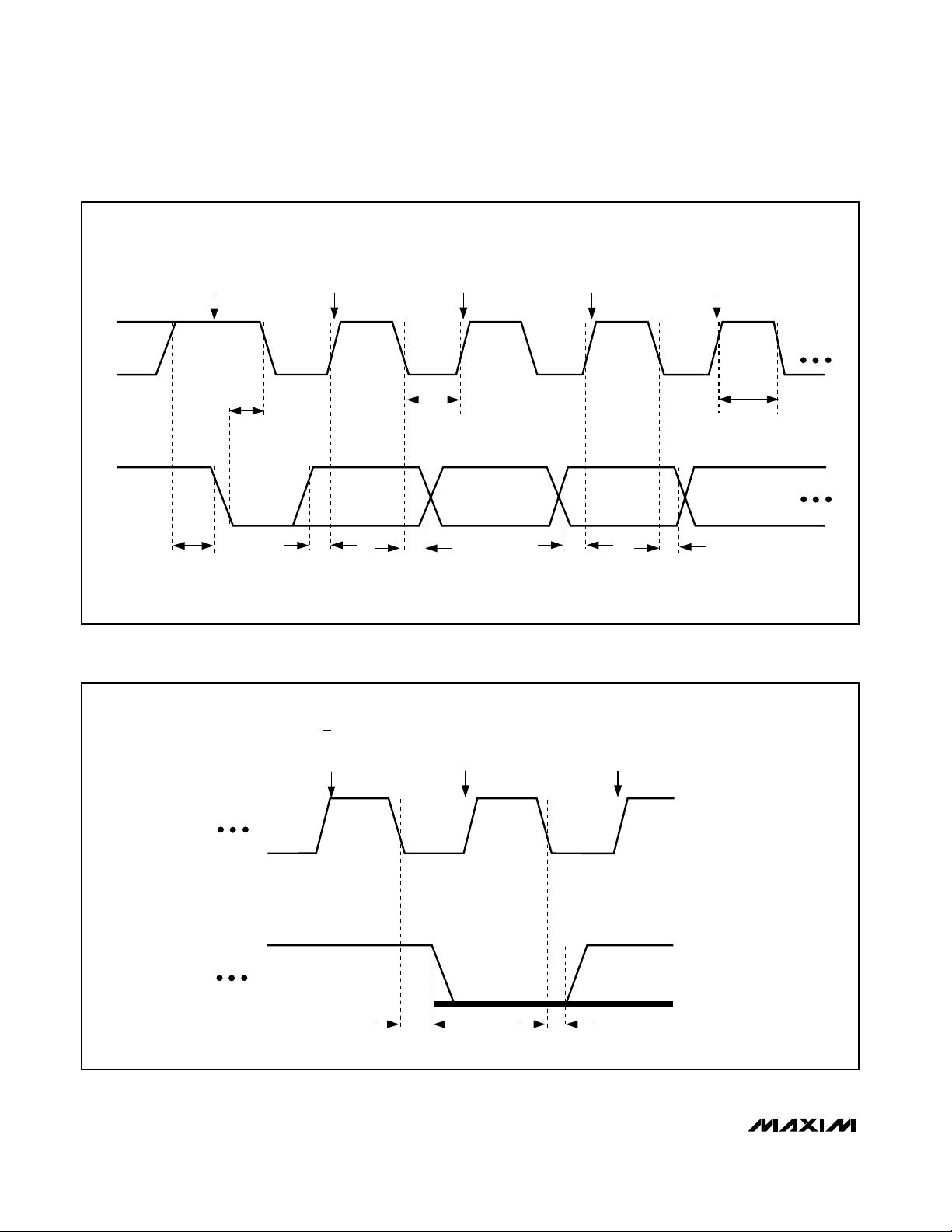
Figure 1. SMBus Serial Interface Timing—Address
SCL
t
SU:DAT
RW BIT
CLOCKED
INTO SLAVE
t
HD:DAT
t
LOW
ACKNOWLEDGE
BIT CLOCKED
INTO MASTER
t
SU:DAT
MOST SIGNIFICANT BIT
OF DATA CLOCKED
INTO MASTER
t
HD:DAT
t
HIGH
DV
SLAVE PULLING
SDA LOW
t
DV
SDA
t
Figure 2. SMBus Serial Interface Timing—Acknowledge
8 _______________________________________________________________________________________
 Loading...