Maxim MAX1645EEI Datasheet
For free samples & the latest literature: http://www.maxim-ic.com, or phone 1-800-998-8800.
For small orders, phone 1-800-835-8769.
General Description
The MAX1645 is a high-efficiency battery charger
capable of charging batteries of any chemistry type. It
uses the Intel System Management Bus (SMBus) to
control voltage and current charge outputs.
When charging lithium-ion (Li+) batteries, the MAX1645
automatically transitions from regulating current to regulating voltage. The MAX1645 can also limit line input
current so as not to exceed a predetermined current
drawn from the DC source. A 175sec charge safety
timer prevents “runaway charging” should the
MAX1645 stop receiving charging voltage/current commands.
The MAX1645 employs a next-generation synchronous
buck control circuitry that lowers the minimum input-tooutput voltage drop by allowing the duty cycle to
exceed 99%. The MAX1645 can easily charge one to
four series Li+ cells.
Applications
Notebook Computers
Point-of-Sale Terminals
Personal Digital Assistants
Features
♦ Input Current Limiting
♦ 175sec Charge Safety Timeout
♦ 128mA Wake-Up Charge
♦ Charges Any Chemistry Battery:
Li+, NiCd, NiMH, Lead Acid, etc.
♦ Intel SMBus 2-Wire Serial Interface
♦ Compliant with Level 2 Smart Battery Charger
Spec. Rev. 1.0
♦ +8V to +28V Input Voltage Range
♦ Up to 18.4V Battery Voltage
♦ 11-Bit Battery Voltage Setting
♦ ±0.8% Output Voltage Accuracy with Internal
Reference
♦ 3A max Battery Charge Current
♦ 6-Bit Charge Current Setting
♦ 99.99% max Duty Cycle for Low-Dropout Operation
♦ Load/Source Switchover Drivers
♦ >97% Efficiency
MAX1645
Advanced Chemistry-Independent, Level 2
Battery Charger with Input Current Limiting
________________________________________________________________
Maxim Integrated Products
1
19-1566; Rev 0a; 10/99
PART
MAX1645EEI -40°C to +85°C
TEMP. RANGE PIN-PACKAGE
28 QSOP
Typical Operating Circuit appears at end of data sheet.
SMBus is a trademark of Intel Corp.
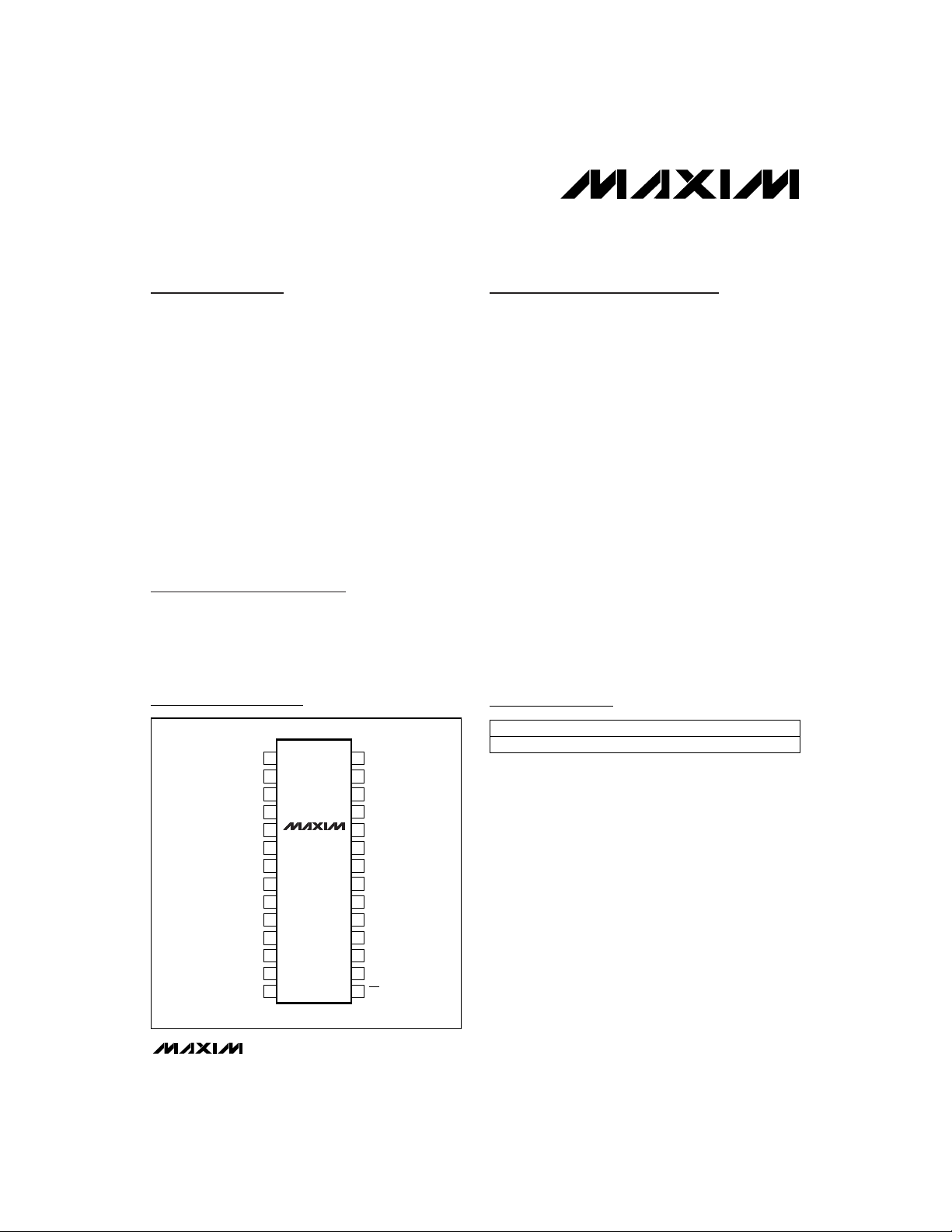
Pin Configuration
Ordering Information
TOP VIEW
1
DCIN
2
LDO
3
CLS
4
REF
5
CCS
6
CCI
7
CCV
8
GND
9
BATT
10
DAC
11
V
DD
12
THM
13
SCL
14
SDA
MAX1645
QSOP
28
27
26
25
24
23
22
21
20
19
18
17
16
15
CVS
PDS
CSSP
CSSN
BST
DHI
LX
DLOV
DLO
PGND
CSIP
CSIN
PDL
INT
MAX1645
Advanced Chemistry-Independent, Level 2
Battery Charger with Input Current Limiting
2 _______________________________________________________________________________________
ABSOLUTE MAXIMUM RATINGS
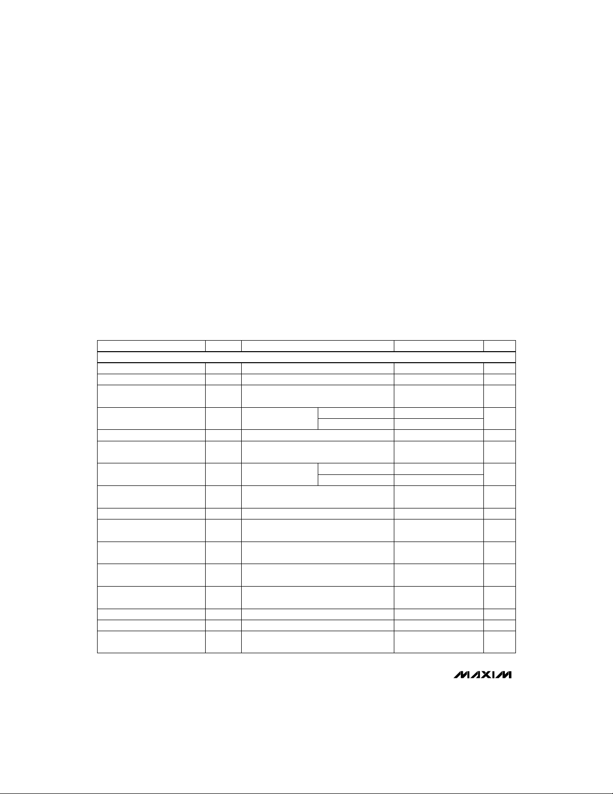
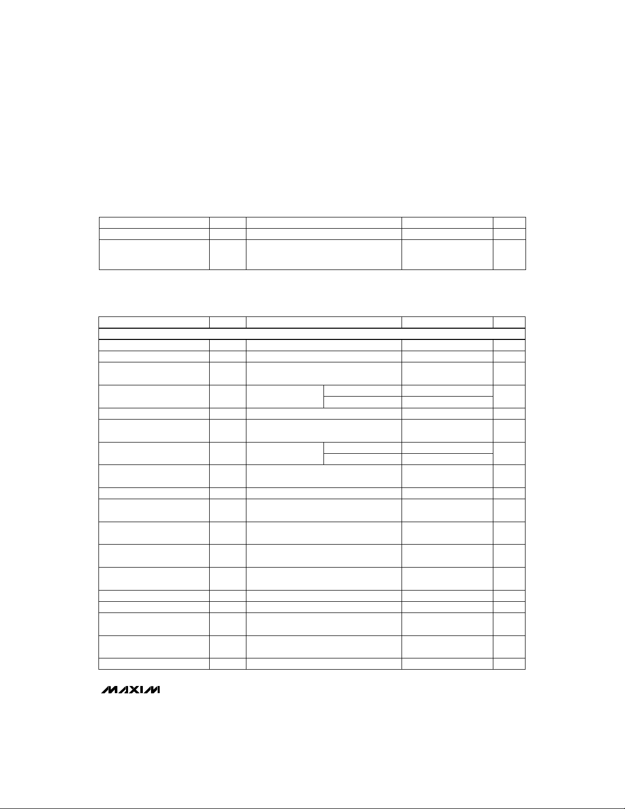
ELECTRICAL CHARACTERISTICS
(Circuit of Figure 1, VDD= +3.3V, V
BATT
= +16.8V, V
DCIN
= +18V, TA= 0°C to +85°C, unless otherwise noted. Typical values are at
T
A
= +25°C.)
Stresses beyond those listed under “Absolute Maximum Ratings” may cause permanent damage to the device. These are stress ratings only, and functional
operation of the device at these or any other conditions beyond those indicated in the operational sections of the specifications is not implied. Exposure to
absolute maximum rating conditions for extended periods may affect device reliability.
DCIN, CVS, CSSP, CSSN, LX to GND....................-0.3V to +30V
CSSP to CSSN, CSIP to CSIN ...............................-0.3V to +0.3V
PDS, PDL to GND ...................................-0.3V to (V
CSSP
+ 0.3V)
BST to LX..................................................................-0.3V to +6V
DHI to LX...................................................-0.3V to (V
BST
+ 0.3V)
CSIP, CSIN, BATT to GND .....................................-0.3V to +22V
LDO to GND.....................-0.3V to (lower of 6V or V
DCIN
+ 0.3V)
DLO to GND ...........................................-0.3V to (V
DLOV
+ 0.3V)
REF, DAC, CCV, CCI, CCS, CLS to GND.....-0.3V to (V
LDO
+ 0.3V)
V
DD
, SCL, SDA, INT, DLOV to GND.........................-0.3V to +6V
THM to GND...............................................-0.3V to (V
DD
+ 0.3V)
PGND to GND .......................................................-0.3V to +0.3V
LDO Continuous Current.....................................................50mA
Continuous Power Dissipation (T
A
= +70°C)
28-Pin QSOP (derate 10.8mW/°C above +70°C).......860mW
Operating Temperature Range ...........................-40°C to +85°C
Storage Temperature.........................................-60°C to +150°C
Lead Temperature (soldering, 10sec).............................+300°C
8V < V
DCIN
< 28V
V
CVS
referred to V
BATT
, V
CVS
rising
V
PDS
= V
CSSP
- 2V, V
DCIN
= 16V
PDS = CSSP
I
PDS
= 0
0 < V
DCIN
< 6V, VDD= 5V, V
SCL
= 5V,
V
SDA
= 5V
V
CVS
referred to V
BATT
V
CVS
referred to V
BATT
, V
CVS
falling
When the SMB responds to commands
8V < V
DCIN
< 28V
8V < V
DCIN
< 28V
When AC_PRESENT
switches
When I
CHARGE
drops to 128mA
8V < V
DCIN
< 28V, 0 < I
LDO
< 15mA
0 < I
REF
< 200µA
CONDITIONS
mV
-150 -100 -50
V
PDL-OFF
PDL Load Switch Turn-Off
Threshold
mA
10 50
PDS Turn-Off Current
µA
100 150 300
PDS Turn-On Current
V
81012
PDS Output Low Voltage, PDS
Below CSSP
mV
100 200 300
V
PDS-HYS
PDS Charging Source Switch
Threshold Hysteresis
mV
50 100 150
V
PDS-OFF
PDS Charging Source Switch
Turn-Off Threshold
V
2.4 2.8
BATT Undervoltage Threshold
(Note 2)
V
4.066 4.096 4.126
V
REF
REF Output Voltage
mA
1.7 6
I
DCIN
DCIN Supply Current
V
828
V
DCIN
µA
80 150
I
DD
VDDQuiescent Current
2.1 2.5
V
2.55 2.8
VDDUndervoltage Threshold
V
2.8 5.65
VDDInput Voltage Range
(Note 1)
mA
0.7 2
DCIN Supply Current Charging
Inhibited
V
7.5 7.85
DCIN Undervoltage Threshold
7 7.4
V
5.15 5.4 5.65
V
LDO
LDO Output Voltage
UNITSMIN TYP MAXSYMBOLPARAMETER
DCIN rising
DCIN falling
VDDrising
VDDfalling
DCIN Typical Operating Range
GENERAL SPECIFICATIONS
MAX1645
Advanced Chemistry-Independent, Level 2
Battery Charger with Input Current Limiting
_______________________________________________________________________________________ 3
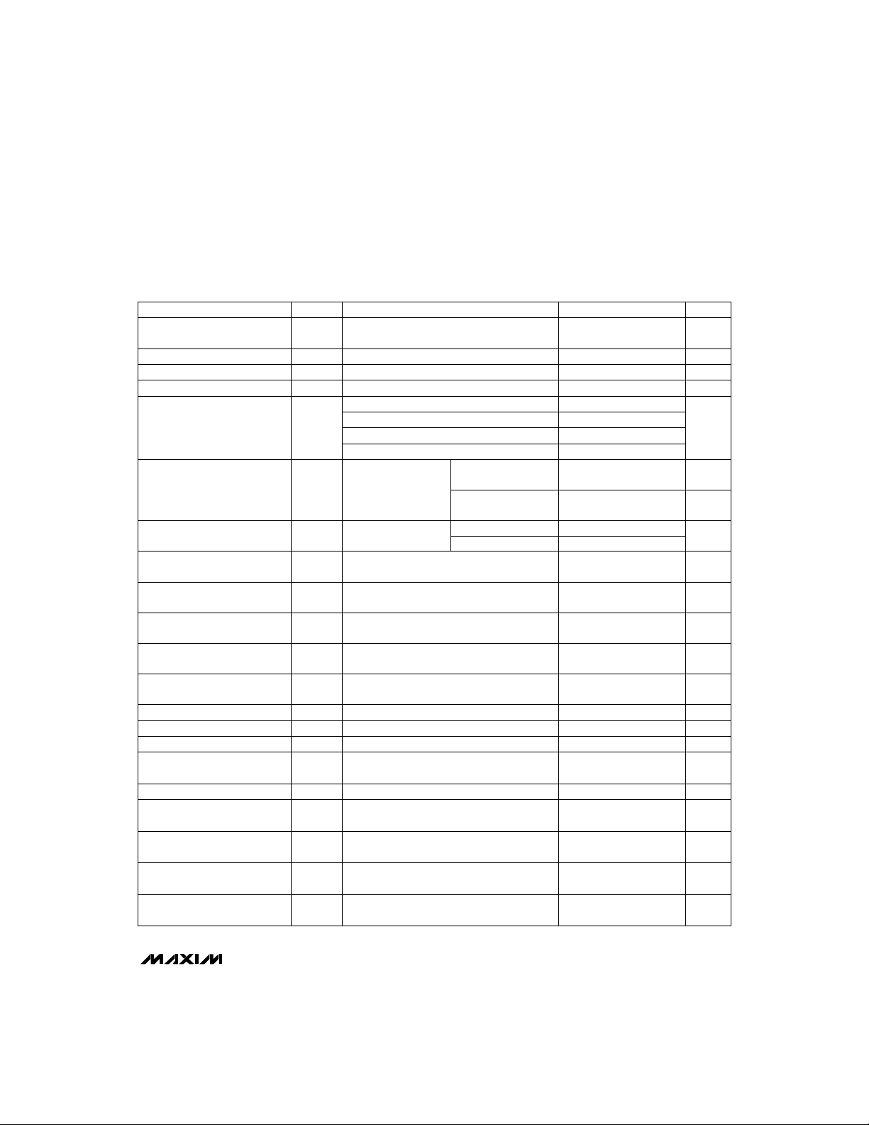
ELECTRICAL CHARACTERISTICS (continued)
(Circuit of Figure 1, VDD= +3.3V, V
BATT
= +16.8V, V
DCIN
= +18V, TA= 0°C to +85°C, unless otherwise noted. Typical values are at
T
A
= +25°C.)
V
CCV
= V
CCI
= V
CCS
= 0.25V to 2V
PDL to GND
From CSSP/CSSN to CCS, V
CLS
= 2.048V,
V
CSSP
- V
CSSN
= 102.4mV
From BATT to CCV
V
CSSN
- V
PDL
= 1V
V
CSSP
= V
CSSN
= 28V, V
DCIN
= 0
V
CVS
referred to V
BATT
V
CSSP
= V
CSSN
= V
DCIN
= 0 to 28V
Total of I
BATT
, I
CSIP,
and I
CSIN
;
V
BATT
= 0 to 20V, V
DCIN
= 0
Total of I
BATT
, I
CSIP,
and I
CSIN
;
V
BATT
= 0 to 20V, charge inhibited
R
CSS
= 40mΩ
Total of I
BATT
, I
CSIP,
and I
CSIN
;
V
BATT
= 0 to 20V
R
CS
= 50mΩ
Charging Voltage() = 0x1060
V
CVS
= 28V
ChargingVoltage() = 0x41A0
ChargingVoltage() = 0x3130
V
BATT
= 1V, R
CSI
= 50mΩ
ChargingVoltage() = 0x20D0
CONDITIONS
From CSIP/SCIN to CCI, ChargingCurrent() =
0x0BC0, V
CSIP
- V
CSIN
= 150.4mV
From BATT to CCV, ChargingVoltage() =
0x41A0, V
BATT
= 16.8V
V
CLS
= V
REF
/2 to V
REF
mV
150 300 600
CCV/CCI/CCS Clamp Voltage
(Note 4)
µA/mV
V/V
200 500
Battery Voltage-Error Amp DC
Gain
µA
-1 1
CSSP/CSSN Quiescent Current
µA-100 540 1000CSSP Input Bias Current
µA
-5 5
Total BATT Standby Current
µA
-100 100
Total BATT Quiescent Current
µA
-700 700
Total BATT Input Bias Current
V
020
BATT/CSIP/CSIN Input Voltage
Range
mA
20 128 200
BATT Undervoltage Charge
Current
2.282 2.56 2.838
kΩ
50 100 150
PDL Turn-On Resistance
mA
612
mV
100 200 300
V
PDL-HYS
PDL Load Switch Threshold
Hysteresis
PDL Turn-Off Current
A
4.714 5.12 5.526
mA
61.6 128 194.4
A
2.798 3.008 3.218
I0BATT Charge Current (Note 3)
4.150 4.192 4.234
µA
620
CVS Input Bias Current
16.666 16.8 16.934
V0BATT Full-Charge Voltage V
12.492 12.592 12.692
8.333 8.4 8.467
UNITSMIN TYP MAXSYMBOLPARAMETER
0.5 1 2
Input Current-Error Amp
Transconductance
µA/mV
0.5 1 2
Battery Current-Error Amp
Transconductance
µA/mV
0.111 0.222 0.444
Battery Voltage-Error Amp
Transconductance
µA
-1 0.05 1
CLS Input Bias Current
DCIN Source Current Limit
(Note 3)
ChargingCurrent() =
0x0BC0
ChargingCurrent() =
0x0080
V
CLS
= 4.096V
V
CLS
= 2.048V
V
CSSP
= C
CSSN
= V
DCIN
= 0 to 28V mA-100 35 100CSSN Input Bias Current
MAX1645
Advanced Chemistry-Independent, Level 2
Battery Charger with Input Current Limiting
4 _______________________________________________________________________________________
V
SDA
= 0.4V
All 4 comparators, VDD= 2.8V to 5.65V
VDD= 2.8V to 5.65V, V
THM
falling
VDD= 2.8V to 5.65V, V
THM
falling
DLO high or low, V
DLOV
= 4.5V
DHI high or low, V
BST
- VLX= 4.5V
VDD= 2.8V to 5.65V, V
THM
falling
VDD= 2.8V to 5.65V, V
THM
falling
R
CSI
= 50mΩ
V
DLOV
= V
LDO
, DLO low
V
DCIN
= 28V, V
BATT
= VLX= 20V
V
DCIN
= 0, V
BATT
= VLX= 20V
V
THM
= 4% of VDDto 96% of VDD,
V
DD
= 2.8V to 5.65V
DHI high
CONDITIONS
mA
6
SDA Output Low Sink Current
µA
-1 1
SDA/SCL Input Bias Current
mV
220
SDA/SCL Input Hysteresis
V
1.4
SDA/SCL Input High Voltage
V
0.6
SDA/SCL Input Low Voltage
1
Thermistor Comparator
Threshold Hysteresis
6 7.5 9
Thermistor Underrange
Threshold
% of V
DD
22 23.5 25
Thermistor Hot Threshold
74 75.5 77
Thermistor Cold Threshold
89.5 91 92.5
Thermistor Overrange Threshold
µA-1 1THM Input Bias Current
ms
51015
t
ON
Maximum On-Time
µs
1 1.25 1.5
t
OFF
Minimum Off-Time
Ω
614
DLO Output Resistance
Ω
6 14
DHI Output Resistance
A
5.0 6.0 7.0
Inductor Peak Current Limit
µA
5 10
DLOV Supply Current
%
99 99.99
Maximum Duty Cycle
µA
200 500
LX Input Bias Current
µA
1
LX Input Quiescent Current
µA
615
BST Supply Current
UNITSMIN TYP MAXSYMBOLPARAMETER
I
INT
= 1mA
V
INT
= 5.65V
mV
25 200
µA
1
INT Output High Leakage
INT Output Low Voltage
ns
0
t
HD:DAT
SDA Hold Time from SCL
ns
250
t
SU:DAT
SDA Setup Time from SCL
µs
4
t
HIGH
SCL High Period
µs
4.7
t
LOW
SCL Low Period
µs
4.7
t
SU:STA
Start Condition Setup Time
from SCL
µs
4
t
HD:STA
Start Condition Hold Time
from SCL
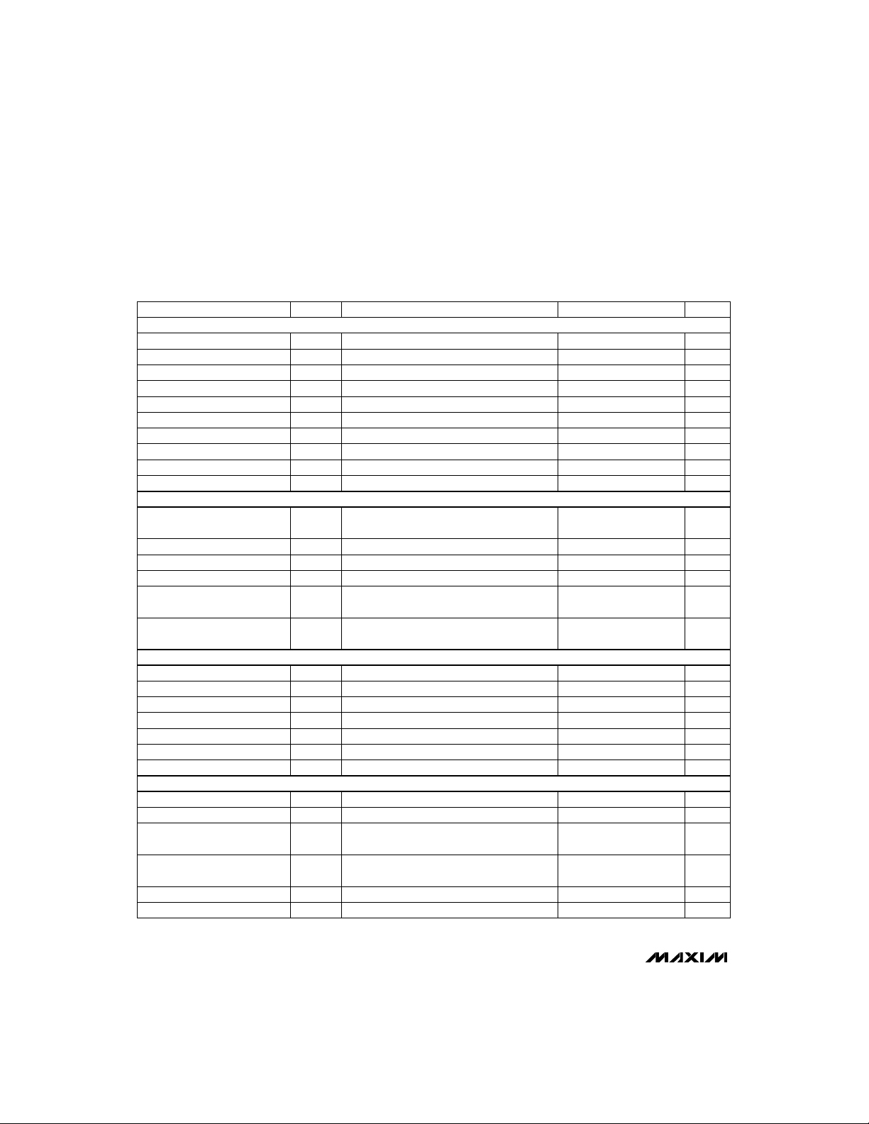
ELECTRICAL CHARACTERISTICS (continued)
(Circuit of Figure 1, VDD= +3.3V, V
BATT
= +16.8V, V
DCIN
= +18V, TA= 0°C to +85°C, unless otherwise noted. Typical values are at
T
A
= +25°C.)
% of V
DD
% of V
DD
% of V
DD
% of V
DD
DC-TO-DC CONVERTER SPECIFICATIONS
THERMISTOR COMPARATOR SPECIFICATIONS
SMB INTERFACE LEVEL SPECIFICATIONS (VDD= 2.8V to 5.65V)
SMB INTERFACE TIMING SPECIFICATIONS (VDD= 2.8V to 5.65V, Figures 4 and 5)
MAX1645
Advanced Chemistry-Independent, Level 2
Battery Charger with Input Current Limiting
_______________________________________________________________________________________ 5
ELECTRICAL CHARACTERISTICS (continued)
(Circuit of Figure 1, VDD= +3.3V, V
BATT
= +16.8V, V
DCIN
= +18V, TA= 0°C to +85°C, unless otherwise noted. Typical values are at
T
A
= +25°C.)
CONDITIONS UNITSMIN TYP MAXSYMBOLPARAMETER
sec
140 175 210
t
WDT
Maximum Charge Period
Without a ChargingVoltage() or
Charging Current() Loaded
µs
1
t
DV
SDA Output Data Valid from SCL
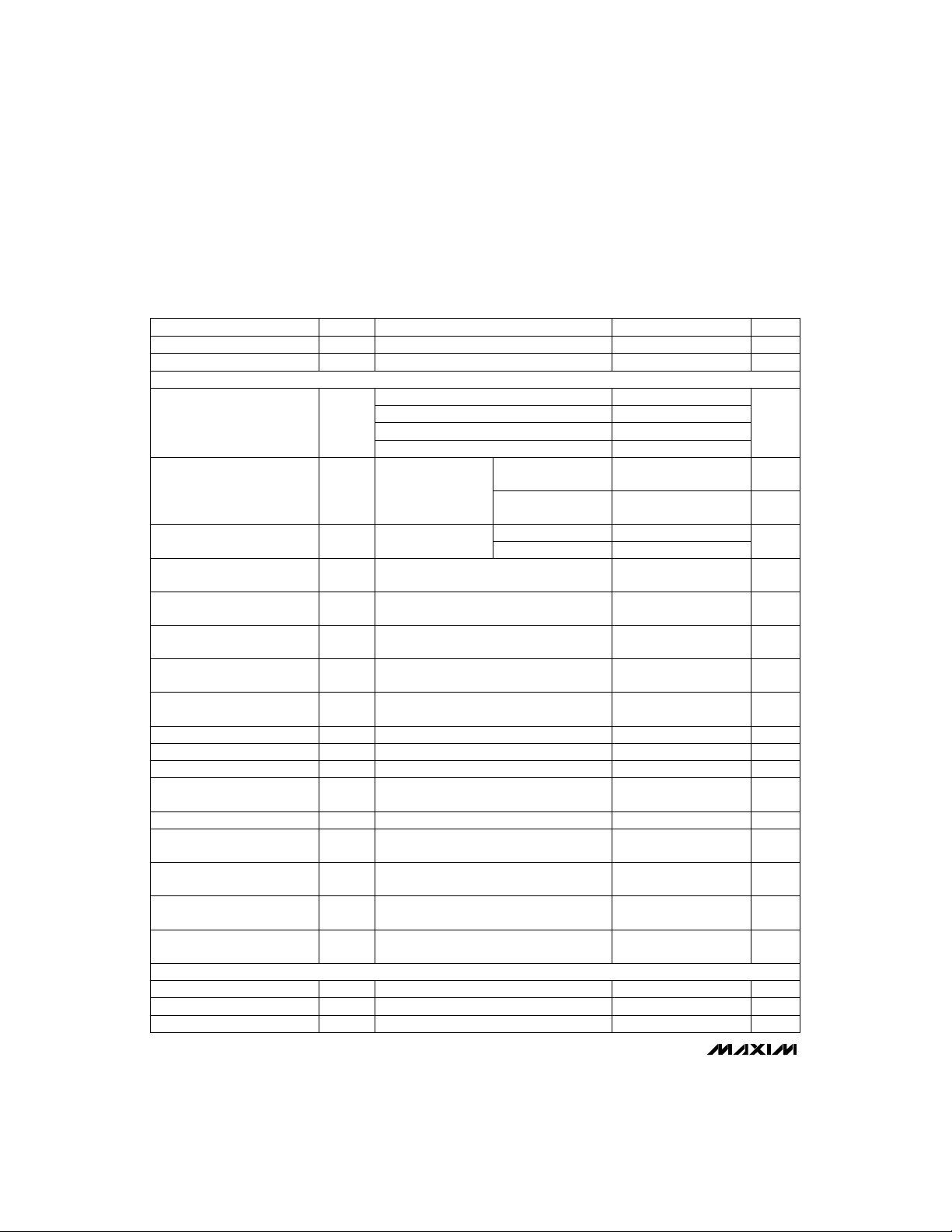
ELECTRICAL CHARACTERISTICS
(Circuit of Figure 1, VDD= +3.3V, V
BATT
= +16.8V, V
DCIN
= +18V, TA= -40°C to +85°C, unless otherwise noted. Guaranteed by design.)
PARAMETER SYMBOL MIN MAX UNITS
LDO Output Voltage V
LDO
5.15 5.65
V
7
DCIN Undervoltage Threshold
7.85
V
DCIN Supply Current Charging
Inhibited
2
mA
VDDInput Voltage Range
(Note 1)
2.8 5.65
V
VDDUndervoltage Threshold
2.8
V
2.1
VDDQuiescent Current I
DD
150
µA
DCIN Typical Operating Range V
DCIN
828
V
DCIN Supply Current I
DCIN
6
mA
REF Output Voltage V
REF
4.035 4.157
V
BATT Undervoltage Threshold
(Note 2)
2.4 2.8
V
PDS Charging Source Switch
Turn-Off Threshold
V
PDS-OFF
50 150
mV
PDS Charging Source Switch
Threshold Hysteresis
V
PDS-HYS
100 300
mV
PDS Output Low Voltage, PDS
Below CSSP
812
V
PDS Turn-On Current
100 300
µA
PDS Turn-Off Current
10
mA
PDL Load Switch Turn-Off
Threshold
V
PDL-OFF
-150 -50
mV
PDL Load Switch Threshold
Hysteresis
V
PDL-HYS
100 300
mV
PDL Turn-Off Current
6
mA
CONDITIONS
0 < I
REF
< 200µA
8V < V
DCIN
< 28V, 0 < I
LDO
< 15mA
When I
CHARGE
drops to 128mA
When AC_PRESENT
switches
8V < V
DCIN
< 28V
8V < V
DCIN
< 28V
When the SMB responds to commands
V
CVS
referred to V
BATT
, V
CVS
falling
V
CVS
referred to V
BATT
0 < V
DCIN
< 6V, VDD= 5V, V
SCL
= 5V,
V
SDA
= 5V
I
PDS
= 0
PDS = CSSP
V
PDS
= V
CSSP
- 2V, V
DCIN
= 16V
V
CVS
referred to V
BATT
, V
CVS
rising
V
CVS
referred to V
BATT
V
CSSN
- V
PDL
= 1V
8V < V
DCIN
< 28V
DCIN rising
DCIN falling
VDDrising
VDDfalling
GENERAL SPECIFICATIONS
MAX1645
Advanced Chemistry-Independent, Level 2
Battery Charger with Input Current Limiting
6 _______________________________________________________________________________________
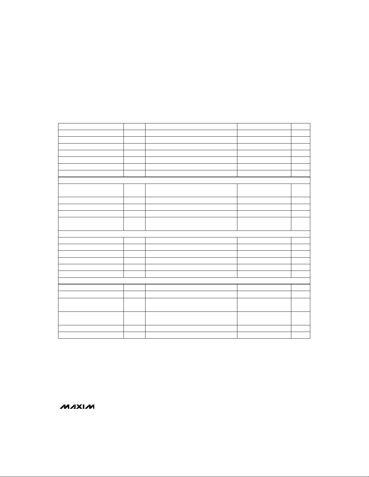
ELECTRICAL CHARACTERISTICS (continued)
(Circuit of Figure 1, VDD= +3.3V, V
BATT
= +16.8V, V
DCIN
= +18V, TA= -40°C to +85°C, unless otherwise noted. Guaranteed by design.)
Maximum Duty Cycle
99
%
Minimum Off-Time t
OFF
1 1.5
µs
Maximum On-Time t
ON
515
ms
PARAMETER SYMBOL MIN MAX UNITS
4.124 4.260
8.266 8.534
12.391 12.793
BATT Full-Charge Voltage V0
16.532 17.068
V
BATT Charge Current (Note 3) I0
2.608 3.408
A
15.2 240.8
mA
DCIN Source Current Limit
(Note 3)
4.358 5.882
A
2.054 3.006
CVS Input Bias Current
PDL Turn-On Resistance
50 150
kΩ
20
µA
BATT Undervoltage Charge
Current
20 200
mA
BATT/CSIP/CSIN Input Voltage
Range
020
V
Total BATT Input Bias Current
-700 700
µA
Total BATT Quiescent Current
-100 100
µA
Total BATT Standby Current
-5 5
µA
CSSP/Input Bias Current
-100 1000
µA
CSSP/CSSN Quiescent Current
-1 1
µA
Battery Voltage-Error Amp DC
Gain
200
V/V
CLS Input Bias Current
-1 1
µA
Battery Voltage-Error Amp
Transconductance
0.111 0.444
µA/mV
Battery Current-Error Amp
Transconductance
0.5 2
µA/mV
Input Current-Error Amp
Transconductance
0.5 2
µA/mV
CCV/CCI/CCS Clamp Voltage
(Note 4)
150 600
mV
CONDITIONS
V
BATT
= 1V, R
CSI
= 50mΩ
ChargingVoltage() = 0x1060
ChargingVoltage() = 0x20D0
ChargingVoltage() = 0x3130
ChargingVoltage() = 0x41A0
R
CSI
= 50mΩ
Total of I
BATT
, I
CSIP,
and I
CSIN
;
V
BATT
= 0 to 20V
Total of I
BATT
, I
CSIP,
and I
CSIN
;
V
BATT
= 0 to 20V, charge inhibited
R
CSS
= 40mΩ
Total of I
BATT
, I
CSIP,
and I
CSIN
;
V
BATT
= 0 to 20V, V
DCIN
= 0
V
CSSP
= V
CSSN
= V
DCIN
= 28V
V
CSSP
= V
CSSN
= 28V, V
DCIN
= 0
PDL to GND
From BATT to CCV
V
CVS
= 28V
V
CLS
= V
REF
/2 to V
REF
From BATT to CCV, ChargingVoltage() =
0x41A0, V
BATT
= 16.8V
From CSIP/CSIN to CCI, ChargingCurrent() =
0x0BC0, V
CSIP-VCSIN
= 150.4mV
From CSSP/CSSN to CCS, V
CLS
= 2.048V,
V
CSSP
- V
CSSN
= 102.4mV
V
CCV
= V
CCI
= V
CCS
= 0.25V to 2V
ChargingCurrent() =
0x0BC0
ChargingCurrent() =
0x0080
V
CLS
= 4.096V
V
CLS
= 2.048V
CSSN Input Bias Current
-100 100
µAV
CSSP
= V
CSSN
= V
DCIN
= 28V
DC-TO-DC CONVERTER SPECIFICATIONS
ERROR AMPLIFIER SPECIFICATIONS
MAX1645
Advanced Chemistry-Independent, Level 2
Battery Charger with Input Current Limiting
_______________________________________________________________________________________ 7
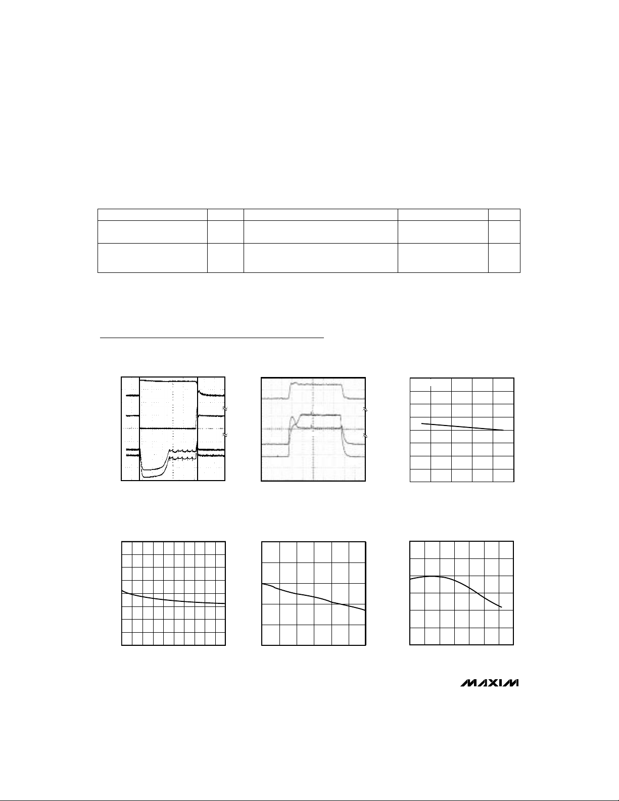
ELECTRICAL CHARACTERISTICS (continued)
(Circuit of Figure 1, VDD= +3.3V, V
BATT
= +16.8V, V
DCIN
= +18V, TA= -40°C to +85°C, unless otherwise noted. Guaranteed by design.)
SDA Hold Time from SCL t
HD:DAT
0
ns
Start Condition Hold Time
from SCL
Start Condition Setup Time
from SCL
t
SU:STA
4.7
µs
t
HD:STA
4
µs
SDA Setup Time from SCL t
SU:DAT
250
ns
PARAMETER SYMBOL MIN MAX UNITS
DLO Output Resistance
14
Ω
DHI Output Resistance
14
Ω
Inductor Peak Current Limit
5.0 7.0
A
DLOV Supply Current
10
µA
THM Input Bias Current
-1 1
µA
Thermistor Overrange Threshold
89.5 92.5
Thermistor Cold Threshold
74 77
LX Input Quiescent Current
LX Input Bias Current
500
µA
1
µA
BST Supply Current
15
µA
Thermistor Hot Threshold
22 25
% of V
DD
Thermistor Underrange
Threshold
69
SDA/SCL Input Low Voltage
0.6
V
SDA/SCL Input High Voltage
1.4
V
SDA/SCL Input Bias Current
-1 1
µA
SDA Output Low Sink Current
6
mA
INT Output High Leakage
1
µA
INT Output Low Voltage
200
mV
SCL High Period t
HIGH
4
µs
SCL Low Period t
LOW
4.7
µs
CONDITIONS
VDD= 2.8V to 5.65V, V
THM
falling
DLO high or low, V
DLOV
= 4.5V
VDD= 2.8V to 5.65V, V
THM
falling
DHI high or low, V
BST
- VLX= 4.5V
R
CSI
= 50mΩ
V
DLOV
= V
LDO
, DLO low
V
THM
= 4% of VDDto 96% of VDD,
VDD= 2.8V to 5.65V
VDD= 2.8V to 5.65V, V
THM
falling
VDD= 2.8V to 5.65V, V
THM
falling
V
DCIN
= 28V, V
BATT
= VLX= 20V
V
SDA
= 0.4V
V
DCIN
= 0, V
BATT
= VLX= 20V
V
INT
= 5.65V
I
INT
= 1mA
DHI high
% of V
DD
% of V
DD
% of V
DD
SMB INTERFACE LEVEL SPECIFICATIONS (VDD= 2.8V to 5.65V)
THERMISTOR COMPARATOR SPECIFICATIONS
SMB INTERFACE TIMING SPECIFICATIONS (VDD= 2.8V to 5.65V, Figures 4 and 5)
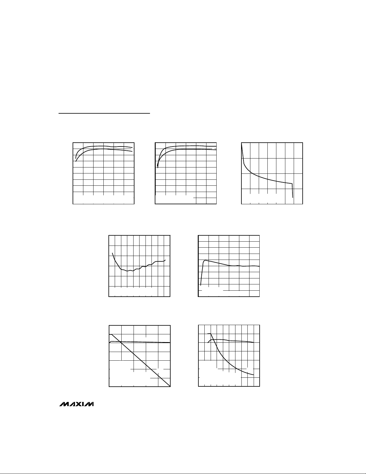
4.090
4.092
4.096
4.094
4.098
4.100
0 10050 150 200 250 300
REFERENCE VOLTAGE LOAD REGULATION
MAX1645 toc05
LOAD CURRENT (µA)
V
REF
(V)
5.20
5.30
5.25
5.35
5.50
5.55
5.45
5.40
5.60
0 468102 1214161820
LDO LOAD REGULATION
MAX1645 toc04
LOAD CURRENT (mA)
V
LDO
(V)
MAX1645
Advanced Chemistry-Independent, Level 2
Battery Charger with Input Current Limiting
8 _______________________________________________________________________________________
Typical Operating Characteristics
(Circuit of Figure 1, V
DCIN
= 20V, TA = +25°C, unless otherwise noted.)
LOAD-TRANSIENT RESPONSE
(BATTERY REMOVAL AND REINSERTION)
MAX1645 toc01
ChargingVoltage() = 15000mV
ChargingCurrent() = 1000mA
CCI
CCI
CCI
16V
14V
12V
1A
0
1.5V
V
CCV
/V
CCI
I
BATT
V
BATT
1V
0.5V
2ms/div
CCV
CCV
CCV
BATTERY REMOVED BATTERY INSERTED
LOAD-TRANSIENT RESPONSE
(STEP IN LOAD CURRENT)
MAX1645 toc02
ChargingCurrent() = 3008mA
V
BATT
= 16V
LOAD STEP: 0A TO 2A
I
SOURCE
LIMIT = 2.5A
CCS
CCS
CCS
4A
2A
0
2A
1V
0
1ms/div
CCI
CCI
CCI
V
CCV
/V
CCI
I
BATT
V
BATT
5.20
5.25
5.30
5.35
5.40
5.45
5.50
5.55
5.60
5 1015202530
LDO LINE REGULATION
MAX1645 toc03
V
DCIN
(V)
V
LDO
(V)
I
LOAD
= 0
4.080
4.090
4.085
4.100
4.095
4.105
4.110
-40 20 40-20 0 60 80 100
REFERENCE VOLTAGE
vs. TEMPERATURE
MAX1645 toc06
TEMPERATURE (°C)
V
REF
(V)
ELECTRICAL CHARACTERISTICS (continued)
(Circuit of Figure 1, VDD= +3.3V, V
BATT
= +16.8V, V
DCIN
= +18V, TA= -40°C to +85°C, unless otherwise noted. Guaranteed by design.)
Note 1: Guaranteed by meeting the SMB timing specs.
Note 2: The charger reverts to a trickle-charge mode of I
CHARGE
= 128mA below this threshold.
Note 3: Does not include current-sense resistor tolerance.
Note 4: Voltage difference between CCV, and CCI or CCS when one of these three pins is held low and the others try to pull high.
Maximum Charge Period
Without a ChargingVoltage() or
Charging Current() loaded
t
WDT
140 210
sec
SDA Output Data Valid
from SCL
t
DV
1
µs
PARAMETER SYMBOL MIN MAX UNITSCONDITIONS
MAX1645
Advanced Chemistry-Independent, Level 2
Battery Charger with Input Current Limiting
_______________________________________________________________________________________
9
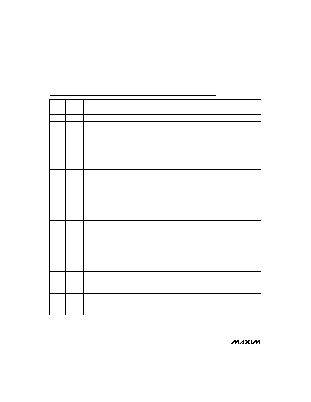
Typical Operating Characteristics (continued)
(Circuit of Figure 1, V
DCIN
= 20V, TA = +25°C, unless otherwise noted.)
EFFICIENCY vs. BATTERY CURRENT
(VOLTAGE-CONTROL LOOP)
100
95
90
85
80
75
70
EFFICIENCY (%)
65
60
A: V
= 20V, ChargingVoltage() = 16.8V
DCIN
55
= 16V, ChargingVoltage() = 8.4V
B: V
DCIN
50
0 1000500 1500 2000 2500 3000
BATTERY CURRENT (mA)
A
B
MAX1645 toc07
EFFICIENCY vs. BATTERY CURRENT
(CURRENT-CONTROL LOOP)
100
95
90
85
80
75
70
EFFICIENCY (%)
65
60
A: V
= 20V, V
DCIN
55
B: V
DCIN
50
0 1000500 1500 2000 2500 3000
= 16.8V
BATT
= 16V, V
= 8.4V
BATT
ChargingCurrent() (CODE)
A
B
0.001
MAX1645 toc08
0.01
0.1
1.0
DROP IN BATT OUTPUT VOLTAGE (%)
10
OUTPUT VI CHARACTERISTICS
ChargingVoltage() = 16,800mV
ChargingCurrent() = 3008mA
0 1500 2000500 1000 2500 3000 3500
LOAD CURRENT (mA)
MAX1645 toc09
BATT VOLTAGE ERROR
vs. ChargingVoltage() CODE
0.3
0.2
0.1
0
-0.1
BATT VOLTAGE ERROR (%)
-0.2
I
= 0
BATT
MEASURED AT AVAILABLE CODES
-0.3
0000 80004000 12000 16000 20000
ChargingVoltage() (CODE)
SOURCE/BATT CURRENT vs. LOAD CURRENT
WITH SOURCE CURRENT LIMIT
3.5
3.0
2.5
2.0
1.5
V
= 2V
CLS
= 40mΩ
R
CSS
1.0
V
SOURCE/BATT CURRENT (A)
= 16.8V
BATT
SOURCE CURRENT LIMIT = 2.5A
0.5
ChargingCurrent() = 3008mA
ChargingVoltage() = 18,432mV
0
0 1.00.5 1.5 2.0 2.5
I
IN
LOAD CURRENT (A)
I
BATT
MAX1645 toc10
MAX1645 toc12
CURRENT-SETTING ERROR
vs. ChargingCurrent() CODE
5
4
3
2
1
0
-1
-2
BATT CURRENT ERROR (%)
-3
V
= 12.6V
BATT
-4
MEASURED AT AVAILABLE CODES
-5
0 1000500 1500 2000 2500 3000
ChargingCurrent() (CODE)
SOURCE/BATT CURRENT vs. V
WITH SOURCE CURRENT LIMIT
3.5
3.0
2.5
2.0
1.5
I
= 2A
LOAD
= 2V
V
CLS
1.0
= 40mΩ
R
SOURCE/BATT CURRENT (A)
CSS
ChargingVoltage() = 18,432mV
0.5
ChargingCurrent() = 3008mA
SOURCE CURRENT LIMIT = 2.5A
0
042 6 8101214161820
I
IN
V
(V)
BATT
MAX1645 toc11
BATT
MAX1645 toc13
I
BATT
MAX1645
Advanced Chemistry-Independent, Level 2
Battery Charger with Input Current Limiting
10 ______________________________________________________________________________________
Pin Description
Battery Voltage OutputBATT9
DAC Voltage Output DAC10
Logic Circuitry Supply Voltage Input (2.8V to 5.65V) V
DD
11
Thermistor Voltage Input THM12
SMB Clock Input SCL13
Charging Source Compensation Capacitor Connection. Connect a 0.01µF capacitor from CCS to GND.CCS5
Battery Current-Loop Compensation Capacitor Connection. Connect a 0.01µF capacitor from CCI to GND. CCI6
Battery Voltage-Loop Compensation Capacitor Connection. Connect a 10kΩ resistor in series with a 0.01µF
capacitor to GND.
CCV7
Ground GND8
4.096V Reference Voltage OutputREF4
Source Current Limit InputCLS3
PIN
5.4V Linear-Regulator Voltage Output. Bypass with a 1µF capacitor to GND.LDO2
DC Supply Voltage InputDCIN1
FUNCTIONNAME
Inductor Voltage Sense InputLX22
High-Side NMOS Driver OutputDHI23
High-Side Driver Bootstrap Voltage Input. Bypass with 0.1µF capacitor to LX.BST24
Charging Source Current-Sense Negative InputCSSN25
Charging Source Current-Sense Positive InputCSSP26
Battery Current-Sense Positive InputCSIP18
Power GroundPGND19
Low-Side NMOS Driver OutputDLO20
Low-Side NMOS Driver Supply Voltage. Bypass with 0.1µF capacitor to GND.DLOV21
Battery Current-Sense Negative InputCSIN17
PMOS Load Switch Driver OutputPDL16
Interrupt Output. Open-drain output. Needs external pull-up.
INT
15
SMB Data Input/Output. Open-drain output. Needs external pull-up.SDA14
Charging Source PMOS Switch Driver OutputPDS27
Charging Source Voltage InputCVS28
 Loading...