_______________General Description
The MAX1640/MAX1641 CMOS, adjustable-output,
switch-mode current sources operate from a +5.5V to
+26V input, and are ideal for microprocessor-controlled
battery chargers. Charging current, maximum output
voltage, and pulse-trickle charge are programmed with
external resistors. Programming the off-time modifies
the switching frequency, suppressing undesirable harmonics in noise-sensitive circuits. The MAX1640’s highside current sensing allows the load to connect directly
to ground, eliminating ground-potential errors. The
MAX1641 incorporates a low-side current sense.
The MAX1640/MAX1641 step-down pulse-width-modulation (PWM) controllers use an external P-channel
MOSFET switch and an optional, external N-channel
MOSFET synchronous rectifier for increased efficiency.
An internal low-dropout linear regulator provides power
for the internal reference and circuitry as well as the
gate drive for the N-channel synchronous rectifier.
The MAX1640/MAX1641 are available in space-saving,
16-pin narrow QSOP packages.
________________________Applications
Battery-Powered Equipment
Laptop, Notebook, and Palmtop Computers
Handy Terminals
Portable Consumer Products
Cordless Phones
Cellular Phones
PCS Phones
Backup Battery Charger
____________________________Features
♦ 95% Efficiency
♦ +5.5V to +26V Input Supply Range
♦ 2V to 24V Adjustable-Output Voltage Range
♦ 100% Maximum Duty Cycle (Low Dropout)
♦ Up to 500kHz PWM Operation
♦ Optional Synchronous Rectifier
♦ 16-Pin QSOP Package
♦ Current-Sense Accuracy: 2% (MAX1641)
5.3% (MAX1640)
MAX1640/MAX1641
Adjustable-Output, Switch-Mode
Current Sources with Synchronous Rectifier
________________________________________________________________
Maxim Integrated Products
1
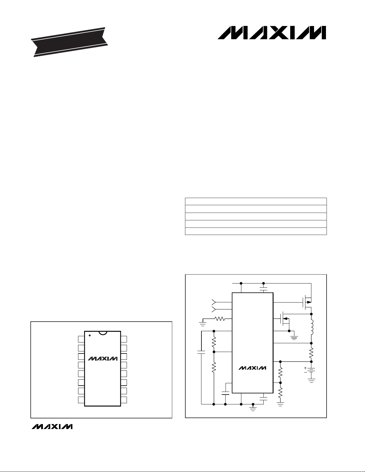
__________________Pin Configuration
16
15
14
13
12
11
10
9
1
2
3
4
5
6
7
8
LDOL IN
LDOH
PDRV
NDRV
PGND
CS+
CSGND
TOP VIEW
MAX1640
MAX1641
QSOP
TOFF
D1
REF
D0
CC
SET
TERM
19-1245; Rev 0; 7/97
PART
MAX1640C/D
MAX1640EEE
MAX1641C/D
0°C to +70°C
-40°C to +85°C
0°C to +70°C
TEMP. RANGE PIN-PACKAGE
Dice*
16 QSOP
Dice*
______________Ordering Information
*
Dice are specified at TA= +25°C, DC parameters only.
MAX1641EEE -40°C to +85°C 16 QSOP
IN LDOH
PDRV
NDRV
P
PGND
CS+
CS-
TERM
LDOLGND
OUT
D0
V
IN
= +5.5V TO +26V
D1
TOFF
R
TOFF
REF
SET
CC
MAX1640
__________Typical Operating Circuit
EVALUATION KIT
AVAILABLE
For free samples & the latest literature: http://www.maxim-ic.com, or phone 1-800-998-8800.
For small orders, phone 408-737-7600 ext. 3468.

MAX1640/MAX1641
Adjustable-Output, Switch-Mode
Current Source with Synchronous Rectifier
2 _______________________________________________________________________________________
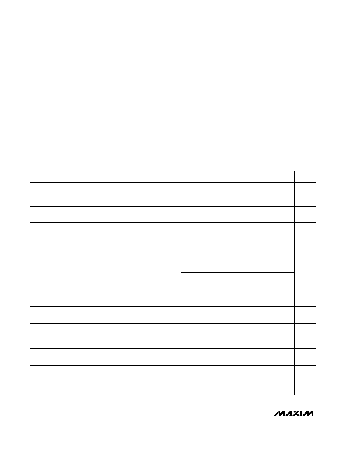
ABSOLUTE MAXIMUM RATINGS
ELECTRICAL CHARACTERISTICS
(VIN= +12V, V
OUT
= 6V, Circuit of Figure 2, TA= 0°C to +85°C, unless otherwise noted. Typical values are at TA= +25°C.)
Stresses beyond those listed under “Absolute Maximum Ratings” may cause permanent damage to the device. These are stress ratings only, and functional
operation of the device at these or any other conditions beyond those indicated in the operational sections of the specifications is not implied. Exposure to
absolute maximum rating conditions for extended periods may affect device reliability.
Note 1: This ratio is generated by a 1:8 clock divider and is not an error source for current calculations.
IN to GND...............................................................-0.3V to +28V
LDOH to IN...............................................................+0.3V to -6V
LDOL to GND...........................................................-0.3V to +6V
PDRV to GND .............................. (V
LDOH
- 0.3V) to (VIN+ 0.3V)
NDRV to GND.........................................-0.3V to (V
LDOL
+ 0.3V)
TOFF, REF, SET, TERM, CC to GND ......-0.3V to (V
LDOL
+ 0.3V)
D0, D1 to GND .........................................................-0.3V to +6V
CS+, CS- to GND ...................................................-0.3V to +28V
PGND to GND.....................................................................±0.3V
Continuous Power Dissipation (TA = +70°C)
QSOP (derate 8.30mW/°C above +70°C)................... 667mW
Operating Temperature Range
MAX164_EEE...................................................-40°C to +85°C
Storage Temperature Range.............................-65°C to +150°C
Lead Temperature (soldering, 10sec)............................ +300°C
I
REF
= 0 to 50µA
D0 = D1 = low
D0 = D1 = low (off mode)
D0 or D1 = high
V
OUT
= 2V to 24V
VIN= V
OUT
+ 0.5V to 26V
MAX1641
MAX1641
MAX1640
VIN= 5.5V to 26V, I
LOAD
= 0 to 20mA
VIN= 5.5V to 26V, I
LOAD
= 0 to 20mA
MAX1640
CONDITIONS
µA1V
SET
Input Current
mV4 10Reference Load Regulation
V1.96 2.00 2.04V
REF
Reference Voltage
V4.05 4.20 4.35V
LDOL
Undervoltage Lockout
µA1Output Current in Off Mode
500
mA2 4
Quiescent VINSupply Current
0.1
%/V
0.1 0.4
Output Current Compliance
%/V0.03Current-Sense Line Regulation
34 37.5 41
mV
36 42 48
147 150 153
mV
142 150 158
Full-Scale Current-Sense
Threshold
V
VIN- VIN- VIN-
5.5 5.0 4.5
V
LDOH
Linear-Regulator Output
Voltage, VINReferenced
V4.5 5.0 5.5V
LDOL
Linear-Regulator Output
Voltage, Ground Referenced
UNITSMIN TYP MAXSYMBOLPARAMETER
V5.5 26V
IN
Input Voltage Range
FET Drive Output Resistance PFET and NFET drive 12 Ω
Off-Time Range 1 10 µs
Off-Time Accuracy R
TOFF
= 62kΩ 1.7 2.2 2.7 µs
Pulse-Trickle Mode Duty-Cycle
Period
D0 = low, D1 = high, R
TOFF
= 100kΩ 27 33 40 ms
Pulse-Trickle Mode Duty Cycle
(Note 1)
D0 = low, D1 = high, R
TOFF
= 100kΩ 12.5 %
Quarter-Scale Current-Sense
Threshold
MAX1640
MAX1641
µA

MAX1640/MAX1641
Adjustable-Output, Switch-Mode
Current Source with Synchronous Rectifier
_______________________________________________________________________________________ 3
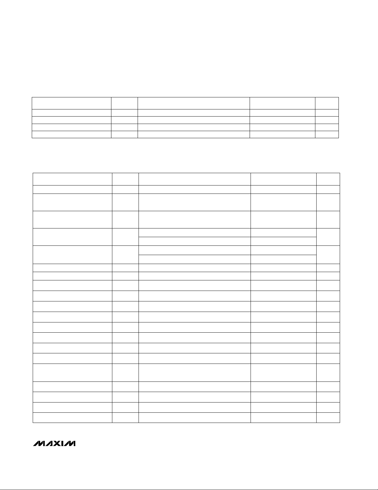
ELECTRICAL CHARACTERISTICS
(VIN= +12V, V
OUT
= 6V, Circuit of Figure 2, TA= -40°C to +85°C, unless otherwise noted.)
I
REF
= 0 to 50µA
V
OUT
= 2V to 24V (MAX1640)
D0 = D1 = low
D0 or D1 = high
FET Drive Output Resistance
MAX1641
MAX1640
VIN= 5.5V to 26V,
I
LOAD
= 0 to 20mA
VIN= 5.5V to 26V,
I
LOAD
= 0 to 20mA
MAX1640
CONDITIONS
µA1V
SET
Input Current
mV10Reference Load Regulation
V1.94 2.06V
REF
Reference Voltage
V4.0 4.4V
LDOL
Undervoltage Lockout
µA1Output Current in Off Mode
mA4Quiescent VINSupply Current
%/V0.4Output Current Compliance
mV
34 48
Quarter-Scale Current-Sense
Threshold
12 Ω
Off-Time Range
V5.5 26V
IN
Input Voltage Range
1.5 8 µs
Off-Time Accuracy R
TOFF
= 62kΩ 1.5 2.5 µs
146 154
Pulse-Trickle Mode Duty-Cycle
Period
mV
141 159
Full-Scale Current-Sense
Threshold
V
VIN- VIN-
5.5 4.5
V
LDOH
Linear-Regulator Output
Voltage, VINReferenced
D0 = low, D1 = high, R
TOFF
= 50kΩ 25 42 ms
V4.5 5.5V
LDOL
Linear-Regulator Output
Voltage, Ground Referenced
UNITSMIN TYP MAXSYMBOLPARAMETER
PWM Maximum Duty Cycle 100 %
Input Low Voltage V
IL
D0, D1 0.8 V
Input High Voltage V
IH
D0, D1 2.4 V
Input Leakage Current I
IN
D0, D1 ±1 µA
33 42MAX1641
ELECTRICAL CHARACTERISTICS (continued)
(VIN= +12V, V
OUT
= 6V, Circuit of Figure 2, TA= 0°C to +85°C, unless otherwise noted. Typical values are at TA= +25°C.)
CONDITIONS UNITSMIN TYP MAXSYMBOLPARAMETER
PWM Maximum Duty Cycle 100 %
Input Low Voltage V
IL
D0, D1 0.8 V
Input High Voltage V
IH
D0, D1 2.4 V
Input Leakage Current I
IN
D0, D1 ±1 µA

MAX1640/MAX1641
Adjustable-Output, Switch-Mode
Current Source with Synchronous Rectifier
4 _______________________________________________________________________________________
0.45
0.51
0.49
0.47
0.53
0.55
0.57
0.59
0.61
0.63
0.65
4 128 16 20 24 28
OFF-MODE SUPPLY CURRENT
(NO-LOAD)
MAX1640/41-TOC07
INPUT VOLTAGE (V)
OFF-MODE SUPPLY CURRENT (mA)
TA = -40°C
TA = +25°C
TA = +85°C
10,000
1
0 50 100 150 200 250 300 350 400
SWITCHING FREQUENCY vs. R
TOFF
MAX1640/41 TOC 08
T
OFF
(kΩ)
SWITCHING FREQUENCY (kHz)
10
100
1000
V
OUT
= +3V
V
OUT
= +6V
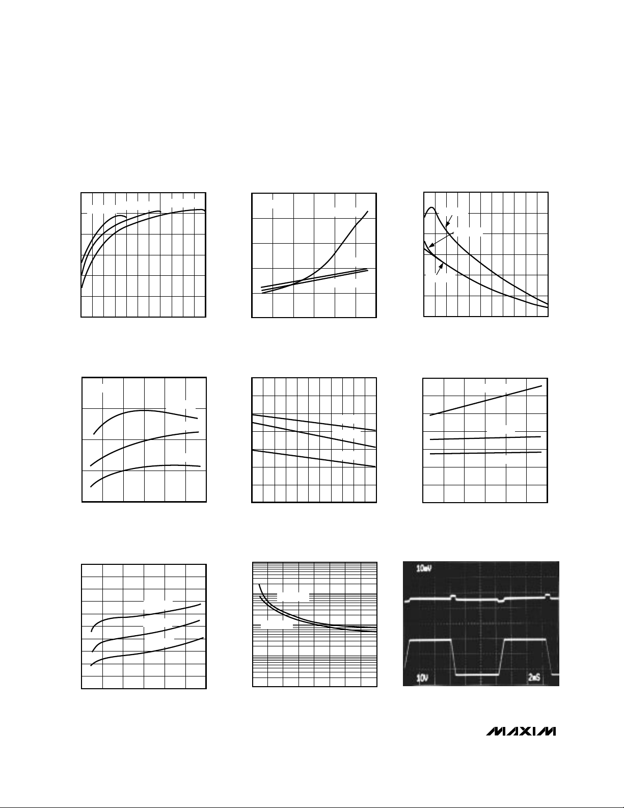
__________________________________________Typical Operating Characteristics
(Circuit of Figure 2, TA = +25°C, unless otherwise noted.)
40
60
50
80
70
90
100
2 6 8 104 12 14 16 18 20 22 24
EFFICIENCY vs. OUTPUT VOLTAGE
MAX1640/41-TOC01
OUTPUT VOLTAGE (V)
EFFICIENCY (%)
VIN = 12V
VIN = 18V
VIN = 26V
1.460
1.470
1.480
1.490
1.500
1.510
4 128 16 20 24 28
MAX1640
OUTPUT CURRENT vs. INPUT VOLTAGE
MAX1640/41 TOC02
INPUT VOLTAGE (V)
OUTPUT CURRENT (A)
TA = -40°C
(V
OUT
= 4V)
TA = +25°C
TA = +85°C
1.450
1.470
1.460
1.490
1.480
1.500
1.510
2 6 8 104 12 14 16 18 20 22 24
MAX1640
OUTPUT CURRENT vs. OUTPUT VOLTAGE
MAX1640/41-TOC03
OUTPUT VOLTAGE (V)
OUTPUT CURRENT (A)
TA = -40°C
TA = +85°C
TA = +25°C
1.450
1.475
1.500
1.525
1.550
4 128 16 20 24 28
MAX1641
OUTPUT CURRENT vs. INPUT VOLTAGE
MAX1640/41 TOC04
INPUT VOLTAGE (V)
OUTPUT CURRENT (A)
TA = -40°C
(V
OUT
= 4V)
TA = +25°C
TA = +85°C
1.420
1.460
1.440
1.500
1.480
1.540
1.520
1.560
2 6 8 104 12 14 16 18 20 22 24
MAX1641
OUTPUT CURRENT vs. OUTPUT VOLTAGE
MAX1640/41-TOC05
V
OUT
(V)
OUTPUT CURRENT (A)
TA = -40°C
TA = +25°C
TA = +85°C
1.5
1.9
1.7
2.1
2.3
2.5
2.7
2.9
4 128 16 20 24 28
QUIESCENT CURRENT
vs. INPUT VOLTAGE (NO-LOAD)
MAX1640/41-TOC06
INPUT VOLTAGE (V)
QUIESCENT CURRENT (mA)
TA = -40°C
TA = +25°C
TA = +85°C
A: OUTPUT CURRENT, D1 = D0 = 1 1A/div
V
LOAD
= 3V
B: INPUT VOLTAGE, 10V/div
LINE-TRANSIENT RESPONSE
A
B
0A
0V
2ms/div
MAX1640/41 TOC 09
 Loading...