_______________General Description
The MAX1636 is a synchronous, buck, switch-mode,
power-supply controller that generates the CPU supply
voltage in battery-powered systems. It achieves ±1%
output voltage accuracy and offers the excellent loadtransient response needed by upcoming generations of
dynamic-clock CPUs.
Up to 95% efficiency is achieved through synchronous
rectification and Maxim’s proprietary Idle Mode™ control scheme. Efficiency is greater than 80% over a
1000:1 load-current range, extending battery life in system-suspend or standby modes. Excellent dynamic
response corrects output load transients caused by the
latest dynamic-clock CPUs within five 300kHz clock
cycles. Strong, 1A, on-board gate drivers ensure fast,
external N-channel MOSFET switching.
The MAX1636 features a logic-controlled and synchronizable, fixed-frequency, pulse-width-modulation (PWM)
operating mode that reduces noise and RF interference
in sensitive mobile communications and pen-entry applications. Holding SKIP high forces fixed-frequency mode
for lowest noise under all load conditions.
For a low-cost version that omits the +5V VL linearregulator block and comes in a smaller 16-pin QSOP
package, refer to the MAX1637 data sheet.
________________________Applications
Notebook Computers
Subnotebook Computers
Desktop Computers
Bus-Termination Supplies
____________________________Features
♦ ±1% DC Accuracy (Adjustable Mode)
♦ Output Overvoltage Crowbar Protection
♦ Output Undervoltage Shutdown
♦ Adjustable Switching Frequency to 340kHz
♦ Low-Dropout Operation
♦ Idle Mode Pulse-Skipping Operation
♦ 1.10V to 5.5V Adjustable Output Voltage
♦ 2.5V/3.3V Dual-Mode Fixed-Output Settings
♦ Internal Digital Soft-Start
♦ 1.1V ±1% Reference Output
♦ 3µA (typ) Shutdown Current
♦ Open-Drain Power-Good Output (
RREESSEETT
)
♦ 20-Pin SSOP Package
MAX1636
Low-Voltage, Precision Step-Down
Controller for Portable CPU Power
________________________________________________________________
Maxim Integrated Products
1
20
19
18
17
16
15
14
13
1
2
3
4
5
6
7
8
SKIP
LX
DH
BSTSHDN
RESET
CSL
CSH
TOP VIEW
PGND
DL
VL
V+SYNC
REF
CC
OVP
12
11
9
10
V
CC
FBGND
GND
MAX1636
SSOP
19-1268; Rev 0; 8/97
EVALUATION KIT
AVAILABLE
For free samples & the latest literature: http://www.maxim-ic.com, or phone 1-800-998-8800
For small orders, phone 408-737-7600 ext. 3468.
Idle Mode is a trademark of Maxim Integrated Products.
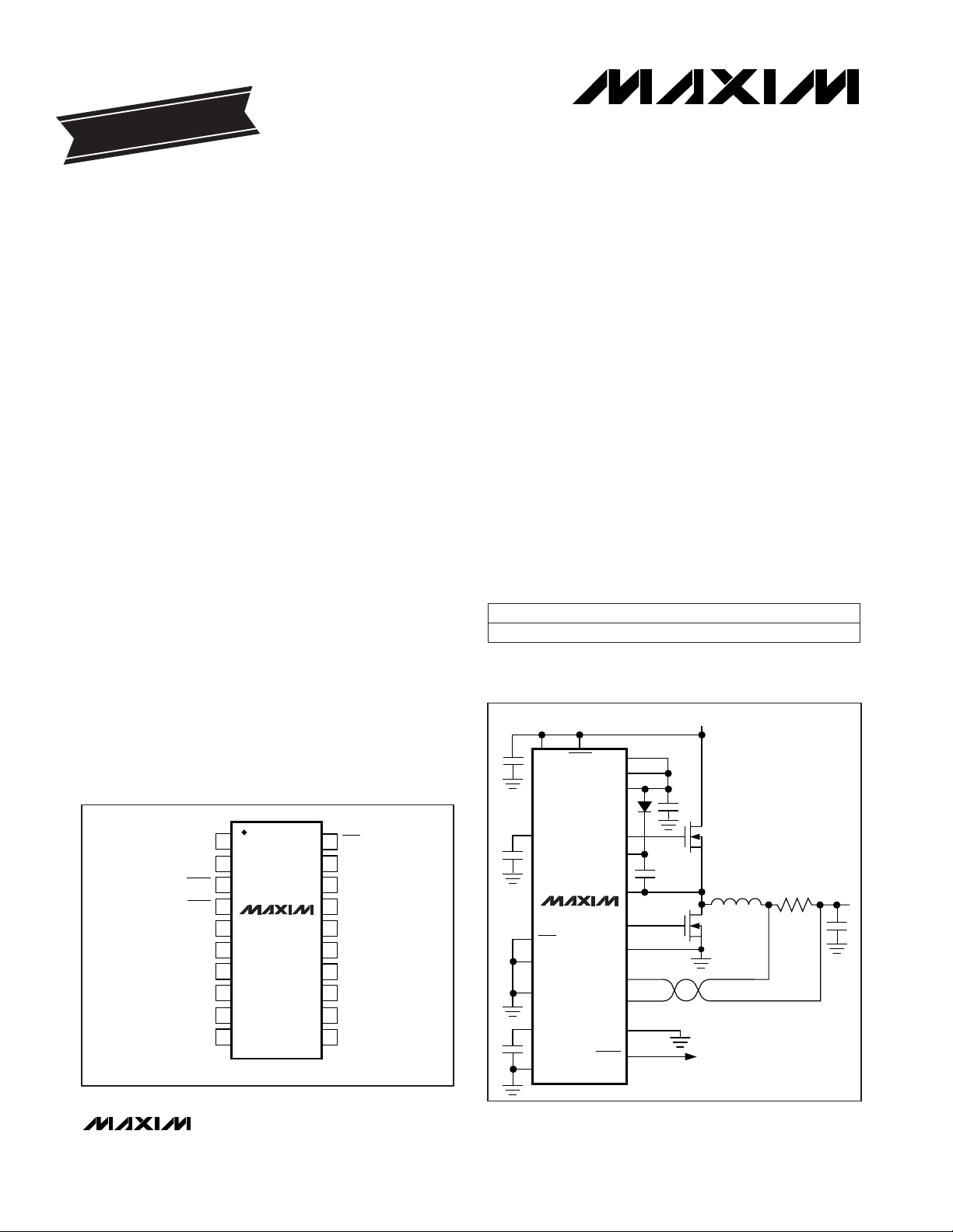
__________________Pin Configuration
__________Typical Operating Circuit
______________Ordering Information
MAX1636
V+ SHDN
GND
V
IN
DL
PGND
LX
DH
VL
V
CC
BST
OVP
CSH
CSL
FB
RESET
TO µP
CC
SKIP
GND
SYNC
REF
PART
MAX1636EAP -40°C to +85°C
TEMP. RANGE PIN-PACKAGE
20 SSOP

mV
MAX1636
Low-Voltage, Precision Step-Down
Controller for Portable CPU Power
2 _______________________________________________________________________________________
ABSOLUTE MAXIMUM RATINGS
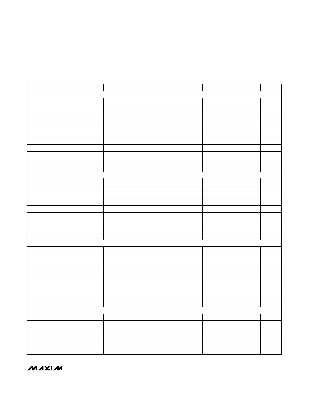
ELECTRICAL CHARACTERISTICS
(Circuit of Figure 1, V+ = 15V, SYNC = VL = VCC, IVL= 0mA, I
REF
= 0mA, TA= 0°C to +85°C, unless otherwise noted. Typical values
are at T
A
= +25°C.)
Stresses beyond those listed under “Absolute Maximum Ratings” may cause permanent damage to the device. These are stress ratings only, and functional
operation of the device at these or any other conditions beyond those indicated in the operational sections of the specifications is not implied. Exposure to
absolute maximum rating conditions for extended periods may affect device reliability.
V+ to GND ...............................................................-0.3V to 36V
GND to PGND........................................................................±2V
SHDN to GND.......................................................... -0.3V to 36V
LX, BST to GND....................................................... -0.3V to 36V
DH, BST to LX.............................................................-0.3V to 6V
VL, V
CC
, CSL, CSH, FB, SKIP to GND ...................... -0.3V to 6V
DL to GND.. ..................................................-0.3V to (VL + 0.3V)
REF, RESET, SYNC, CC, OVP to GND...... -0.3V to (V
CC
+ 0.3V)
VL Output Current...............................................................50mA
VL Short Circuit to GND..............................................Momentary
REF Output Current ............................................................20mA
REF Short Circuit to GND ....... ......................................Indefinite
Continuous Power Dissipation (TA= +70°C)
SSOP (derate 8.00mW/°C above +70°C) .....................640mW
Operating Temperature Range
MAX1636EAP. ..................................................-40°C to +85°C
Storage Temperature Range.............................-65°C to +160°C
Junction Temperature......................................................+150°C
Lead Temperature (soldering, 10sec).............................+300°C
Gate-driver supply rail
CSH - CSL
Input source for VL regulator
SHDN to full current limit, five levels
FB forced to REF
Positive direction
SHDN = GND, OVP = GND
VCC= 3.3V, output not switching
VCC= 3.3V, VL = 5V
VCC= VL = 5V
Internal chip supply rail
FB tied to V
OUT
, 0mV < (CSH - CSL) < 80mV, 4.5V
< V+ < 30V (includes line and load regulation)
FB tied to VCC, 0mV < (CSH - CSL) < 80mV, 4.5V
< V+ < 30V (includes line and load regulation)
VCC= 5V, output not switching
FB tied to GND, 0mV < (CSH - CSL) < 80mV, 4.5V
< V+ < 30V (includes line and load regulation)
Negative direction
CONDITIONS
mV20 30 40Idle Mode Switchover Threshold
clks512Soft-Start Ramp Time
nA-50 50FB Input Current
µA3 10Shutdown Supply Current (V+)
1.5
Power Consumption
2.0
-145 -100 -55
V4.2 5.5Input Voltage Range, VL
V4.5 30Input Voltage Range, V+
mV
80 100 120
Current-Limit Threshold
V
REF
3.6
V
V
REF
5.5
Output Adjustment Range
V3.15 5.5Input Voltage Range, V
CC
V1.090 1.100 1.110Output Voltage, Adj Mode
V2.486 2.55 2.614 Output Voltage, Fixed 2.5V Mode
V3.282 3.366 3.450Output Voltage, Fixed 3.3V Mode
UNITSMIN TYP MAXPARAMETER
mW
SMPS CONTROLLER
MAX1636
Low-Voltage, Precision Step-Down
Controller for Portable CPU Power
_______________________________________________________________________________________ 3
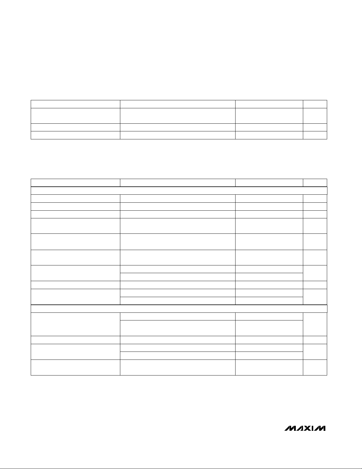
ELECTRICAL CHARACTERISTICS (continued)
(Circuit of Figure 1, V+ = 15V, SYNC = VL = VCC, IVL= 0mA, I
REF
= 0mA, TA= 0°C to +85°C, unless otherwise noted. Typical values
are at T
A
= +25°C.)
%
FB to DL delay, 22mV overdrive, C
GATE
= 2000pF
SHDN = GND, OVP = V
CC
FB, with respect to regulation point
VCC= 5V, I(VL) = 0, V+ = 4.5V
(includes PNP base current)
VCC= 5V, I(VL) = 0
Guaranteed by design
SYNC = V
CC
SYNC = GND
SYNC = V
CC
I(VL) = 0 to 25mA, 5V < V+ < 30V
I(VL) = 0 to 25mA, 6V < V+ < 30V
Rising edge, hysteresis = 25mV
SYNC = GND
REF load = 0 to 50µA
SYNC = GND
°C
150
µs
1.25
%
4 7 10
kHz
240 340
SYNC Input Frequency Range
ns
200
SYNC Input Rise/Fall Time
ns
200
SYNC Input Pulse Width Low
200
Maximum Duty Factor, Dropout Mode
98 99
93 96
µA
60
Standby Supply Current (V+)
µA
500
Regulator Supply Current (V+)
60
91 94
170 200 230
270 300 330
kHz
V
4.5 5.0 5.3
4.7 5.0 5.3
VL Output Voltage
V
3.15
VL/ VCCSwitchover Threshold
mV
10
REF Load Regulation
Hysteresis = 10°C
Rising edge, hysteresis = 25mV V
3.45 3.60 3.75
VL Undervoltage Lockout Threshold
No REF load V
1.090 1.100 1.110
REF Output Voltage
VCC= 3.3V to 5.5V mV
3
REF Line Regulation
Oscillator Frequency
%
nsSYNC Input Pulse Width High
Maximum Duty Factor
Overvoltage Trip Threshold
Thermal Shutdown Threshold
Overvoltage Fault Propagation Delay
%
Pin at GND or VCC; SKIP, OVP, SYNC
SHDN, SKIP, OVP, SYNC
SHDN, SKIP, OVP, SYNC
Falling edge (hysteresis = 1%)
From shutdown or power-on-reset state
% of nominal output
V
0.4
RESET Output Voltage Low
µA
-1 1
V
0.8
V
2.4
Logic Input Voltage High
clks
Catastrophic Output Undervoltage
Lockout Delay
Logic Input Voltage Low
Logic Input Bias Current
clks
32768
RESET Delay Time
%
-6 -3
RESET Trip Threshold
6144
Catastrophic Output Undervoltage
Lockout Threshold
60 70 80
I
SINK
= 4mA
+5.5V stress voltage applied µA
1
RESET Output Leakage Current
CONDITIONS UNITSMIN TYP MAXPARAMETER
SHDN = GND or V+
µA
-3 3
SHDN Input Bias Current
INTERNAL VL REGULATOR AND REFERENCE
OSCILLATOR
OVERVOLTAGE PROTECTION
INPUTS AND OUTPUTS
MAX1636
Low-Voltage, Precision Step-Down
Controller for Portable CPU Power
4 _______________________________________________________________________________________
Gate-driver supply rail
Input source for VL regulator
VCC= 3.3V, VL = 5V
VCC= VL = 5V
Internal chip supply rail
FB tied to V
OUT
, 0mV < (CSH - CSL) < 80mV, 4.5V
< V+ < 30V (includes line and load regulation)
FB tied to VCC, 0mV < (CSH - CSL) < 80mV, 4.5V
< V+ < 30V (includes line and load regulation)
FB tied to GND, 0mV < (CSH - CSL) < 80mV, 4.5V
< V+ < 30V (includes line and load regulation)
CONDITIONS
V4.2 5.5Input Voltage Range, VL
V4.5 30Input Voltage Range, V+
V
REF
3.6
V
V
REF
5.5
Output Adjustment Range
V3.15 5.5Input Voltage Range, V
CC
V1.086 1.114Output Voltage, Adj Mode
V2.432 2.635 Output Voltage, Fixed 2.5V Mode
V3.195 3.497Output Voltage, Fixed 3.3V Mode
UNITSMIN TYP MAXPARAMETER
High or low, DH or DL
DH or DL forced to 2V
CSH = CSL = 5V, V+ = VL = VCC=
GND, either CSH or CSL input
CONDITIONS
Ω7Gate-Driver On-Resistance
A1Gate-Driver Sink/Source Current
µA10
Current-Sense Input
Leakage Current
UNITSMIN TYP MAXPARAMETER
ELECTRICAL CHARACTERISTICS (continued)
(Circuit of Figure 1, V+ = 15V, SYNC = VL = VCC, IVL= 0mA, I
REF
= 0mA, TA= 0°C to +85°C, unless otherwise noted. Typical values
are at T
A
= +25°C.)
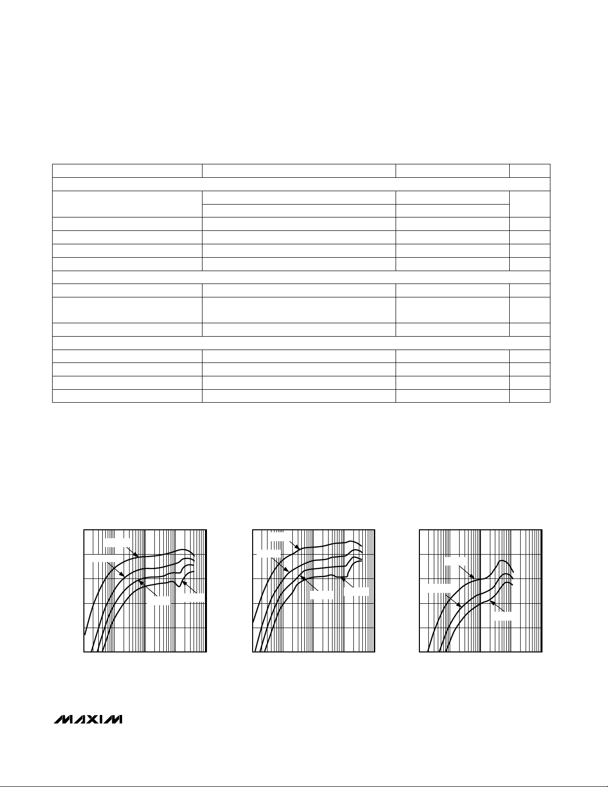
ELECTRICAL CHARACTERISTICS
(Circuit of Figure 1, V+ = 15V, SYNC = VL = VCC, IVL= 0mA, I
REF
= 0mA, TA=-40°C to +85°C, unless otherwise noted.) (Note 1)
VCC= 5V, I(VL) = 0
µA
60
Regulator Supply Current (V+)
VCC= 5V, I(VL) = 0, V+ = 4.5V
(includes PNP base current)
SHDN = GND, OVP = V
CC
µA60Standby Supply Current (V+)
I(VL) = 0 to 25mA, 6V < V+ < 30V
V
4.7 5.3
I(VL) = 0 to 25mA, 5V < V+ < 30V
VL Output Voltage
Rising edge, hysteresis = 25mV V3.45 3.91
4.5 5.3
VL Undervoltage Lockout
Threshold
500
VCC= 5V, output not switching
Positive direction
2.0
mV70 130Current-Limit Threshold
VCC= 3.3V, output not switching 1.5
Power Consumption mW
SMPS CONTROLLER
INTERNAL VL REGULATOR AND REFERENCE
MAX1636
Low-Voltage, Precision Step-Down
Controller for Portable CPU Power
_______________________________________________________________________________________ 5
ELECTRICAL CHARACTERISTICS (continued)
(Circuit of Figure 1, V+ = 15V, SYNC = VL = VCC, IVL= 0mA, I
REF
= 0mA, TA= -40°C to +85°C, unless otherwise noted.) (Note 1)
FB, with respect to regulation point
Guaranteed by design
SYNC = GND
SYNC = V
CC
%
3.5 10
Oscillator Frequency
nsSYNC Input Pulse Width High
Overvoltage Trip Threshold
kHz
240 340
SYNC Input Frequency Range
%
ns
200
SYNC Input Rise/Fall Time
ns
200
SYNC Input Pulse Width Low
SHDN, SKIP, OVP, SYNC
SHDN, SKIP, OVP, SYNC
200
Falling edge (hysteresis = 1%)
% of nominal output
V
0.4
RESET Output Voltage Low
V
0.8
V
170 230
2.4
270 330
Logic Input Voltage High
kHz
Logic Input Voltage Low
%
-7 -1.5
RESET Trip Threshold
Catastrophic Output Undervoltage
Lockout Threshold
60 80
I
SINK
= 4mA
High or low, DH or DL Ω
7
Gate-Driver On-Resistance
CONDITIONS UNITSMIN TYP MAXPARAMETER
OSCILLATOR
OVERVOLTAGE PROTECTION
INPUTS AND OUTPUTS
__________________________________________Typical Operating Characteristics
(Circuit of Figure 1, VIN= 7V, TA= +25°C, unless otherwise noted.)
100
50
1m 100m 110m 10
EFFICIENCY vs. LOAD CURRENT
(3.3V/3A CIRCUIT)
60
MAX1636 TOC01
LOAD CURRENT (A)
EFFICIENCY (%)
70
80
90
VIN = 22V
VIN = 30V
VIN = 7V
VIN = 15V
100
50
1m 100m 110m 10
EFFICIENCY vs. LOAD CURRENT
(5V/3A CIRCUIT)
60
MAX1636 TOC02
LOAD CURRENT (A)
EFFICIENCY (%)
70
80
90
VIN = 22V
VIN = 7V
VIN = 15V
VIN = 30V
100
50
1m 100m 110m 10
EFFICIENCY vs. LOAD CURRENT
(1.8V/1A CIRCUIT)
60
MAX1636 TOC03
LOAD CURRENT (A)
EFFICIENCY (%)
70
80
90
VIN = 15V
VIN = 7V
VIN = 22V
Note 1: Specifications to -40°C are guaranteed by design and not production tested.
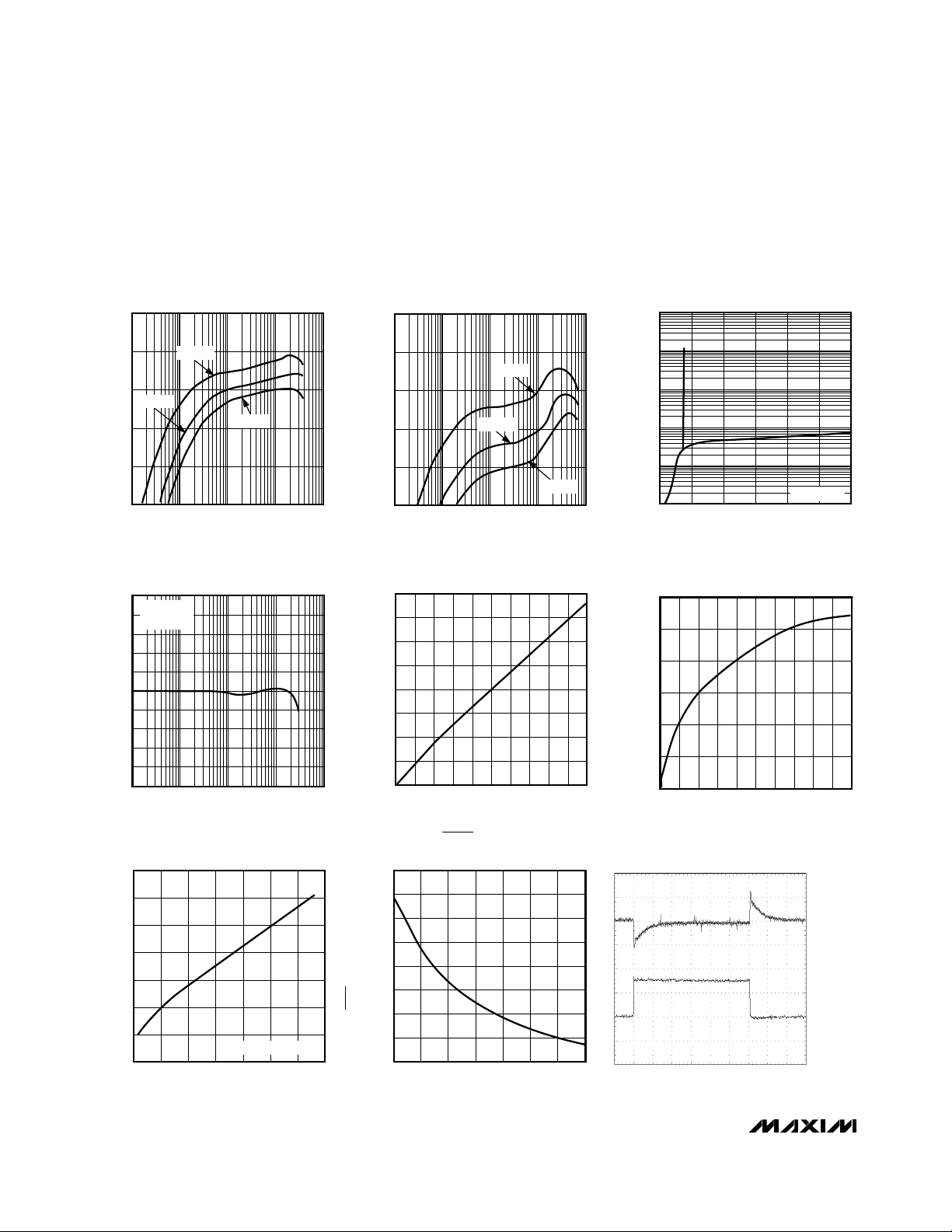
50
100
75
150
125
225
200
175
250
150 250200 300 350 400 450 500
MAX1636 TOC11
F
OSC
(kHz)
RESET TIME DELAY (ms)
RESET TIME DELAY
vs. OSC FREQUENCY
V
OUT
50mV/div
LOAD
CURRENT
0A
2A
4A
LOAD-TRANSIENT RESPONSE
(3.3V/3A, PWM MODE)
MAX1636 TOC12
100µs/div)
50
150
100
250
200
350
300
400
0 1.0 1.50.5 2.0 2.5 3.0 3.5
DROPOUT VOLTAGE
vs. LOAD CURRENT
MAX1636 TOC10
LOAD CURRENT (A)
V
IN
- V
OUT
(mV)
V
OUT
FORCED TO 4.95V
MAX1636
Low-Voltage, Precision Step-Down
Controller for Portable CPU Power
6 _______________________________________________________________________________________
5
-5
1m 100m 110m 10
-3
MAX1636 TOC07
LOAD CURRENT (A)
LOAD REGULATION ∆ V
OUT
(mV)
-1
1
3
-4
-2
0
2
4
LOAD REGULATION
vs. LOAD CURRENT
PWM MODE
V
OUT
= 5V
_____________________________Typical Operating Characteristics (continued)
(Circuit of Figure 1, VIN= 7V, TA = +25°C, unless otherwise noted.)
100
50
1m 100m 110m 10
EFFICIENCY vs. LOAD CURRENT
(1.8V/4A CIRCUIT)
60
MAX1636 TOC04
LOAD CURRENT (A)
EFFICIENCY (%)
70
80
90
VIN = 7V
VIN = 22V
VIN = 15V
100
50
1m 100m 110m 10
EFFICIENCY vs. LOAD CURRENT
(1.8V/7A CIRCUIT)
60
MAX1636 TOC05
LOAD CURRENT (A)
EFFICIENCY (%)
70
80
90
VIN = 15V
VIN = 7V
VIN = 22V
1000
0.01
0 15 20 25105 30
QUIESCENT SUPPLY CURRENT
vs. INPUT VOLTAGE
0.10
MAX1636 TOC06
INPUT VOLTAGE (V)
QUIESCENT SUPPLY CURRENT (mA)
1
10
100
V
OUT
= 3.3V
0
10
5
15
30
35
25
20
40
0 10 15 20 255 30 35 40 45 50
VL LOAD-REGULATION ERROR
vs. VL LOAD CURRENT
MAX1636 TOC08
VL LOAD CURRENT (mA)
LOAD REGULATION ∆V (mV)
0
0.3
0.2
0.1
0.4
0.5
0.6
0 403010 20 50 60 70 80 90 100
REF LOAD-REGULATION ERROR
vs. REF LOAD CURRENT
MAX1636 TOC09
REF LOAD CURRENT (µA)
LOAD REGULATION ∆V (mV)
MAX1636
Low-Voltage, Precision Step-Down
Controller for Portable CPU Power
_______________________________________________________________________________________ 7
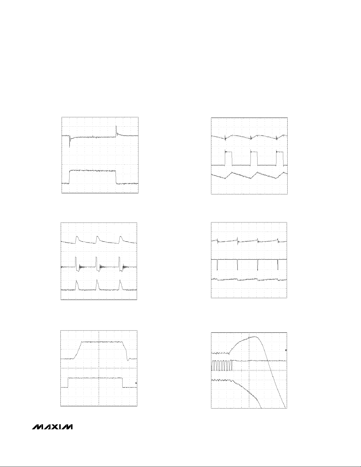
_____________________________Typical Operating Characteristics (continued)
(Circuit of Figure 1, VIN= 7V, TA = +25°C, unless otherwise noted.)
V
OUT
50mV/div
5A LOAD CURRENT
0A
10A
LOAD-TRANSIENT RESPONSE
(1.8V, PWM MODE)
MAX1636 TOC13
100µs/div
V
OUT
20mV/div
V
LX
INDUCTOR
CURRENT
1A
0V
5V
0A
SWITCHING WAVEFORMS
(PWM MODE)
MAX1636 TOC14
1µs/div
V
OUT
50mV/div
V
LX
INDUCTOR
CURRENT
1A
0V
5V
0A
SWITCHING WAVEFORMS
(PFM MODE)
MAX1636 TOC15
20µs/div
V
OUT
= 1.8V
V
OUT
1V/div
V
SHDN
5V/div
STANDBY AND STARTUP RESPONSE
(V
OUT
= 1.8V, NO LOAD)
MAX1636 TOC17
1ms/div
V
OUT
20mV/div
V
LX
INDUCTOR
CURRENT
4A
0
5V
2A
0A
SWITCHING WAVEFORMS
(DROPOUT OPERATION)
MAX1636 TOC16
5µs/div
V
OUT
= 5V
V
OUT
100mV/div
V
DL
INDUCTOR
CURRENT
-5A
0
0
5V
-10A
OVERVOLTAGE-PROTECTION WAVEFORMS
(V
IN
SHORTED TO V
OUT
THROUGH a 0.5Ω RESISTOR)
MAX1636 TOC18
10µs/div

MAX1636
Low-Voltage, Precision Step-Down
Controller for Portable CPU Power
8 _______________________________________________________________________________________
______________________________________________________________Pin Description
NAME FUNCTION
1 CSH Current-Sense Input, High Side
2 CSL Current-Sense Input, Low Side. Also serves as a feedback input in fixed output modes.
PIN
3
RESET
Timed Reset Output. Low for at least 100ms after output voltage is valid, then goes high impedance
(open drain).
4
SHDN
Shutdown Control Input. Puts chip in shutdown or standby mode, depending on OVP (Table 5).
8 SYNC
Oscillator Frequency Select and Synchronization Input. Tie to VCCfor 300kHz operation; tie to GND for
200kHz operation.
7 REF
1.100V Reference Output. Capable of sourcing 50µA for external loads; bypass with a 0.22µF
(min) capacitor.
6 CC Compensation pin. Connect a small capacitor to GND to set the integration time constant.
5 OVP Overvoltage Protection Enable/Disable. Tie to GND to disable OVP; tie to VCCto enable OVP.
13 V+
5V VL Linear-Regulator Input. The VL linear regulator automatically shuts off if V+ is left open or shorted to
VL. Bypass V+ to GND with a 0.1µF capacitor close to the IC.
12 V
CC
Main Supply Voltage Input. Powers the PWM controller, logic, and reference. Input range is +3.15V to
+5.5V.
11 FB
Feedback Input. Tie to GND for fixed 3.3V output; tie to VCCfor fixed 2.5V output; tie to resistor divider for
adjustable mode.
9, 10 GND Analog Ground
15 DL Low-Side Gate-Driver Output
14 VL 5V Linear-Regulator Output. Powers the DL low-side gate driver. Bypass with a 2.2µF (min) capacitor.
20
SKIP
Low-Noise Mode Control. Forces fixed-frequency PWM operation when high.
19 LX Inductor Connection
18 DH High-Side Gate-Driver Output
17 BST Boost-Capacitor Connection
16 PGND Power Ground
______Standard Application Circuit
The basic MAX1636 buck converter (Figure 1) is easily
adapted to meet a wide range of applications with
inputs up to 30V by substituting components from
Table 1. These circuits represent a good set of tradeoffs between cost, size, and efficiency, while staying
within the worst-case specification limits for stressrelated parameters, such as capacitor ripple current.
Do not change the circuits’ switching frequency without
first recalculating component values (particularly inductance value at maximum battery voltage). Adding a
Schottky rectifier across the synchronous rectifier
improves circuit efficiency by approximately 1%. This
rectifier is otherwise not needed because the MOSFET
required typically incorporates a high-speed silicon
diode from drain to source. Use a Schottky rectifier
rated at a DC current equal to at least one-third of the
load current.
 Loading...