

Page 1
查询MAX1626供应商
19-1075; Rev 0; 6/96
EVALUATION KIT MANUAL
FOLLOWS DATA SHEET
High-Efficiency, Step-Down DC-DC Controllers
_______________General Description
The MAX1626/MAX1627 step-down DC-DC switching
controllers provide high efficiency over loads ranging
from 1mA to more than 2A. A unique current-limited,
pulse-frequency-modulated (PFM) control scheme
operates with up to a 100% duty cycle, resulting in very
low dropout voltages. This control scheme eliminates
minimum load requirements and reduces the supply
current under light loads to 90µA (versus 2mA to 10mA
for common pulse-width modulation controllers).
These step-down controllers drive an external P-channel MOSFET, allowing design flexibility for applications
to 12W or higher. Soft-start reduces current surges during start-up. A high switching frequency (up to 300kHz)
and operation in continuous-conduction mode allow the
use of tiny surface-mount inductors. Output capacitor
requirements are also reduced, minimizing PC board
area and system costs.
The output voltage is preset at 5V or 3.3V for the
MAX1626 and adjustable for the MAX1627. Input voltages can be up to 16.5V. The MAX1626/MAX1627 are
functional upgrades for the MAX1649/MAX1651.
________________________Applications
PCMCIA Power Supplies
Personal Digital Assistants
Hand-Held Computers
Portable Terminals
Low-Cost Notebook Computer Supplies
5V to 3.3V Green PC Applications
High-Efficiency Step-Down Regulation
Minimum-Component DC-DC Converters
Battery-Powered Applications
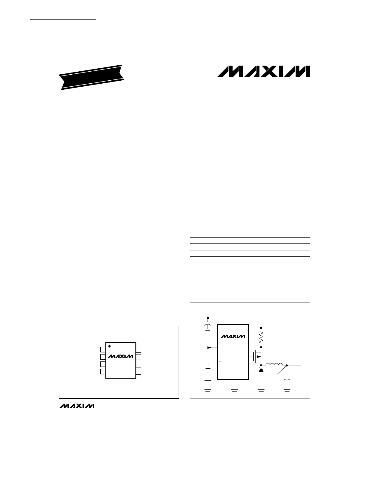
__________________Pin Configuration
TOP VIEW
3/5 (FB)
SHDN
( ) ARE FOR MAX1627
5V/3.3V or Adjustable, 100% Duty-Cycle,
____________________________Features
♦ Low Dropout Voltage
♦ 100% Maximum Duty Cycle
♦ Soft-Start Limits Start-Up Current
♦ Efficiency >90% (3mA to 2A Loads)
♦ Output Power >12.5W
♦ 90µA Max Quiescent Current
♦ 1µA Max Shutdown Current
♦ Up to 300kHz Switching Frequency
♦ 16.5V Max Input Voltage
♦ Output Voltage: 5V/3.3V (MAX1626)
Adjustable (MAX1627)
♦ Current-Limited Control Scheme
______________Ordering Information
TEMP. RANGE PIN-PACKAGE
0°C to +70°C
-40°C to +85°C
0°C to +70°C
V+
MAX1626
CSSHDN
P
3/5
REF
GND
EXT
OUT
Dice*
8 SO
Dice*
OUTPUT
3.3V
OUT
REF
1
2
3
4
MAX1626
MAX1627
SO
PART
MAX1626C/D
MAX1626ESA
MAX1627C/D
MAX1627ESA -40°C to +85°C 8 SO
* Dice are tested at TA= +25°C.
__________Typical Operating Circuit
INPUT
3.3V to 16.5V
8
GND
EXT
7
CS
6
5
V+
ON/OFF
MAX1626/MAX1627
________________________________________________________________
Maxim Integrated Products
1
For free samples & the latest literature: http://www.maxim-ic.com, or phone 1-800-998-8800
Page 2
5V/3.3V or Adjustable, 100% Duty-Cycle,
High-Efficiency, Step-Down DC-DC Controllers
ABSOLUTE MAXIMUM RATINGS
Supply Voltage, V+ to GND.......................................-0.3V, +17V
OUT, FB, 3/5, SHDN, REF, CS, EXT to GND...-0.3V, (V+ + 0.3V)
Maximum Current at REF (I
Maximum Current at EXT (I
Continuous Power Dissipation (T
SO (derate 5.88mW/°C above +70°C)..........................471mW
Stresses beyond those listed under “Absolute Maximum Ratings” may cause permanent damage to the device. These are stress ratings only, and functional
operation of the device at these or any other conditions beyond those indicated in the operational sections of the specifications is not implied. Exposure to
absolute maximum rating conditions for extended periods may affect device reliability.
)..........................................15mA
REF
) ..........................................50mA
EXT
= +70°C)
A
ELECTRICAL CHARACTERISTICS
(V+ = +3V to +16.5V, SHDN = 3/5 = 0V, TA= 0°C to +85°C, unless otherwise noted.)
Operating, no load
V
I+Supply Current into V+
V+ = SHDN = 16.5V (shutdown)
Circuit of Figure 1, 3/5 = V+ (Note 1)
OUT
Circuit of Figure 1, 3/5 = 0V (Note 1)
MAX1626, 3/5 = V+, output forced to 5V
OUT
MAX1627, includes hysteresis
MAX1627
CS
SHDN = 0V or V+
3/5 = 0V or V+
V+ = 5V
Output forced to 0V
Output in regulation
6.0V < V+ < 12.0V, I
30mA < I
LOAD
I
= 0µA
LOAD
REF
REF
≤ 100µA
0µA ≤ I
V+ = 3V to 16.5V, I
MAX1626/MAX1627
Output Voltage
OUT Input Current
CS Threshold Voltage
3/5 Input Voltage High
3/5 Input Voltage Low
3/5 Leakage Current
Minimum EXT Off Time
Reference Voltage
Operating Temperature Range
MAX1626ESA/MAX1627ESA............................-40°C to +85°C
Storage Temperature Range.............................-65°C to +160°C
Lead Temperature (soldering, 10sec).............................+300°C
CONDITIONS
70 90
4.85 5.00 5.15
3.20 3.30 3.40
81012
1.5 2.0 2.5
= 1A
LOAD
< 2.0A, V+ = 8V
= 0µA µV/V10 100REF Line Regulation
LOAD
UNITSMIN TYP MAXSYMBOLPARAMETER
1
V3.0 16.5V+Input Voltage Range
µA
V2.7 2.8Undervoltage Lockout
V
µA24 37 50I
V1.27 1.30 1.33FB Threshold Voltage
nA035FB Leakage Current
µA010CS Input Current
mV85 100 115V
V1.6SHDN Input Voltage High
V0.4SHDN Input Voltage Low
µA±1SHDN Input Current
VV+ - 0.5
V0.5
µA±1
Ω10EXT Resistance
µs
%100EXT Duty-Cycle Limit
mV/V5Line Regulation
mV/A15Load Regulation
V1.27 1.30 1.33V
mV410REF Load Regulation
2 _______________________________________________________________________________________
Page 3
5V/3.3V or Adjustable, 100% Duty-Cycle,
High-Efficiency, Step-Down DC-DC Controllers
ELECTRICAL CHARACTERISTICS
(V+ = +3V to +16.5V, SHDN = 3/5 = 0V, TA= -40°C to +85°C, unless otherwise noted.) (Note 2)
CONDITIONS
Operating, no load
Supply Current into V+
Output Voltage
OUT Input Current
I
V
OUT
V+ = SHDN = 16.5V (shutdown)
Circuit of Figure 1, 3/5 = V+
OUT
Circuit of Figure 1, 3/5 = 0V
MAX1626, 3/5 = V+, output forced to 5V
OUT
MAX1627, includes hysteresis
MAX1627
I
= 0µA
LOAD
Note 1: V+ must exceed V
Note 2: Specifications from 0°C to -40°C are guaranteed by design, not production tested.
to maintain regulation.
OUT
4.80 5.20
3.16 3.44
100
2
MAX1626/MAX1627
UNITSMIN TYP MAXSYMBOLPARAMETER
V3.0 16.5V+Input Voltage
µA
V2.9Undervoltage Lockout
V
µA24 50I
V1.25 1.35FB Threshold Voltage
nA050FB Leakage Current
mV80 120CS Threshold Voltage
V1.25 1.35Reference
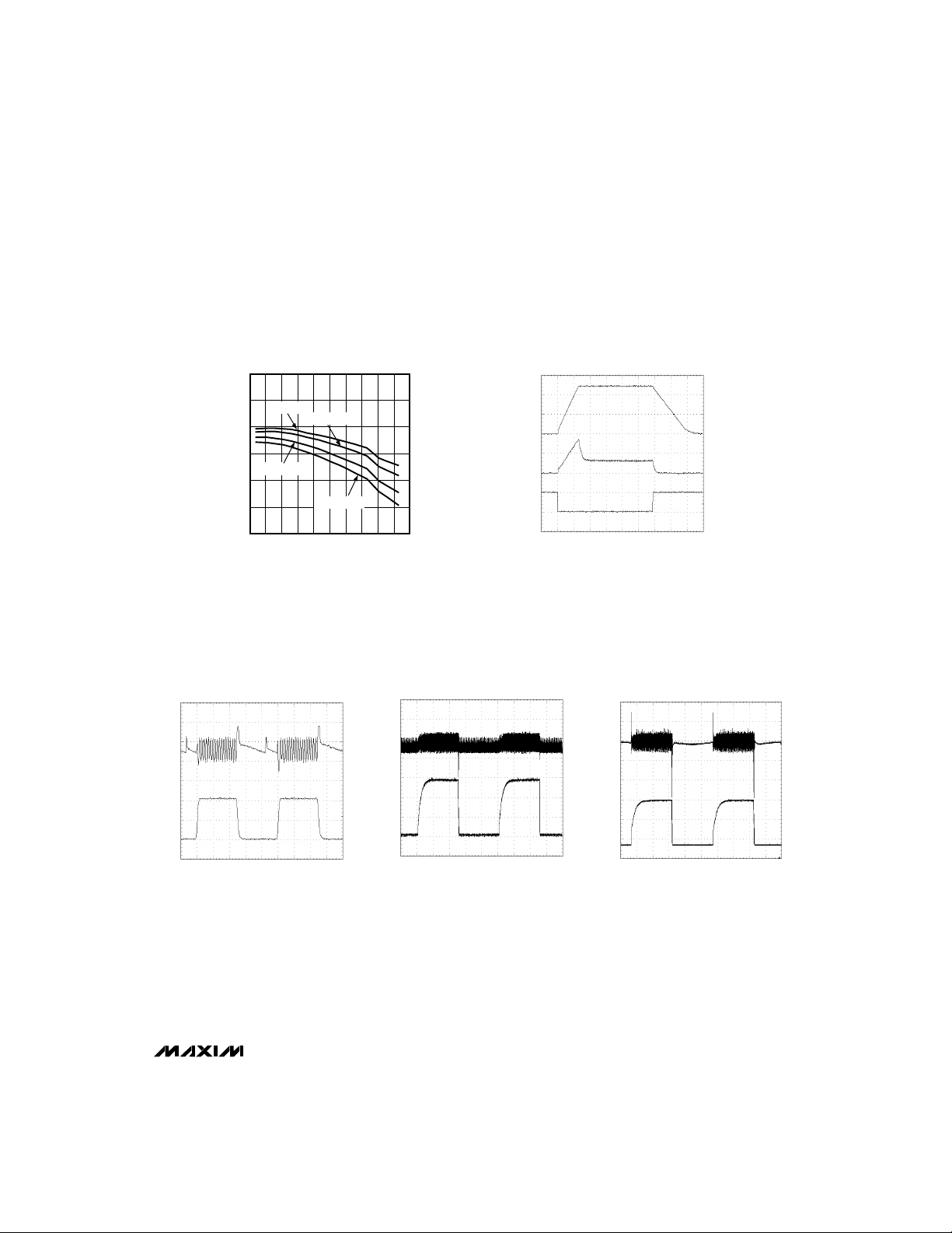
__________________________________________Typical Operating Characteristics
(Circuit of Figure 1, TA= +25°C, unless otherwise noted.)
DROPOUT VOLTAGE
0.45
0.40
0.35
0.30
0.25
0.20
0.15
DROPOUT VOLTAGE (V)
0.10
0.05
0
vs. LOAD CURRENT
3.3V SETTING
= +3.17V
V
OUT
0 0.5 1.0 1.5 2.0 2.5
LOAD (A)
_______________________________________________________________________________________ 3
5V SETTING
= +4.8V
V
OUT
MAX1626-11
EFFICIENCY vs. LOAD CURRENT
(V
= +3.3V)
100
90
A
80
70
60
50
40
EFFICIENCY (%)
30
20
10
CIRCUIT OF FIGURE 1
0
0.1m 100m 11m 10m 10
C
B
LOAD CURRENT (A)
OUT
D E F
A: V+ = +4.3V
B: V+ = +5V
C: V+ = +8V
D: V+ = +10V
E: V+ = +12V
F: V+ = +15V
MAX1626-05
EFFICIENCY (%)
EFFICIENCY vs. LOAD CURRENT
(V
= +5V)
100
90
A
80
70
60
50
40
30
20
10
CIRCUIT OF FIGURE 1
0
0.1m 100m 11m 10m 10
OUT
C
B
LOAD CURRENT (A)
D
E
A: V+ = +6V
B: V+ = +8V
C: V+ = +10V
D: V+ = +12V
E: V+ = +15V
MAX1626-03
Page 4
5V/3.3V or Adjustable, 100% Duty-Cycle,
High-Efficiency, Step-Down DC-DC Controllers
____________________________Typical Operating Characteristics (continued)
(Circuit of Figure 1, TA= +25°C, unless otherwise noted.)
MAX1626 SHUTDOWN CURRENT
0.8
0.7
0.6
0.5
0.4
0.3
0.2
SHUTDOWN CURRENT (µA)
0.1
0
-60
MAX1626/MAX1627
vs. TEMPERATURE
APPLICATION CIRCUIT
SHUTDOWN CURRENT:
A: V+ = +15V
B: V+ = +10V
C: V+ = +4V
MAX1626 SHUTDOWN
CURRENT:
D: V+ = +16V
E: V+ = +4V
-20 0 204060 80 100120
-40
TEMPERATURE (°C)
A
MAX1626-04
B
C
D
EXT OFF TIME (µs)
E
140
MAX1626 EXT OFF TIME
vs. OUTPUT VOLTAGE
12
10
8
6
4
2
0
012345
3/5 = V+
3/5 = GND
OUTPUT VOLTAGE (V)
V+ = +5V
MAX1626-02
12
10
8
6
4
EXT OFF TIME (µs)
2
MAX1627 EXT OFF TIME
vs. FB PIN VOLTAGE
0
0 0.2 0.4 0.6 0.8 1.0 1.2 1.4
FB PIN VOLTAGE (V)
V+ = +5V
MAX1626-03
EXT RISE AND FALL TIMES
50
45
40
35
(ns)
30
FALL
25
AND t
20
RISE
t
15
10
5
0
-60 -40 -20 40 60 140
vs. TEMPERATURE
t
, V+ = +5V
FALL
t
RISE
C
= 1nF
EXT
3/5 = 0V
OUT = 50kHz, 0.3Vp-p
0
20 80
TEMPERATURE (°C)
t
RISE
, t
FALL
3.3V
,
, V+ = +5V
, V+ = +15V
DC
100 120
MAX1626-09
400
350
300
(ns)
250
FALL
200
AND t
150
RISE
t
100
50
EXT RISE AND FALL TIMES
vs. CAPACITANCE
t
, V+ = +15V
RISE
, V+ = +5V
t
FALL
t
, V+ = +5V
RISE
, V+ = +15V
t
0
0 2000 4000
CAPACITANCE (pF)
FALL
MAX1626
V+ QUIESCENT CURRENT
72
70
68
66
(µA)
Q
I
64
62
60
-60
vs. TEMPERATURE
V+ = +16V
V+ = +10V
V+ = +4V
3/5 = 0V
OUT FORCED TO 3.4V
-20 0 204060 80 100120
-40
TEMPERATURE (°C)
MAX1626-01
140
CS TRIP LEVEL vs. TEMPERATURE
115
OUT = 0V
110
105
100
95
CS TRIP LEVEL (mV)
90
85
-60 -40 -20 0 20 40 60 80 100 120 140
TEMPERATURE (°C)
4 _______________________________________________________________________________________
MAX1626-10
MAX1626-12
Page 5
5V/3.3V or Adjustable, 100% Duty-Cycle,
High-Efficiency, Step-Down DC-DC Controllers
____________________________Typical Operating Characteristics (continued)
(Circuit of Figure 1, TA= +25°C, unless otherwise noted.)
MAX1626/MAX1627
REFERENCE OUTPUT VOLTAGE
vs. TEMPERATURE
1.310
1.305
1.300
1.295
1.290
1.285
REFERENCE OUTPUT VOLTAGE (V)
1.280
I
= 0µA
REF
= 50µA
I
REF
-60 -40 -20 0 20 40 60 80 100 120 140
TEMPERATURE (°C)
MAX1626 LOAD-TRANSIENT RESPONSE
A
I
REF
= 10µA
I
REF
= 100µA
MAX1626-15
MAX1626-13
MAX1626 LINE-TRANSIENT RESPONSE
A
MAX1626 SHUTDOWN RESPONSE TIME
AND SUPPLY CURRENT
A
B
C
V+ = 8V, V
A: OUT, 2V/div
B: SUPPLY CURRENT, 1A/div
C: SHDN, 5V/div
500µs/div
= 5V, LOAD = 1A
OUT
LINE-TRANSIENT RESPONSE
FROM 100% DUTY CYCLE
MAX1626-16
A
MAX1626-14
MAX1626-17
B
V+ = 8V, V
A: OUT, 50mV/div, 3.3V DC OFFSET
B: LOAD CURRENT, 1A/div
100µs/div
= 3.3V, LOAD = 30mA to 2A
OUT
_______________________________________________________________________________________
B
V
= 5V, LOAD = 1A, CIN = 33µF
OUT
A: OUT, 100mV/div, 5V DC OFFSET
B: V+ 6V to 12V, 2V/div
5ms/div
B
V
= 3.3V, LOAD = 1A, CIN = 47µF
OUT
A: OUT, 100mV/div, 3.3V DC OFFSET
B: V+ 3.3V to 15V, 5V/div
5ms/div
5
Page 6
5V/3.3V or Adjustable, 100% Duty-Cycle,
High-Efficiency, Step-Down DC-DC Controllers
______________________________________________________________Pin Description
MAX1626
PIN
MAX1627
NAME
Sense input for fixed 5V or 3.3V output operation. OUT is internally connected to an
11
OUT
on-chip voltage divider (MAX1626). It does not supply current. Leave OUT unconnected during adjustable-output operation (MAX1627).
2—
—2
FB
3/5
Feedback Input for adjustable-output operation. Connect to an external voltage
divider between the output and GND (see the
3.3V or 5V Selection. Output voltage is set to 3.3V when this pin is low or 5V when it
is high.
Active-High Shutdown Input. Device is placed in shutdown when SHDN is driven
33
SHDN
high. In shutdown mode, the reference, output, and external MOSFET are turned off.
Connect to GND for normal operation.
MAX1626/MAX1627
V+
REF
1.3V Reference Output. Can source 100µA. Bypass with 0.1µF.44
Positive Supply Input. Bypass with 0.47µF.55
Current-Sense Input. Connect current-sense resistor between V+ and CS. External
66
CS
MOSFET is turned off when the voltage across the resistor equals the current-limit
trip level (around 100mV).
Gate Drive for External P-Channel MOSFET. EXT swings between V+ and GND.77
Ground88
C5
0.47µF
R
SENSE
0.04Ω
U1
LOGIC-LEVEL MOSFET
L1
22µH, 3A
L1: SUMIDA CDRH125-220
D1: NIHON NSQ03A03
U1: MORTOLA MMSF3PO2HD
INPUT
68µF LOW-ESR
TANTALUM
C4
0.1µF
C2
3/5
SHDN
REF
MAX1626
GND
C3
68µF LOW-ESR
TANTALUM
V+
CS
EXT
OUT
D1
EXT
GND
P
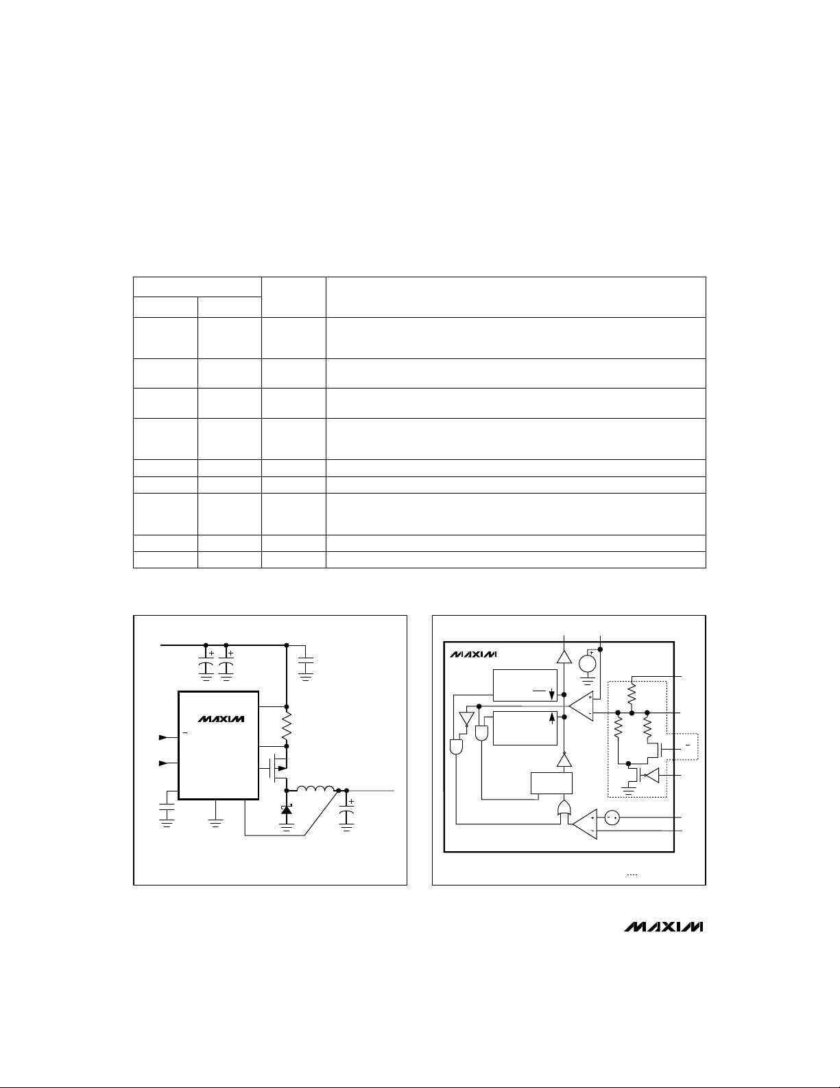
Figure 1. MAX1626 Typical Operating Circuit
OUTPUT
C1
220µF
LOW-ESR
TANTALUM
FUNCTION
Setting the Output Voltage
EXT REF
1.5V
MAX1626
MAX1627
MINIMUM ON-TIME
ONE-SHOT
TRIG
Q
Q
TRIG
MINIMUM OFF-TIME
ONE-SHOT
S
CURRENT-SENSE
COMPARATOR
REF
Q
R
Figure 2. Simplified Functional Diagram
ERROR
COMPARATOR
R2
R1
( ) MAX1627 ONLY
MAX1626 ONLY
section).
OUT
(FB)
R3
3/5
SHDN
V+
CS
6 _______________________________________________________________________________________
Page 7

5V/3.3V or Adjustable, 100% Duty-Cycle,
High-Efficiency, Step-Down DC-DC Controllers
_______________Detailed Description
The MAX1626/MAX1627 are step-down DC-DC controllers designed primarily for use in portable computers and battery-powered devices. Using an external
MOSFET and current-sense resistor allows design flexibility and the improved efficiencies associated with
high-performance P-channel MOSFETs. A unique, current-limited, pulse-frequency-modulated (PFM) control
scheme gives these devices excellent efficiency over
load ranges up to three decades, while drawing around
90µA under no load. This wide dynamic range optimizes the MAX1626/MAX1627 for battery-powered
applications, where load currents can vary considerably as individual circuit blocks are turned on and off to
conserve energy. Operation to a 100% duty cycle
allows the lowest possible dropout voltage, extending
battery life. High switching frequencies and a simple
circuit topology minimize PC board area and component costs. Figure 1 shows a typical operating circuit
for the MAX1626.
PFM Control Scheme
The MAX1626/MAX1627 use a proprietary, third-generation, current-limited PFM control scheme. Improvements
include a reduced current-sense threshold and operation
to a 100% duty cycle. These devices pulse only as needed to maintain regulation, resulting in a variable switching
frequency that increases with the load. This eliminates the
current drain associated with constant-frequency pulsewidth-modulation (PWM) controllers, caused by switching
the MOSFET unnecessarily.
When the output voltage is too low, the error comparator sets a flip-flop, which turns on the external P-channel MOSFET and begins a switching cycle (Figures 1
and 2). As shown in Figure 3, current through the
inductor ramps up linearly, storing energy in a magnetic field while dumping charge into an output capacitor
and servicing the load. When the MOSFET is turned off,
the magnetic field collapses, diode D1 turns on, and
the current through the inductor ramps back down,
transferring the stored energy to the output capacitor
and load. The output capacitor stores energy when the
inductor current is high and releases it when the inductor current is low.
The MAX1626/MAX1627 use a unique feedback and
control system to govern each pulse. When the output
voltage is too low, the error comparator sets a flip-flop,
which turns on the external P-channel MOSFET. The
MOSFET turns off when the current-sense threshold is
exceeded or when the output voltage is in regulation. A
one-shot enforces a 2µs minimum on-time, except in
current limit. The flip-flop resets when the MOSFET
turns off. Otherwise the MOSFET remains on, allowing a
duty cycle of up to 100%. This feature ensures the lowest possible dropout. Once the MOSFET is turned off,
the minimum off-time comparator keeps it off. The minimum off-time is normally 2µs, except when the output is
significantly out of regulation. If the output is low by
30% or more, the minimum off-time increases, allowing
soft-start. The error comparator has 0.5% hysteresis for
improved noise immunity.
In the MAX1626, the 3/5 pin selects the output voltage
(Figure 2). In the MAX1627, external feedback resistors
at FB adjust the output.
Operating Modes
When delivering low and medium output currents, the
MAX1626/MAX1627 operate in discontinuous-conduction mode. Current through the inductor starts at zero,
rises as high as the peak current limit set by the current- sense resistor, then ramps down to zero during
each cycle (Figure 3). Although efficiency is still excellent, output ripple increases and the switch waveform
exhibits ringing. This ringing occurs at the resonant frequency of the inductor and stray capacitance, due to
residual energy trapped in the core when the commutation diode (D1 in Figure 1) turns off. It is normal and
poses no operational problems.
When delivering high output currents, the MAX1626/
MAX1627 operate in continuous-conduction mode
(Figure 4). In this mode, current always flows through
the inductor and never ramps to zero. The control circuit adjusts the switch duty cycle to maintain regulation
without exceeding the peak switching current set by
the current-sense resistor. This provides reduced output ripple and high efficiency.
100% Duty Cycle and Dropout
The MAX1626/MAX1627 operate with a duty cycle up
to 100%. This feature extends usable battery life by
turning the MOSFET on continuously when the supply
voltage approaches the output voltage. This services
the load when conventional switching regulators with
less than 100% duty cycle would fail. Dropout voltage
is defined as the difference between the input and output voltages when the input is low enough for the output to drop out of regulation. Dropout depends on the
MOSFET drain-to-source on-resistance, current-sense
resistor, and inductor series resistance, and is proportional to the load current:
Dropout Voltage=
I x R + R + R
OUT DS(ON) SENSE INDUCTOR
[]
MAX1626/MAX1627
_______________________________________________________________________________________ 7
Page 8

5V/3.3V or Adjustable, 100% Duty-Cycle,
High-Efficiency, Step-Down DC-DC Controllers
A
B
C
0A
CIRCUIT OF FIGURE 1, V+ = 8V, V
A: MOSFET DRAIN, 5V/div
B: OUT, 50mV/div, 5V DC OFFSET
MAX1626/MAX1627
Figure 3. Discontinuous-Conduction Mode, Light-Load-Current
Waveform
C: INDUCTOR CURRENT, 1A/div
10µs/div
= 5V, LOAD = 100mA
OUT
EXT Drive Voltage Range
EXT swings from V+ to GND and provides the gate
drive for an external P-channel power MOSFET. A higher supply voltage increases the gate drive to the
MOSFET and reduces on-resistance (R
External Switching Transistor
section.
DS(ON)
Quiescent Current
The device’s typical quiescent current is 70µA.
However, actual applications draw additional current to
supply MOSFET switching currents, OUT pin current, or
external feedback resistors (if used), and both the diode
and capacitor leakage currents. For example, in the circuit of Figure 1, with V+ at 7V and V
at 5V, typical
OUT
no-load supply current for the entire circuit is 84µA.
When designing a circuit for high-temperature operation, select a Schottky diode with low reverse leakage.
Shutdown Mode
When SHDN is high, the device enters shutdown mode.
In this mode, the feedback and control circuit, reference,
and internal biasing circuitry are turned off. EXT goes
high, turning off the external MOSFET. The shutdown
supply current drops to less than 1µA. SHDN is a logiclevel input. Connect SHDN to GND for normal operation.
Reference
The 1.3V reference is suitable for driving external loads,
such as an analog-to-digital converter. It has a guaranteed 10mV maximum load regulation while sourcing load
currents up to 100µA. The reference is turned off during
). See
A
B
C
0A
CIRCUIT OF FIGURE 1, V+ = 8V, V
A: MOSFET DRAIN, 5V/div
B: OUT, 50mV/div, 5V DC OFFSET
C: INDUCTOR CURRENT, 1A/div
Figure 4. Continuous-Conduction Mode, Heavy-Load-Current
Waveform
10µs/div
= 5V, LOAD = 1.5A
OUT
shutdown. Bypass the reference with 0.1µF for normal
operation. Place the bypass capacitor within 0.2 inches
(5mm) of REF, with a direct trace to GND (Figure 7).
Soft-Start
Soft-start reduces stress and transient voltage slumps
on the power source. When the output voltage is near
ground, the minimum off-time is lengthened to limit peak
switching current. This compensates for reduced negative inductor current slope due to low output voltages.
________________Design Information
The MAX1626’s output voltage can be selected to 3.3V
or 5V under logic control by using the 3/5 pin. The 3/5
pin requires less than 0.5V to ensure a 3.3V output, or
more than (V+ - 0.5)V to guarantee a 5V output. The
voltage sense pin (OUT) must be connected to the output for the MAX1626.
The MAX1627’s output voltage is set using two resistors, R2 and R3 (Figure 5), which form a voltage divider
between the output and GND. R2 is given by:
where V
REF
has a maximum value of 50nA, large values (10kΩ to
200kΩ) can be used for R3 with no significant accuracy
loss. For 1% error, the current through R2 should be at
Setting the Output Voltage
R2= R3 x
V
V
OUT
REF
−
1
= 1.3V. Since the input bias current at FB
8 _______________________________________________________________________________________
Page 9

5V/3.3V or Adjustable, 100% Duty-Cycle,
High-Efficiency, Step-Down DC-DC Controllers
least 100 times FB’s input bias current. Capacitor C
is used to compensate the MAX1627 for even switching. Values between 0pF and 330pF work for many
applications. See the
Compensation
Stability and MAX1627 Feedback
section for details.
Current-Sense-Resistor Selection
The current-sense comparator limits the peak switching
current to VCS/R
SENSE
, where R
SENSE
is the value of
the current-sense resistor and VCSis the current-sense
threshold. VCSis typically 100mV, but can range from
85mV to 115mV. Minimizing the peak switching current
will increase efficiency and reduce the size and cost of
external components. However, since available output
current is a function of the peak switching current, the
peak current limit must not be set too low.
Set the peak current limit above 1.3 times the maximum
load current by setting the current-sense resistor to:
V
R =
CS
1.3 x I
CS(MIN)
OUT(MAX)
Alternatively, select the current-sense resistor for 5V
and 3.3V output applications using the current-sense
resistor graphs in Figures 6a and 6b. The current-sense
resistor’s power rating should be 20% higher than:
2
V
R =
POWER RATING (W)
CS MAX()
R
CS
Standard wire-wound resistors have an inductance
high enough to degrade performance, and are not recommended. Surface-mount (chip) resistors have very
little inductance and are well suited for use as current-
3.5
V
= 5V
OUT
3.0
2.5
2.0
1.5
1.0
MAXIMUM OUTPUT CURRENT (A)
0.5
0
4.5 5.55.0 6.0 1210 14 16
R
SENSE
R
SENSE
R
SENSE
R
SENSE
INPUT VOLTAGE (V)
= 0.03Ω
= 0.04Ω
= 0.05Ω
= 0.1Ω
R2
C
R2
FROM
OUTPUT
R2
TO FB
R3
Figure 5. Adjustable-Output Operation Using the MAX1627
sense resistors. Power metal-strip resistors feature
1/2W and 1W power dissipation, 1% tolerance, and
inductance below 5nH. Resistance values between
10mΩ and 500mΩ are available.
Inductor Selection
The essential parameters for inductor selection are
inductance and current rating. The MAX1626/MAX1627
operate with a wide range of inductance values. In many
applications, values between 10µH and 68µH take best
advantage of the controller’s high switching frequency.
Calculate the minimum inductance value as follows:
V+ - V
()
L =
(MIN)
(MAX) OUT
V
()
CS MIN
R
CS
where 2µs is the minimum on-time. Inductor values
between two and six times L
3.5
V
= 3.3V
OUT
3.0
2.5
2.0
1.5
1.0
MAXIMUM OUTPUT CURRENT (A)
0.5
0
3.0 4.03.5 4.5 1210 14 16
INPUT VOLTAGE (V)
are recommended.
(MIN)
R
= 0.03Ω
SENSE
R
= 0.04Ω
SENSE
R
= 0.05Ω
SENSE
R
= 0.1Ω
SENSE
xs
2µ
MAX1626/MAX1627
Figure 6a. MAX1626 5V-Operation Current-Sense Resistor
Graph
_______________________________________________________________________________________ 9
Figure 6b. MAX1626 3.3V-Operation Current-Sense Resistor
Graph
Page 10

5V/3.3V or Adjustable, 100% Duty-Cycle,
High-Efficiency, Step-Down DC-DC Controllers
With high inductor values, the MAX1626/MAX1627 will
begin continuous-conduction operation at a lower fraction of the full load (see
Detailed Description
). Low-value
inductors may be smaller and less expensive, but they
result in greater peak current overshoot due to currentsense comparator propagation delay. Peak-current
overshoot reduces efficiency and could cause the external components’ current ratings to be exceeded.
The inductor’s saturation and heating current ratings
must be greater than the peak switching current to prevent overheating and core saturation. Saturation occurs
when the inductor’s magnetic flux density reaches the
maximum level the core can support, and inductance
starts to fall. The heating current rating is the maximum
DC current the inductor can sustain without overheating.
The peak switching current is the sum of the current limit
set by the current-sense resistor and overshoot during
current-sense comparator propagation delay.
MAX1626/MAX1627
I =
PEAK
V
CS
R
CS
+−
VV 1s
()
+
OUT
L
×µ
1µs is the worst-case current-sense comparator propagation delay.
Inductors with a core of ferrite, Kool Mu™, METGLAS™,
or equivalent, are recommended. Powder iron cores
are not recommended for use with high switching
frequencies. For optimum efficiency, the inductor windings’ resistance should be on the order of the currentsense resistance. If necessary, use a toroid, pot-core,
KOOL Mu is a trademark of Magnetics.
METGLAS is a trademark of Allied Signal.
or shielded-core inductor to minimize radiated noise.
Table 1 lists inductor types and suppliers for various
applications.
External Switching Transistor
The MAX1626/MAX1627 drive P-channel enhancementmode MOSFETs. The EXT output swings from GND to
the voltage at V+. To ensure the MOSFET is fully on,
use logic-level or low-threshold MOSFETs when the
input voltage is less than 8V. Tables 1 and 2 list recommended suppliers of switching transistors.
Four important parameters for selecting a P-channel
MOSFET are drain-to-source breakdown voltage, current rating, total gate charge (Qg), and R
drain-to-source breakdown voltage rating should be at
least a few volts higher than V+. Choose a MOSFET
with a maximum continuous drain current rating higher
than the peak current limit:
V
CS MAX
I
D(MAX LIM MAX
I
≥=
)()
()
R
SENSE
The Qg specification should be less than 100nC to
ensure fast drain voltage rise and fall times, and reduce
power losses during transition through the linear region.
Qgspecifies all of the capacitances associated with
charging the MOSFET gate. EXT pin rise and fall times
vary with different capacitive loads, as shown in the
Typical Operating Characteristics
. R
DS(ON)
as low as practical to reduce power losses while the
MOSFET is on. It should be equal to or less than the
current-sense resistor.
DS(ON)
should be
. The
Table 1. Component Selection Guide
PRODUCTION
METHOD
Surface Mount
Miniature
Through-Hole
Low-Cost
Through-Hole
10 ______________________________________________________________________________________
INDUCTORS CAPACITORS DIODES
Sumida
CDRH125-470 (1.8A)
CDRH125-220 (2.2A)
CoilCraft
DO3316-473 (1.6A)
DO3340-473 (3.8A)
Sumida
RCH875-470M (1.3A)
CoilCraft
PCH-45-473 (3.4A)
AVX
TPS series
Sprague
595D series
Sanyo
OS-CON series
low-ESR organic
semiconductor
Nichicon
PL series
low-ESR electrolytics
United Chemi-Con
LXF series
Motorola
MBRS340T3
Nihon
NSQ series
Motorola
1N5817 to
1N5823
CURRENT-SENSE
RESISTORS
Dale
WSL series
IRC
LRC series
IRC
OAR series
Siliconix
Little Foot series
Motorola
medium-power
surface-mount products
Motorola
Motorola
TMOS power MOSFETs
MOSFETS
Page 11

5V/3.3V or Adjustable, 100% Duty-Cycle,
High-Efficiency, Step-Down DC-DC Controllers
Table 2. Component Suppliers
COMPANY PHONE FAX
AVX USA or (803) 626-3123
Coilcraft USA (847) 639-6400 (847) 639-1469
Coiltronics USA (516) 241-7876 (516) 241-9339
Dale USA (605) 668-4131 (605) 665-1627
International
Rectifier
IRC USA (512) 992-7900 (512) 992-3377
Motorola USA (602) 303-5454 (602) 994-6430
Nichicon USA (847) 843-7500 (847) 843-2798
Nihon USA (805) 867-2555 (805) 867-2698
Sanyo USA (619) 661-6835 (619) 661-1055
Siliconix USA or (408) 970-3950
Sprague USA (603) 224-1961 (603) 224-1430
Sumida USA (847) 956-0666 (847) 956-0702
United
Chemi-Con
USA (310) 322-3331 (310) 322-3332
Japan 81-7-5231-8461 81-7-5256-4158
Japan 81-3-3494-7411 81-3-3494-7414
Japan 81-7-2070-6306 81-7-2070-1174
Japan 81-3-3607-5111 81-3-3607-5144
USA (714) 255-9500 (714) 255-9400
The MAX1626/MAX1627’s high switching frequency
demands a high-speed rectifier. Schottky diodes, such
as the 1N5817–1N5822 family or surface-mount equivalents, are recommended. Ultra-high-speed rectifiers
with reverse recovery times around 50ns or faster, such
as the MUR series, are acceptable. Make sure that the
diode’s peak current rating exceeds the peak current
limit set by R
SENSE
exceeds V+. Schottky diodes are preferred for heavy
loads due to their low forward voltage, especially in
low-voltage applications. For high-temperature applications, some Schottky diodes may be inadequate due to
their high leakage currents. In such cases, ultra-highspeed rectifiers are recommended, although a Schottky
diode with a higher reverse voltage rating can often
provide acceptable performance.
Choose filter capacitors to service input and output
peak currents with acceptable voltage ripple.
Equivalent series resistance (ESR) in the capacitor is a
major contributor to output ripple, so low-ESR capacitors are recommended. Sanyo OS-CON capacitors are
(803) 946-0690
(800) 282-4975
(408) 988-8000
(800) 554-5565
Diode Selection
, and that its breakdown voltage
Capacitor Selection
best, and low-ESR tantalum capacitors are second
best. Low-ESR aluminum electrolytic capacitors are tolerable, but do not use standard aluminum electrolytic
capacitors.
Voltage ripple is the sum of contributions from ESR and
the capacitor value:
V
≈+
RIPPLE
VV
,,
RIPPLE ESR RIPPLE C
To simplify selection, assume initially that two-thirds of
the ripple results from ESR and one-third results from
capacitor value. Voltage ripple as a consequence of
ESR is approximated by:
V
RIPPLE,ESR
≈ ()()R
ESRIPEAK
Estimate input and output capacitor values for given
voltage ripple as follows:
2
1
LI
∆
L
2
=
VV
,
RIPPLE CIN IN
=
VV
RIPPLE COUT OUTININ OUT
2
1
LI
∆
L
2
,
V
−
VV
is the change in inductor current (around
under moderate loads).
where I
0.5I
PEAK
C
IN
C
OUT
∆L
These equations are suitable for initial capacitor selection; final values should be set by testing a prototype or
evaluation kit. When using tantalum capacitors, use
good soldering practices to prevent excessive heat
from damaging the devices and increasing their ESR.
Also, ensure that the tantalum capacitors’ surge-current
ratings exceed the start-up inrush and peak switching
currents.
Pursuing output ripple lower than the error comparator’s hysteresis (0.5% of the output voltage) is not practical, since the MAX1626/MAX1627 will switch as
needed, until the output voltage crosses the hysteresis
threshold. Choose an output capacitor with a working
voltage rating higher than the output voltage.
The input filter capacitor reduces peak currents drawn
from the power source and reduces noise and voltage
ripple on V+ and CS, caused by the circuit’s switching
action. Use a low-ESR capacitor. Two smaller-value
low-ESR capacitors can be connected in parallel for
lower cost. Choose input capacitors with working voltage ratings higher than the maximum input voltage.
Place a surface-mount ceramic capacitor very close to
V+ and GND, as shown in Figure 7. This capacitor
bypasses the MAX1626/MAX1627, and prevents spikes
and ringing on the power source from obscuring the
MAX1626/MAX1627
______________________________________________________________________________________ 11
Page 12

5V/3.3V or Adjustable, 100% Duty-Cycle,
High-Efficiency, Step-Down DC-DC Controllers
current feedback signal and causing jitter. 0.47µF is
recommended. Increase the value as necessary in
high-power applications.
Bypass REF with 0.1µF. This capacitor should be
placed within 0.2 inches (5mm) of the IC, next to REF,
with a direct trace to GND (Figure 7).
Layout Considerations
High-frequency switching regulators are sensitive to PC
board layout. Poor layout introduces switching noise into
the current and voltage feedback signals, resulting in jitter, instability, or degraded performance. The currentsense resistor must be placed within 0.2 inches (5mm)
of the controller IC, directly between V+ and CS. Place
voltage feedback resistors (MAX1627) next to the FB pin
(no more than 0.2") rather than near the output. Place
the 0.47µF input and 0.1µF reference bypass capacitors
within 0.2 inches (5mm) of V+ and REF, and route
directly to GND. Figure 7 shows the recommended lay-
MAX1626/MAX1627
out and routing for these components.
High-power traces, highlighted in the
Circuit
(Figure 1), should be as short and as wide as
possible. The supply-current loop (formed by C2, C3,
R
, U1, L1, and C1) and commutation-current loop
SENSE
(D1, L1, and C1) should be as tight as possible to
reduce radiated noise. Place the anode of the commutation diode (D1) and the ground pins of the input and
output filter capacitors close together, and route them to
a common “star-ground” point. Place components and
route ground paths so as to prevent high currents from
causing large voltage gradients between the ground pin
of the output filter capacitor, the controller IC, and the
reference bypass capacitor. Keep the extra copper on
the component and solder sides of the PC board, rather
than etching it away, and connect it to ground for use as
a pseudo-ground plane. Refer to the MAX1626
Evaluation Kit manual for a two-layer PC board example.
Typical Operating
Stability and MAX1627 Feedback
Compensation
Use proper PC board layout and recommended external components to ensure stable operation. In oneshot, sequenced PFM DC-DC converters, instability is
manifested as “Motorboat Instability.” It is usually
caused by excessive noise on the current or voltage
feedback signals, ground, or reference, due to poor PC
board design or external component selection.
Motorboat instability is characterized by grouped
switching pulses with large gaps and excessive lowfrequency output ripple. It is normal to see some
grouped switching pulses during the transition from
discontinuous to continuous current mode. This effect
is associated with small gaps between pulse groups
MAX1626
4x
SCALE
C
REF
C
V+ BYPASS
Figure 7. Recommended Placement and Routing of the
Current-Sense Resistor, 0.1µF Reference, and 0.47µF Input
Bypass Capacitors
and output ripple similar to or less than that seen during no-load conditions.
Instability can also be caused by excessive stray capacitance on FB when using the MAX1627. Compensate for
this by adding a 0pF to 330pF feed-forward capacitor
across the upper feedback resistor (R2 in Figure 5).
MAX1626/MAX1627 vs.
MAX1649/MAX1651 vs.
MAX649/MAX651
The MAX1626/MAX1627 are specialized, third-generation upgrades to the MAX649/MAX651 step-down controllers. They feature improved efficiency, a reduced
current-sense threshold (100mV), soft-start, and a
100% duty cycle for lowest dropout. The MAX649/
MAX651 have a two-step (210mV/110mV) currentsense threshold. The MAX1649/MAX1651 are secondgeneration upgrades with a 96.5% maximum duty cycle
for improved dropout performance and a reduced current-sense threshold (110mV) for higher efficiency,
especially at low input voltages. The MAX1649/
MAX1651 are preferable for special applications where
a 100% duty cycle is undesirable, such as flyback and
SEPIC circuits.
Since the MAX1626’s pinout is similar to those of the
MAX649 and MAX1649 family parts, the MAX1626 can
be substituted (with minor external component value
changes) into fixed-output mode applications, provided
the PC board layout is adequate. The MAX1627 can
also be substituted when MAX649 or MAX1649 family
parts are used in adjustable mode, but the feedback
resistor values must be changed, since the MAX1627
has a lower reference voltage (1.3V vs. 1.5V). Reduce
the current-sense resistor value by 50% when substituting for the MAX649 or MAX651.
R
SENSE
12 ______________________________________________________________________________________
Page 13

5V/3.3V or Adjustable, 100% Duty-Cycle,
High-Efficiency, Step-Down DC-DC Controllers
INPUT
68µF LOW-ESR
TANTALUM
C2
68µF LOW-ESR
TANTALUM
C3
C5
0.47µF
INPUT
68µF LOW-ESR
TANTALUM
C2
C3
0.47µF
MAX1626/MAX1627
V+
R
SENSE
0.15Ω
U1
LOGIC-LEVEL MOSFET
P
22µH, 3A
D1
L1: SUMIDA CDRH125-220
D1: NIHON NSQ03A03
C
R2
U1: MOTOROLA MMSF3P02HD
L1
ADJUSTABLE
OUTPUT
C1
220µF
LOW-ESR
TANTALUM
0.1µF
C4
N.C.
MAX1627
OUT
SHDN
REF
GND FB
CS
EXT
R3 R2
Figure 8. MAX1627 Typical Operating Circuit
________________________Applications
The MAX1626/MAX1627 typical operating circuits
(Figures 1 and 8) are designed to output 2A at a 5V
output voltage. The following circuits provide examples
and guidance for other applications.
When designing a low-power, battery-based application, choose an external MOSFET with low gate capacitance (to minimize switching losses), and use a low
peak current limit to reduce I2R losses. The circuit in
Figure 9 is optimized for 0.5A.
The circuit in Figure 10 outputs 6A at 2.5V from a 5V or
3.3V input. High-current design is difficult, and board
layout is critical due to radiated noise, switching transients, and voltage gradients on the PC board traces.
Figure 11 is a recommended PC board design. Choose
the external MOSFET to minimize R
gate-charge factor below the MAX1626/MAX1627’s
drive capability (see Ext Rise and Fall Times vs.
Capacitance graph in the
Characteristics
and fall times will contribute to efficiency losses. For
higher efficiencies, especially at low output voltages,
the MAX796 family of step-down controllers with synchronous rectification is recommended.
Micropower Step-Down Converter
High-Current Step-Down Converter
. Keep the
DS(ON)
Typical Operating
). Otherwise, increased MOSFET rise
V+
MAX1626
0.1µF
3/5
SHDN
REF
C4
GND
CS
EXT
OUT
D1
Figure 9. 0.5A Step-Down Converter
3V TO 6V
INPUT
MAX1627
GND
21.5k, 1%
R3
100µF
C5
C6
0.1µF
V+
CS
EXT
FB
Q1
LOGIC-LEVEL MOSFET
P
2.7µH >8A
D1
R2
20k, 1%
C1–C3: SANYO OS-CON 220µF, 6.3V
C
R2
C4, C5: SANYO OS-CON 100
220pF
RCS1, RCS2: 0.025Ω DALE WSL-2512
Q1: MOTOROLA MTB50PO3HDL
D1: NIEC C10T04Q
L1: SUMIDA CDRH127-2R7NC
C10
0.1µF
100µF
N.C.
C4
OUT
SHDN
REF
Figure 10. 6A Step-Down Converter
R
SENSE
0.15Ω
U1
LOGIC-LEVEL MOSFET
P
L1
68µH, 0.7A
L1: SUMIDA CDR1053-680
D1: MOTOROLA MBRS130T3
U1: MOTOROLA MMSF3P02HD
C8
C7
1.0µF
0.1µF
R
, R
CS1
CS2
0.025Ω
L1
C2
C1
220µF
220µF
OUTPUT
C1
100µF
LOW-ESR
TANTALUM
C9
1.0µF
OUTPUT
2.5V, 6A
C3
220µF
µF, 20V
______________________________________________________________________________________ 13
Page 14

5V/3.3V or Adjustable, 100% Duty-Cycle,
High-Efficiency, Step-Down DC-DC Controllers
VIA
VIAS
MAX1626/MAX1627
VIA
COMPONENT PLACEMENT GUIDE—COMPONENT SIDE
COPPER ROUTING—BACK SIDE
COPPER ROUTING—FRONT SIDE
Figure 11. Recommended PC Board Design for 6A Step-Down Converter
14 ______________________________________________________________________________________
Page 15

5V/3.3V or Adjustable, 100% Duty-Cycle,
High-Efficiency, Step-Down DC-DC Controllers
___________________Chip Topography
GNDGNDOUT
EXT
3/5
(FB)
0.105"
(2.63mm)
MAX1626/MAX1627
SHDN
REF
0.081"
(2.06mm)
( ) ARE FOR MAX1627
TRANSISTOR COUNT: 375
SUBSTRATE CONNECTED TO V+
CS
V
CC
______________________________________________________________________________________ 15
Page 16

5V/3.3V or Adjustable, 100% Duty-Cycle,
High-Efficiency, Step-Down DC-DC Controllers
________________________________________________________Package Information
INCHES MILLIMETERS
DIM
D
A
0.101mm
e
A1
B
MAX1626/MAX1627
0.004in.
HE
C
L
Narrow SO
SMALL-OUTLINE
PACKAGE
(0.150 in.)
0°-8°
A1
DIM
D
D
D
A
B
C
E
e
H
L
PINS
MAX
MIN
0.069
0.053
0.010
0.004
0.019
0.014
0.010
0.007
0.157
0.150
0.228
0.016
8
14
16
0.244
0.050
INCHES MILLIMETERS
MIN
MAX
0.189
0.197
0.337
0.344
0.386
0.394
MIN
1.35
0.10
0.35
0.19
3.80
5.80
0.40
MIN
4.80
8.55
9.80
1.270.050
MAX
1.75
0.25
0.49
0.25
4.00
6.20
1.27
MAX
5.00
8.75
10.00
21-0041A
16 ______________________________________________________________________________________
Page 17

Copyright © Each Manufacturing Company.
All Datasheets cannot be modified without permission.
This datasheet has been download from :
www.AllDataSheet.com
100% Free DataSheet Search Site.
Free Download.
No Register.
Fast Search System.
www.AllDataSheet.com
 Loading...