MAX1623
3A, Low-Voltage, Step-Down Regulator with
Synchronous Rectification and Internal Switches
________________________________________________________________
Maxim Integrated Products
1
EVALUATION KIT MANUAL
FOLLOWS DATA SHEET
General Description
The MAX1623 switch-mode buck regulator with synchronous rectification provides local CPU and bus-termination power in notebook and desktop computers.
An internal 55mΩ (typ), 3A PMOS power switch and
60mΩ (typ), 3A NMOS synchronous-rectifier switch
deliver continuous load currents up to 3A from a 5V
supply with 95% typical efficiency. Output accuracy is
±1%, including line and load regulation.
The MAX1623 features constant-off-time, current-mode
pulse-width-modulation (PWM) control with switching
frequencies as high as 350kHz. An external resistor at
the TOFF pin sets the off-time, allowing optimum design
flexibility in terms of switching frequency, output switching noise, and inductor size. This device is available in
a space-saving 20-pin SSOP package.
________________________Applications
5V to 3.3V Conversion
Notebook Computer CPU I/O Supply
Desktop Computer Bus-Termination Supply
CPU Daughter Card Supply
DSP Supply
____________________________Features
♦ ±1% Output Accuracy, Including Line and Load
Regulation
♦ 94% Efficiency
♦ Internal Switches
55mΩ PMOS Power Switch
60mΩ NMOS Synchronous-Rectifier Switch
♦ Guaranteed 3A Load Capability
♦ Minimal External Components
♦ Pin-Selectable Fixed 3.3V, 2.5V, or
Adjustable (1.1V to 3.8V) Output Voltage
♦ +4.5V to +5.5V Input Voltage Range
♦ 400µA (typ) Supply Current
♦ <1µA Shutdown Supply Current
♦ Constant-Off-Time PWM Operation
♦ Switching Frequencies Up to 350kHz
♦ Idle Mode™ Operation at Light Loads
♦ Thermal Shutdown Protection
♦ Available in 20-Pin SSOP
20
19
18
17
16
15
14
13
1
2
3
4
5
6
7
8
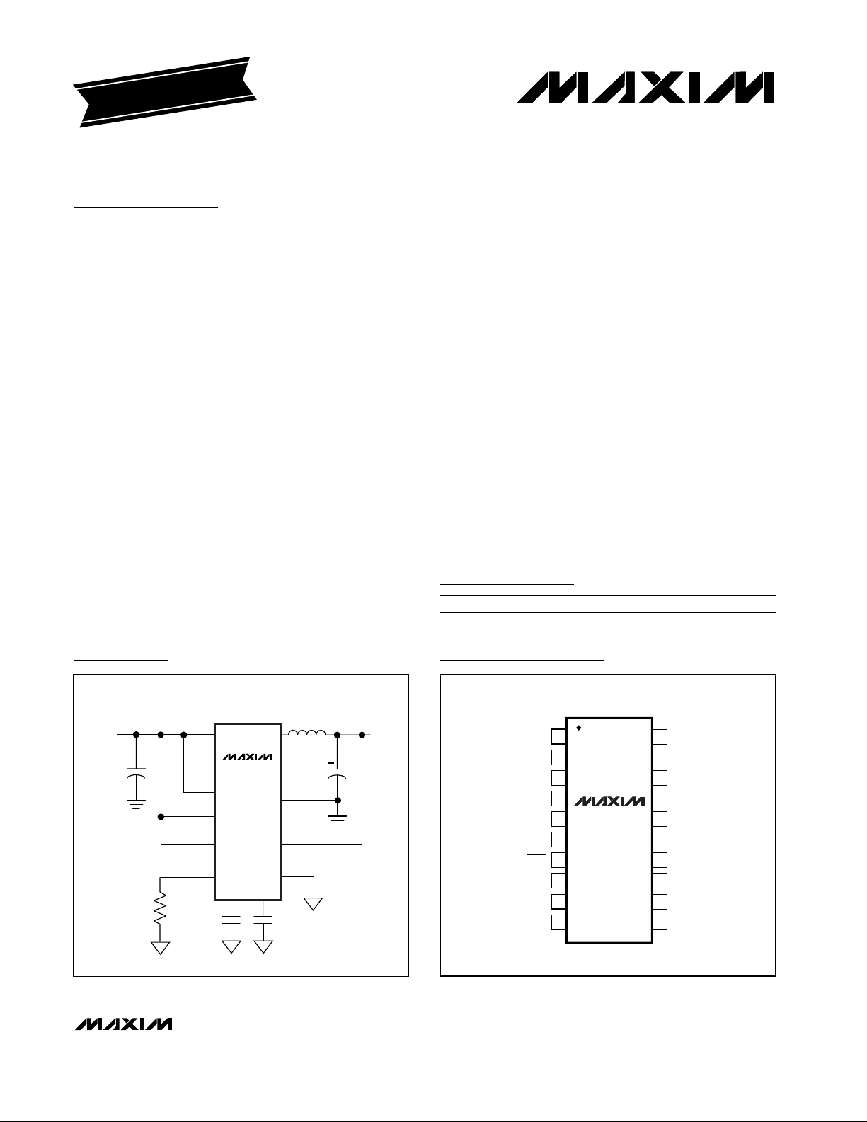
LX
PGND
LX
PGND
IN
LX
IN
LX
TOP VIEW
LX
PGND
V
CC
COMPFBSEL
IN
LX
12
11
9
10
REF
GNDFB
TOFF
MAX1623
SSOP
SHDN
Pin Configuration
+5V
INPUT
MAX1623
+2.5V
OUTPUT
IN LX
PGND
GND
FB
REFCOMP
FBSEL
V
CC
TOFF
SHDN
Typical Operating Circuit
19-1436; Rev 1; 9/99
PART
MAX1623EAP -40°C to +85°C
TEMP. RANGE PIN-PACKAGE
20 SSOP
Ordering Information
Idle Mode is a trademark of Maxim Integrated Products.
For free samples & the latest literature: http://www.maxim-ic.com, or phone 1-800-998-8800.
For small orders, phone 1-800-835-8769.

MAX1623
3A, Low-Voltage, Step-Down Regulator with
Synchronous Rectification and Internal Switches
2 _______________________________________________________________________________________
ABSOLUTE MAXIMUM RATINGS
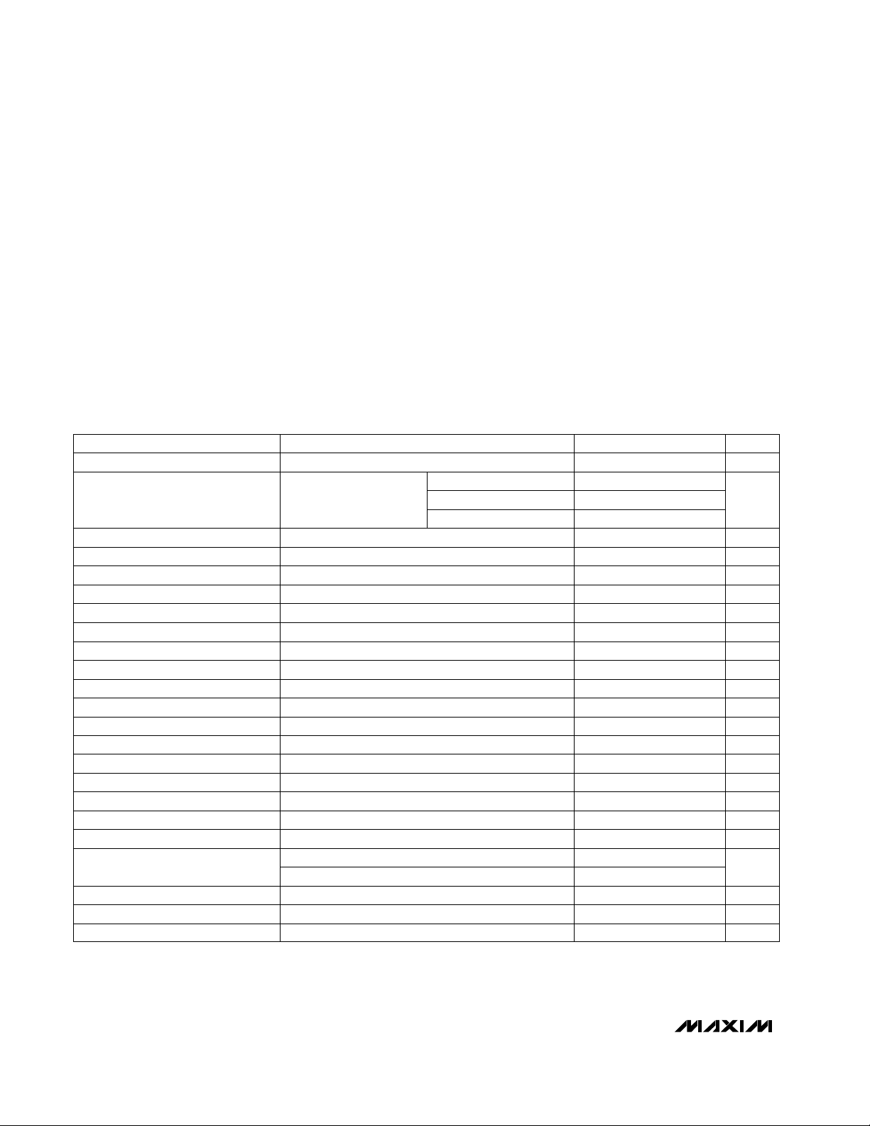
ELECTRICAL CHARACTERISTICS
(VIN= VCC= +5V, FBSEL unconnected, R
TOFF
= 110kΩ, TA= 0°C to +85°C, unless otherwise noted. Typical values are at T
A
=
+25°C.)
Stresses beyond those listed under “Absolute Maximum Ratings” may cause permanent damage to the device. These are stress ratings only, and functional
operation of the device at these or any other conditions beyond those indicated in the operational sections of the specifications is not implied. Exposure to
absolute maximum rating conditions for extended periods may affect device reliability.
IN to PGND .....................................................................0V to 6V
V
CC
to GND ................................................................-0.3V to 6V
PGND to GND.....................................................................±0.5V
IN to V
CC
.............................................................................±0.5V
LX to PGND.................................................................-0.5V to 6V
SHDN to GND .............................................................-0.3V to 6V
REF, FBSEL, COMP, FB, TOFF to GND .....-0.3V to (V
CC
+ 0.3V)
REF Short to GND ......................................................Continuous
Continuous Power Dissipation (T
A
= +70°C) (with part mounted
on 1 sq. inch of one ounce copper)
20-Pin SSOP (derate 22mW/°C above +70°C) ................1.3W
Operating Temperature Range ...........................-40°C to +85°C
Storage Temperature Range .............................-65°C to +150°C
Lead Temperature (soldering, 10sec) .............................+300°C
SHDN = GND or V
CC
FBSEL = REF
FBSEL = GND
VIN= 4.5V to 5.5V,
I
LOAD
= 0 to 3A
(Note 1)
FBSEL = GND, adjustable output mode, VFB= 1.2V
VCCfalling, 100mV hysteresis
I
LOAD
≥ 1.5A (Note 1)
VIN= 4.5V
SHDN = GND
VIN= 4.5V
FBSEL = GND or REF (Note 1)
I
REF
= 0
Does not include switching losses
I
REF
= -1µA to 10µA
CONDITIONS
V0.8
SHDN Input Low Voltage
µA-1 0.03 1
SHDN Input Current
2
%
1
AC Output Load Regulation
µs0.85 1.00 1.15Off-Time Default Period
µs0.5 4Off-Time Adjustment Range
kHz500Error-Amplifier Gain Bandwidth
nA-25 25FB Input Bias Current
V4.1 4.2 4.3Undervoltage Lockout Threshold
°C145Thermal Shutdown Threshold
µA0.5 10Shutdown Supply Current
µA400 525No-Load Supply Current
A1 1.25 1.5Idle Mode Threshold (Note 2)
2.49 2.525 2.550
V
3.296 3.330 3.366
V4.5 5.5Input Voltage Range
Output Voltage
kHz350Maximum Switching Frequency
mΩ60 100NMOS Switch On-Resistance
mΩ55 100PMOS Switch On-Resistance
A3.65 4.65Current-Limit Threshold
1.089 1.100 1.110
VV
REF
3.80Output Adjustment Range
V1.089 1.100 1.110Reference Output Voltage
mV1Reference Load Regulation
UNITSMIN TYP MAXPARAMETER
FBSEL = unconnected
FBSEL = V
CC
FBSEL = GND or REF
V2
SHDN Input High Voltage
VIN= 5.5V, VLX= 5.5V or 0 µA±20LX Leakage Current

MAX1623
_______________________________________________________________________________________ 3
3A, Low-Voltage, Step-Down Regulator with
Synchronous Rectification and Internal Switches
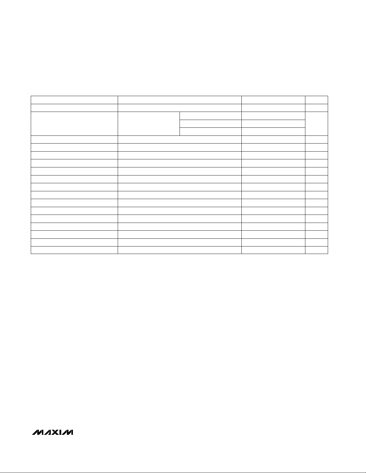
ELECTRICAL CHARACTERISTICS
(VIN= VCC= +5V, FBSEL unconnected, R
TOFF
= 110kΩ, TA= -40°C to +85°C, unless otherwise noted.) (Note 3)
Note 1: Guaranteed by design, not production tested.
Note 2: Idle Mode threshold is defined as the transition point in the load-current range between Idle Mode and constant-off-time
operation.
Note 3: Specifications to -40°C are guaranteed by design, not production tested.
SHDN = GND or V
CC
VIN= 4.5V to 5.5V,
I
LOAD
= 0 to 3A
FBSEL = GND, adjustable output mode, VFB= 1.2V
VCCfalling, 100mV hysteresis
VIN= 4.5V
VIN= 5.5V, VLX= 5.5V or 0
SHDN = GND
VIN= 4.5V
V
FBSEL = GND or REF (Note 1)
I
REF
= 0
Does not include switching losses
CONDITIONS
V0.8
FBSEL = unconnected
SHDN Input Low Voltage
µA-1 1
FBSEL = V
CC
SHDN Input Current
FBSEL = GND or REF
2.2
SHDN Input High Voltage
µs0.85 1.25Off-Time Default Period
µs0.55 4Off-Time Adjustment Range
nA-50 50FB Input Bias Current
V4.0 4.3Undervoltage Lockout Threshold
µA-20 20LX Leakage Current
µA10Shutdown Supply Current
µA600No-Load Supply Current
2.450 2.550
V
3.234 3.366
V4.5 5.5Input Voltage Range
Output Voltage
Ω
0.1NMOS Switch On-Resistance
Ω
0.1PMOS Switch On-Resistance
A3.5 4.75Current-Limit Threshold
1.075 1.110
VV
REF
3.8Output Adjustment Range
V1.075 1.110Reference Output Voltage
UNITSMIN TYP MAXPARAMETER

MAX1623
3A, Low-Voltage, Step-Down Regulator with
Synchronous Rectification and Internal Switches
4 _______________________________________________________________________________________
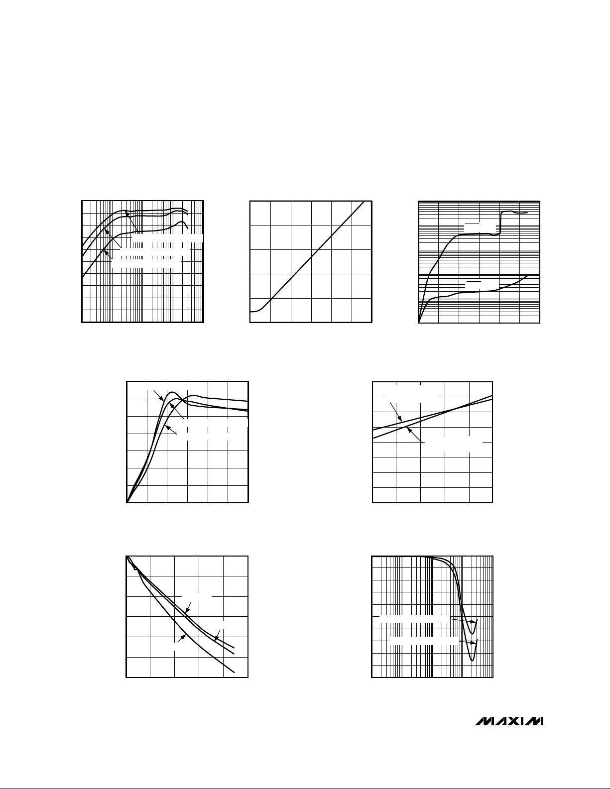
__________________________________________Typical Operating Characteristics
(Circuit of Figure 2, TA = +25°C, unless otherwise noted.)
100
0
0.001 0.1 10.01 10
EFFICIENCY
vs. OUTPUT CURRENT
20
MAX1623 TOC01
OUTPUT CURRENT (A)
EFFICIENCY (%)
40
60
80
90
10
30
50
70
V
OUT
= 3.3V, R
TOFF
= 110kΩ
V
OUT
= 1.1V, R
TOFF
= 280kΩ
V
OUT
= 2.5V, R
TOFF
= 180kΩ
0
1
3
2
4
5
0 200100 300 400 500 600
SWITCH OFF-TIME vs.
OFF-TIME RESISTANCE
MAX1623 TOC02
R
TOFF
(kΩ)
t
OFF
(µs)
1000
100
10
1
0.1
0.01
0123
4
56
SUPPLY CURRENT
vs. INPUT VOLTAGE
MAX1623 TOC03
INPUT VOLTAGE (V)
SUPPLY CURRENT (µA)
SHDN = IN
SHDN = GND
0
150
50
100
250
200
350
300
0 1000 1500500 2000 2500 3000
SWITCHING FREQUENCY
vs. LOAD CURRENT
MAX1623 TOC04
LOAD CURRENT (mA)
SWITCHING FREQUENCY (kHz)
V
OUT
= 2.5V, R
TOFF
= 180kΩ
V
OUT
= 3.3V, R
TOFF
= 110kΩ
V
OUT
= 1.1V, R
TOFF
= 280kΩ
0
200
150
100
50
300
250
350
400
4.5 4.94.7 5.1 5.3 5.5
SWITCHING FREQUENCY
vs. INPUT VOLTAGE
MAX1623 TOC05
INPUT VOLTAGE (V)
SWITCHING FREQUENCY (kHz)
VIN = 5V, V
OUT
= 3.3V,
R
TOFF
= 110kΩ
VIN = 5V, V
OUT
= 2.5V,
R
TOFF
= 180kΩ
0
-0.50
0.10.01 10.001 10
LOAD REGULATION ERROR
vs. LOAD CURRENT
-0.40
MAX1623 TOC07
LOAD CURRENT (A)
LOAD REGULATION ERROR (%)
-0.30
-0.20
-0.10
-0.35
-0.45
-0.25
-0.15
-0.05
V
OUT
= 2.5V, R
TOFF
= 180kΩ
V
OUT
= 3.3V, R
TOFF
= 110kΩ
-0.01
-0.02
-0.03
-0.04
-0.05
-0.06
0
0 5 10 15 20 25
REFERENCE LOAD REGULATION ERROR
vs. REFERENCE LOAD CURRENT
MAX1623 TOC06
REFERENCE LOAD CURRENT (µA)
REFERENCE LOAD REGULATION ERROR (%)
TA = +25°C
T
A
= -40°C
T
A
= +85°C
 Loading...