

________________General Description
The MAX1615/MAX1616 are micropower, SOT23-5 linear regulators that supply always-on, keep-alive power
to CMOS RAM and microcontrollers (µCs) in systems
with high-voltage batteries. Key features include wide
input voltage range, low dropout voltage, and low quiescent supply current.
Despite a miserly 8µA (max) no-load supply current, the
MAX1615/MAX1616 have excellent line-transient
response and AC power-supply rejection ratio. They
provide a clean, fixed 5V or 3.3V output (MAX1615) or
an adjustable 1.24V to 28V output (MAX1616), even
when subjected to fast supply-voltage changes that
occur during the switchover from battery to AC adapter
input power. The space-saving SOT23-5 package has
excellent thermal characteristics and tolerates up to
571mW of power dissipation. Fault protection is provided by internal foldback current limiting and thermalshutdown circuitry.
________________________Applications
CMOS/RTC Backup Power
Microcontroller Power
Notebook Computers
Smart-Battery Packs
PDAs and Handy-Terminals
Battery-Powered Systems
____________________________Features
♦ 4V to 28V Input Range
♦ 8µA (max) Quiescent Supply Current
♦ <1µA Shutdown Supply Current
♦ 3.3V or 5V, Pin-Selectable Output (MAX1615)
Adjustable 1.24V to 28V Output (MAX1616)
♦ 30mA Output Current
♦ ±2% Initial Output Accuracy
♦ Thermal-Overload Protection
♦ 5-Pin SOT23 Package
♦ Low Cost
MAX1615/MAX1616
High-Voltage, Low-Power Linear Regulators
for Notebook Computers
________________________________________________________________
Maxim Integrated Products
1
GND
5/3 (FB)
OUT
( ) ARE FOR MAX1616.
1
5
SHDN
IN
MAX1615
MAX1616
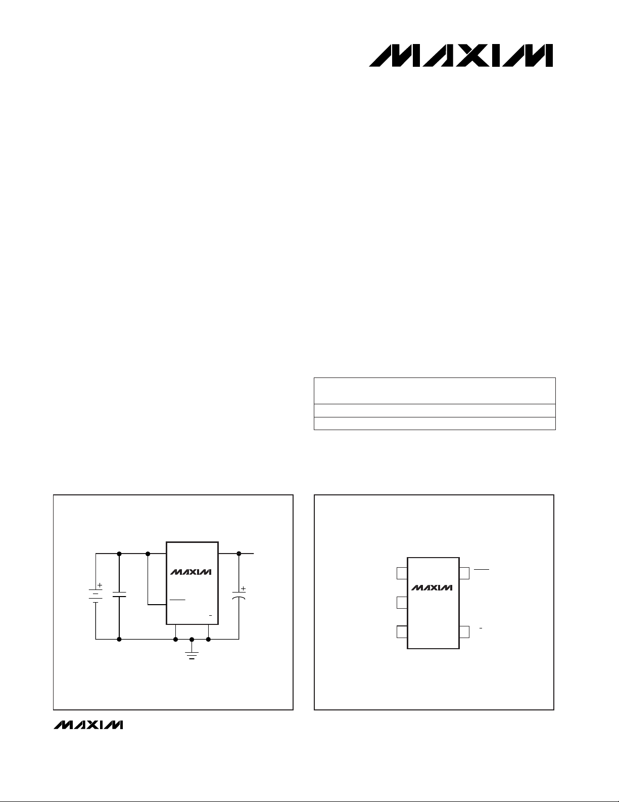
SOT23-5
TOP VIEW
2
3
4
___________________Pin Configuration
IN
OUT
SHDN
GND 5/3
BATTERY
C
IN
0.1µF
C
OUT
4.7µF
OUTPUT
VOLTAGE
MAX1615
____________Typical Operating Circuit
19-1225; Rev 2; 1/98
PART
MAX1615EUK-T
-40°C to +85°C
TEMP. RANGE
PIN-
PACKAGE
5 SOT23-5
_______________Ordering Information
For free samples & the latest literature: http://www.maxim-ic.com, or phone 1-800-998-8800
For small orders, phone 408-737-7600 ext. 3468.
SOT
TOP MARK
ABZD
MAX1616EUK-T
ABZE-40°C to +85°C 5 SOT23-5
V
MAX1615/MAX1616
High-Voltage, Low-Power Linear Regulators
for Notebook Computers
2 _______________________________________________________________________________________
ABSOLUTE MAXIMUM RATINGS
ELECTRICAL CHARACTERISTICS
(VIN= 15V, SHDN = VIN, I
LOAD
= 5µA, TA= T
MIN
to T
MAX
, unless otherwise noted. Typical values are at TA= +25°C.) (Note 2)
Stresses beyond those listed under “Absolute Maximum Ratings” may cause permanent damage to the device. These are stress ratings only, and functional
operation of the device at these or any other conditions beyond those indicated in the operational sections of the specifications is not implied. Exposure to
absolute maximum rating conditions for extended periods may affect device reliability.
IN to GND .................................................................-0.3V to 30V
Terminal Voltages to GND
SHDN to GND...........................................-0.3V to (V
IN
+ 0.3V)
5/3 to GND ............................................-0.3V to (V
OUT
+ 0.3V)
FB (MAX1616) to GND .........................-0.3V to (V
OUT
+ 0.3V)
OUT to GND...........................................................-0.3V to 30V
OUT Short-Circuit to GND ...............................................30sec
Continuous OUT Current.....................................................40mA
Continuous Power Dissipation (T
A
= +70°C) (Note 1)
SOT23-5 (derate 7.1mW/°C above +70°C)...................571mW
Operating Temperature Range
MAX161_EUK-T ...............................................-40°C to +85°C
Storage Temperature Range.............................-65°C to +160°C
Lead Temperature (soldering, 10sec).............................+300°C
Note 1: See
Operating Region and Power Dissipation
section.
FB Input Current (MAX1616) I
FB
-10 12 30 nAVFB= 1.3V
FB Threshold (MAX1616)
(Note 3)
V
FBT
1.215 1.240 1.265
V
FB = OUT,
VIN= 6V to 28V
TA= +25°C,
I
LOAD
= 1mA
1.18 1.28
TA= T
MIN
to T
MAX
,
I
LOAD
= 5µA to 30mA
Output Voltage (MAX1615)
(Note 3)
3.15 3.48
I
LOAD
= 5µA to 30mA,
TA= T
MIN
to T
MAX
,
VIN= 6V to 28V
5/3 = GND
4.75 5.25
5/3 = OUT
4.95 5.05 5.15
5/3 = OUT
3.26 3.33 3.40
I
LOAD
= 1mA,
TA= +25°C,
VIN= 6V to 28V
5/3 = GND
Dropout Supply Current 70 µA
Output set to 5V,
VIN= 4V
TA= +25°C
T
MIN
= T
MIN
to T
MAX
TA= +25°C
Start-Up Overshoot V
OSH
0.5 %V
OUT
RL= 500Ω, C
OUT
= 10µF within 90% of nominal
output voltage
PARAMETER SYMBOL MIN TYP MAX UNITS
Shutdown Supply Current I
IN
3
µA
1.5
Minimum Load Current 5 µA
Input Voltage Range V
IN
4 28 V
6.2 8
Supply Current I
IN
15
µA
Output Current Limit 100 mA
OUT Reverse Leakage
Current
70 µA
Capacitive Load
Requirements (Note 5)
0.16
µF/mA
Start-Up Time Response 1 ms
CONDITIONS
SHDN = GND
(shutdown mode)
VIN= 6V
IN = unconnected, V
OUT
forced to 5V
SHDN = IN, TA= +25°C
MAX1615
SHDN = IN, VIN= 6V to 28V, TA= T
MIN
to T
MAX
Rising edge of IN or SHDN to OUT within specification limits, R
L
= 500Ω, C
OUT
= 6.8µF,
V
OUT
set to 5V
MAX1616 0.23
Dropout Voltage ∆V
DO
350 mVI
LOAD
= 30mA (Note 4)
V
MAX1615/MAX1616
High-Voltage, Low-Power Linear Regulators
for Notebook Computers
_______________________________________________________________________________________ 3
ELECTRICAL CHARACTERISTICS (continued)
(VIN= 15V, SHDN = VIN, I
LOAD
= 5µA, TA= T
MIN
to T
MAX
, unless otherwise noted. Typical values are at TA= +25°C.) (Note 2)
Note 2: Limits are 100% production tested at T
A
= +25°C. Limits over the operating temperature range are guaranteed through
correlation using standard quality-control (SQC) methods.
Note 3: Pulse tested at V
IN
= 28V, I
LOAD
= 30mA to avoid exceeding package power-dissipation limits.
Note 4: Guaranteed by design. Tested with V
OUT
set to 5V. Dropout voltage is tested by reducing the input voltage until V
OUT
drops
to 100mV below its nominal value, measured with V
IN
starting 2V above V
OUT
.
Note 5: Use at least 1µF minimum for light loads. Add 0.125µF/mA (0.2µF/mA for the MAX1616) for loads greater than 100µA,
not production tested. See
Capacitor Selection
in the
Applications Information
section.
60
0
0 30
SAFE LOAD-CURRENT
OPERATING AREA
vs. SUPPLY VOLTAGE
20
10
50
MAX1615-01
SUPPLY VOLTAGE (V)
OUTPUT CURRENT (mA)
105 252015
40
30
POWERDISSIPATION
LIMIT REGION
V
OUT
= 5V
8
0
5 30
GROUND CURRENT
vs. SUPPLY VOLTAGE
AT VARIOUS LOADS
2
3
1
6
7
MAX1615-02
SUPPLY VOLTAGE (V)
GROUND CURRENT (mA)
10 252015
5
4
65mA
55mA
45mA
35mA
15mA
5mA
25mA
9.0
5.0
5 30
SUPPLY CURRENT
vs. SUPPLY VOLTAGE
6.0
6.5
5.5
8.0
8.5
MAX1615-03
SUPPLY VOLTAGE (V)
SUPPLY CURRENT (µA)
25201510
7.5
7.0
TA = +85°C
TA = +25°C
TA = -40°C
__________________________________________Typical Operating Characteristics
(V
OUT
set to 5V, TA = +25°C, unless otherwise noted.)
SHDN Input Threshold
Voltage
CONDITIONS
V
0.25V
IL
UNITSMIN TYP MAXSYMBOLPARAMETER
SHDN Input Current
V
SHDN
= 0V or 15V µA-1 1
Thermal-Shutdown
Temperature
V
SHDN
= 0V or 15V, hysteresis = +20°C °C150T
SHDN
V
IH
1.4

MAX1615/MAX1616
High-Voltage, Low-Power Linear Regulators
for Notebook Computers
4 _______________________________________________________________________________________
100µs/div
LOAD-TRANSIENT RESPONSE
I
OUT
30mA/div
V
OUT
50mV/div
MAX1615-08
____________________________Typical Operating Characteristics (continued)
(V
OUT
set to 5V, TA = +25°C, unless otherwise noted.)
0
10
20
30
40
50
60
70
80
90
4.0 4.2 4.4 4.6 4.8 5.0 5.2 5.4 5.6 5.8 6.0
DROPOUT SUPPLY CURRENT
vs. SUPPLY VOLTAGE
MAX1615-09
SUPPLY VOLTAGE (V)
DROPOUT SUPPLY CURRENT (µA)
TA = +85°C
TA = +25°C
TA = 0°C
TA = -40°C
0
0.05
0.10
0.15
0.20
0.25
0.30
0 5 10 15 20 25 30 35 40
DROPOUT VOLTAGE
vs. LOAD CURRENT
MAX1615-10
LOAD CURRENT (mA)
V
IN
- V
OUT
(V)
50µs/div
LINE-TRANSIENT RESPONSE
+20V
V
OUT
50mV/div
V
IN
C
OUT
4.7µF
C
IN
10µF
MAX1615-07
+10V
500µs/div
TIME TO EXIT SHUTDOWN
+5V
+5V
OUT
0V
SHDN
MAX1615-06
VIN = 10V
0V
1.6
0
4 28
SHUTDOWN SUPPLY CURRENT
vs. SUPPLY VOLTAGE
0.4
0.6
0.2
1.2
1.4
MAX1615-04
SUPPLY VOLTAGE (V)
SHUTDOWN SUPPLY CURRENT (µA)
242016128
1.0
0.8
-70
0
0.01 100
RIPPLE REJECTION vs. FREQUENCY
-20
-30
-10
-50
-60
MAX1615-05
FREQUENCY (kHz)
RIPPLE REJECTION (dB)
1010.1
-40
I
LOAD
= 10mA
_______________Detailed Description
The MAX1615/MAX1616 low-quiescent-current linear
regulators are designed primarily for high input voltage
applications. The MAX1615 supplies a preselected 3.3V
or 5.0V output for loads up to 30mA. The MAX1616
provides an adjustable voltage from 1.24V to 28V. The
maximum output current is a function of the package’s
maximum power dissipation for a given temperature. A
5µA load is required to maintain output regulation.
The MAX1615’s output voltage is fed back through an
internal resistor voltage divider connected to OUT. Set
the output voltage to either 3.3V or 5.0V with the 5/3 pin.
Select the 5V output by connecting 5/3 to OUT, or the
3.3V output by connecting 5/3 to GND.
The MAX1616 uses external feedback, allowing the out-
put voltage to be set by external resistors (see
Setting
the MAX1616 Output Voltage
section). The typical FB
threshold is at 1.24V.
Shutdown
The device enters shutdown mode when SHDN is low.
In shutdown mode, the pass transistor, control circuit,
reference, and all biases turn off, reducing the supply
current to below 1µA. Connect SHDN to IN for automatic
start-up.
Current Limit
Output current is limited to 100mA (typical). The current
limit exceeds the 30mA (max) safe operating limit. The
output can be shorted to ground for 30 seconds without
damaging the part.
Thermal-Overload Protection
When the junction temperature exceeds TJ= +150°C,
the thermal sensor sends a signal to the shutdown
logic, turning off the pass transistor and allowing the IC
to cool. The thermal sensor turns the pass transistor on
again after the IC’s junction temperature cools by
+20°C (typical), resulting in a pulsating output during
continuous thermal-overload conditions.
Operating Region and Power Dissipation
Maximum power dissipation depends on the thermal
resistance of the case and circuit board, the temperature difference between the die junction and ambient
air, and the rate of air flow. The device’s power dissipa-
MAX1615/MAX1616
High-Voltage, Low-Power Linear Regulators
for Notebook Computers
_______________________________________________________________________________________ 5
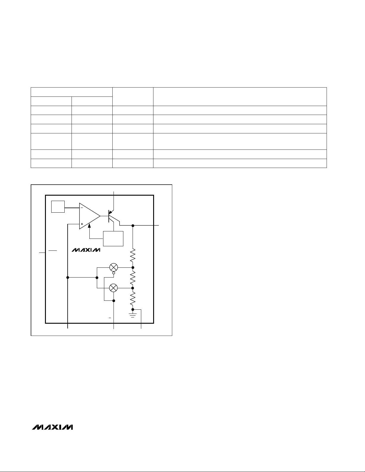
______________________________________________________________Pin Description
1 IN Positive Input Voltage. Connect to a +4V to +28V supply.
2 GND Ground
4
5/3
Preset Output Voltage Select. Connect to GND for 3.3V output or to OUT
for 5.0V output.
5
SHDN
Shutdown, active low input. Connect to IN for automatic start up.
Figure 1. Functional Diagram
1
2
PIN
—
5
NAME FUNCTION
MAX1615 MAX1616
3 OUT Regulator Output3
— FB Feedback Input. Regulates to 1.24V nominally.4
VREF
SHDN
MAX1615
MAX1616
IN
OUT
CURRENT
LIMIT
FB
(MAX1616)
5/3
(MAX1615)
GND

MAX1615/MAX1616
High-Voltage, Low-Power Linear Regulators
for Notebook Computers
6 _______________________________________________________________________________________
___________________Chip Information
TRANSISTOR COUNT: 386
tion is P = I
OUT(VIN
- V
OUT
). The power dissipation at
+70°C ambient is 571mW (see
Absolute Maximum
Ratings
). The thermal resistance junction-to-case of the
SOT23-5 package is 81°C/W, and the maximum safe
junction temperature is +150°C.
The GND pin performs the dual function of providing an
electrical connection to ground and channeling heat
away. Connect GND to ground using a large pad or
ground plane.
__________Applications Information
Setting the MAX1616 Output Voltage
Set the MAX1616’s output voltage with two resistors, R1
and R2 (Figure 2). Choose R2 = 250kΩ to maintain a
5µA minimum load and calculate R1 using the following
equation:
where V
FBT
= 1.24V (typical).
Capacitor Selection
Use a 0.1µF minimum capacitor on the input. Higher
values will improve line-transient response.
Use 1µF minimum on the output, or 4.7µF for the full
30mA load current (6.8µF, MAX1616). Otherwise, use
1µF plus 0.125µF/mA (0.2µF/µA, MAX1616). For output
voltages less than 3.3V, use 15µF instead of 6.8µF. The
output capacitor’s effective series resistance (ESR) must
be less than 1Ω for stable operation.
Output Voltage Noise
The MAX1615/MAX1616 typically exhibit 5mVp-p of
noise during normal operation. This is negligible in
most applications. In applications that include analogto-digital converters (ADCs) of more than 12 bits, consider the ADC’s power-supply-rejection specifications.
Transient Response
The
Typical Operating Characteristics
show the
MAX1615/MAX1616’s load-transient response. Two of
the output response’s components can be observed on
the load-transient graph: a DC shift from the output
impedance due to the different load currents, and the
transient response. Typical step changes in the load
current from 10mA to 20mA produce 50mV transients.
Increasing the output capacitor’s value attenuates transient spikes.
R1 = R2
V
V
OUT
FBT
−
1
Table 1. Surface-Mount Capacitor
Manufacturers
MANUFACTURER CAPACITOR
Sprague 593D, 595 series
Electrolytic
AVX TPS series
TYPE
Matsuo 267 series
Ceramic
AVX X7R
Matsuo X7R
Table 2. Component Suppliers
PHONE FAX
(803) 626-3123
(714) 960-6492
(603) 224-1430
AVX (803) 946-0690
Sprague
SUPPLIER
Matsuo (714) 969-2491
(603) 224-1961
Figure 2. MAX1616 Typical Application Circuit
IN
6V TO
28V
*15µF for V
OUT
0.1µF
SHDN
<3.3V
OUT
MAX1616
FB
GND
OUTPUT
VOLTAGE
R1
6.8µF*
R2

MAX1615/MAX1616
High-Voltage, Low-Power Linear Regulators
for Notebook Computers
_______________________________________________________________________________________ 7
__________________________________________________Tape-and-Reel Information
P
D
E
F
W
P
2
P
0
D
1
A
0
B
0
K
0
t
±0.102
±0.102
A
0
B
0
D
D
1
3.200
3.099
1.499
0.991
±0.102
±0.051
±0.102
±0.102
1.753
3.505
1.397
3.988
E
F
K
0
P
+0.102
+0.000
NOTE: DIMENSIONS ARE IN MM.
AND FOLLOW EIA481-1 STANDARD.
+0.305
-0.102
+0.254
+0.000
P
0
3.988 ±0.102
P
0
10 40.005 ±0.203
P
2
2.007 ±0.051
t 0.254 ±0.127
W 8.001
5 SOT23-5

MAX1615/MAX1616
High-Voltage, Low-Power Linear Regulators
for Notebook Computers
Maxim cannot assume responsibility for use of any circuitry other than circuitry entirely embodied in a Maxim product. No circuit patent licenses are
implied. Maxim reserves the right to change the circuitry and specifications without notice at any time.
8
_____________________Maxim Integrated Products, 120 San Gabriel Drive, Sunnyvale, CA 94086 408-737-7600
© 1998 Maxim Integrated Products Printed USA is a registered trademark of Maxim Integrated Products.
________________________________________________________Package Information
SOT5L.EPS
 Loading...