19-1176; Rev 0; 12/96
High-Side, N-Channel MOSFET
Switch Driver
_______________General Description
The MAX1614 drives high-side, N-channel power MOSFETs
to provide battery power-switching functions in portable
equipment. N-channel power MOSFETs typically have
one-third the on-resistance of P-channel MOSFETs of similar size and cost. An internal micropower regulator and
charge pump generate the high-side drive output voltage,
while requiring no external components.
The MAX1614 also features a 1.5%-accurate low-battery
comparator that can be used to indicate a low-battery
condition, provide an early power-fail warning to the system microprocessor, or disconnect the battery from the
load, preventing deep discharge and battery damage. An
internal latch allows for pushbutton on/off control with very
low current consumption. Off-mode current consumption
is only 6µA while normal operation requires less than
25µA. The MAX1614 is available in the space-saving
µMAX package that occupies about 60% less space than
a standard 8-pin SO.
________________________Applications
Notebook Computers
Portable Equipment
Hand-Held Instruments
Battery Packs
____________________________Features
♦ Internal On/Off Latch
♦ High-Side, N-Channel Power MOSFET Drive
♦ 25µA (max) Quiescent Current
♦ 6µA (max) Off Current
♦ Requires No External Components
♦ 1.5%-Accurate Low-Battery Detector
♦ Space-Saving µMAX Package
♦ 5V to 26V Input Voltage Range
♦ Drives Single or Back-to-Back MOSFETs
♦ Controlled Turn-On for Low Inrush Current
______________Ordering Information
PART
MAX1614C/D
MAX1614EUA -40°C to +85°C
*
Contact factory for dice specifications.
TEMP. RANGE PIN-PACKAGE
0°C to +70°C
Dice*
8 µMAX
MAX1614
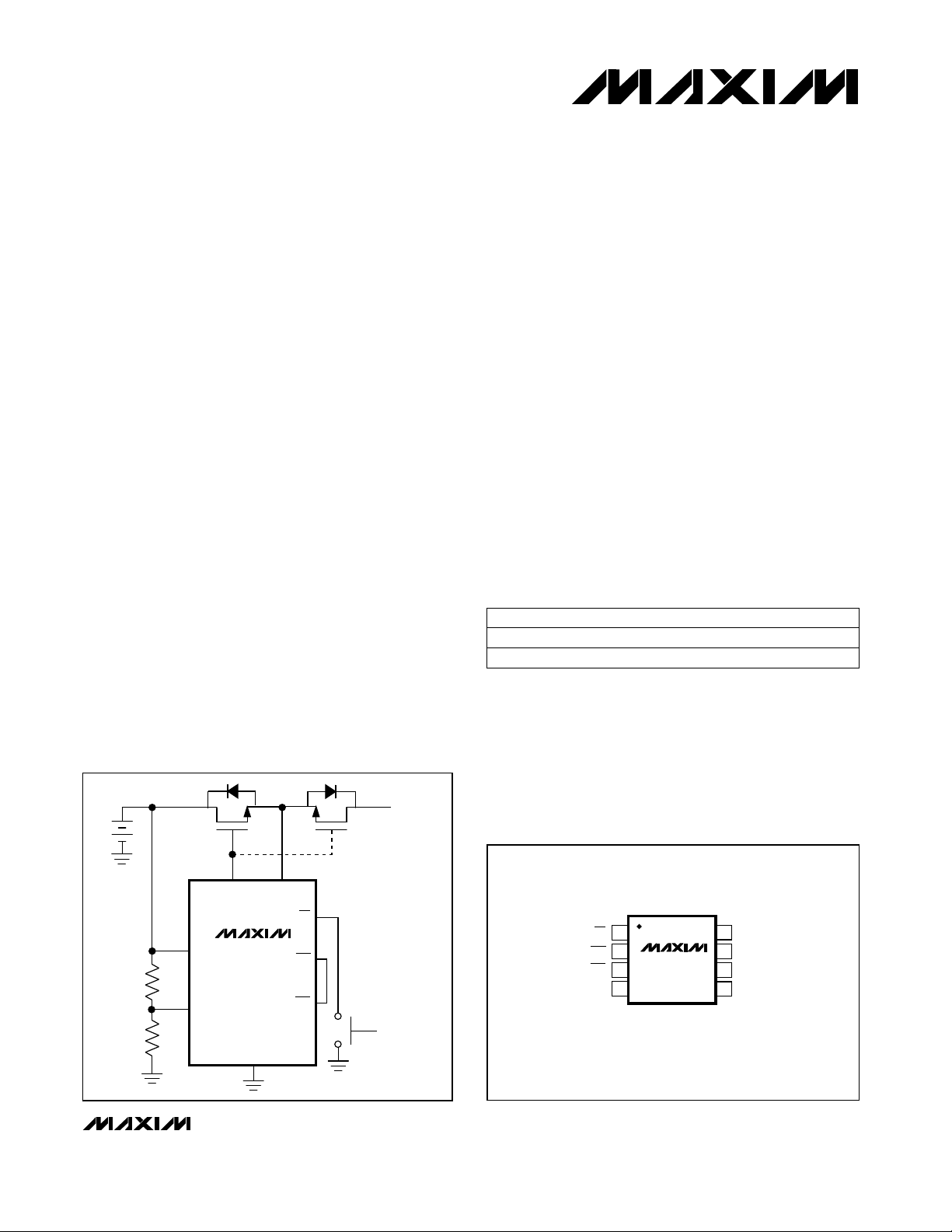
__________Typical Operating Circuit
NN
LOAD
__________________Pin Configuration
OPTIONAL FOR
REVERSE CURRENT
PROTECTION
SRCGATE
ON
MAX1614
BATT
R1
LBI
R2
GND
________________________________________________________________
OFF
LBO
TOP VIEW
ON
OFF
LBO
LBI
1
2
3
4
8
BATT
SRC
MAX1614
µMAX
Maxim Integrated Products
7
GATE
6
5
GND
1
For free samples & the latest literature: http://www.maxim-ic.com, or phone 1-800-998-8800

High-Side, N-Channel MOSFET
OFF
Switch Driver
ABSOLUTE MAXIMUM RATINGS
BATT, SRC to GND.................................................-0.3V to +30V
GATE to SRC..........................................................-0.3V to +12V
GATE to GND.........................................................-0.3V to +36V
GATE + SRC Sink Current, Continuous.............................2.7mA
LBI, LBO, ON, OFF to GND....................................-0.3V to +12V
LBO Current..........................................................................5mA
Stresses beyond those listed under “Absolute Maximum Ratings” may cause permanent damage to the device. These are stress ratings only, and functional
operation of the device at these or any other conditions beyond those indicated in the operational sections of the specifications is not implied. Exposure to
MAX1614
absolute maximum rating conditions for extended periods may affect device reliability.
Continuous Power Dissipation (T
µMAX (derate 4.10mV/°C above +70°C) .....................330mW
Operating Temperature Range ...........................-40°C to +85°C
Junction Temperature......................................................+150°C
Storage Temperature Range.............................-65°C to +160°C
Lead Temperature (soldering, 10sec).............................+300°C
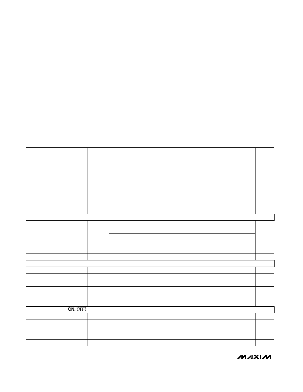
ELECTRICAL CHARACTERISTICS
(V
= 15V, TA= 0°C to +85°C, unless otherwise noted. Typical values are at TA= +25°C.)
BATT
CONDITIONS
V
- V
> 3V, SRC = BATT
SRC
= 26V, ON = OFF = unconnected,
= 1.5V
LBI
= 15V, ON = OFF = unconnected,
= 1.5V,
LBI
= 26V, ON = OFF = unconnected,
= 0A, device latched on, V
LBI
BATT
= 1.5V,
= 15V,
= 0A
= V
= V
SRC
BATT
= 15V
SRC
= 4V, device latched off
LBI
= V
BATT
/ 4
= 5V
= 26V
= 5V
= 5V,
BATT Shutdown Current
Quiescent Current
INTERNAL CHARGE PUMP
GATE Drive Voltage
LOW-BATTERY COMPARATOR
LBI Trip Level
LBI Trip Hysteresis
Minimum V
for Valid LBO
BATT
LBI Input Current
LBO Low Voltage
LBO High Leakage
CONTROL INPUTS (ON,
Input Low Voltage
Input High Voltage
Minimum Input Pulse Width
GATE
V
SHDN
I
BATT
I
SRC
BATT
I
GATE
V
BATT
I
GATE
SRC = BATT
+
V
I
GATE
= 0A, device latched off, V
= 0A, device latched on, V
BATT
SRC = BATT
Measured from GATE to SRC, V
I
V
GS
TH
GATE
Measured from GATE to SRC, V
I
= 1.5µA
GATE
V
GATE
V
GATE
LBI input falling
Tested at V
V
= 1.3V
LBI
OL
OH
LBI
I
SINK
V
LBO
= 1mA
= 11.5V
)
Tested at 2V
Tested at 0.6V
V
V
V
BATT
BATT
BATT
IL
IH
PW
= +70°C)
A
17 30
21 40
6.5 8 9.0
3
TH
UNITSMIN TYP MAXSYMBOLPARAMETER
V526BATT Operating Range
µA47I
µA
µA
V
µA15 60GATE Drive Output Current
mA0.5 2GATE Discharge Current
V1.182 1.20 1.218V
V0.02V
V0.9 4
nA10I
V0.4V
µA0.5V
µA0.5Minimum Input Pull-Up Current
µA1.5 2Maximum Input Pull-Up Current
V0.6V
V2.0V
µs0.5 1.0t
2 _______________________________________________________________________________________

High-Side, N-Channel MOSFET
Switch Driver
ELECTRICAL CHARACTERISTICS
(V
= 15V, TA= -40°C to +85°C, unless otherwise noted.) (Note 1)
BATT
PARAMETER SYMBOL MIN TYP MAX UNITS
BATT Operating Range 5.0 26 V
BATT Shutdown Current
Quiescent Current
INTERNAL CHARGE PUMP
INTERNAL CHARGE PUMP
I
SHDN
I
BATT
I
SAC
V
- V
GATE
V
= 26V, ON = OFF = unconnected,
BATT
= 0A, device latched off, V
I
GATE
+
V
= 26V, ON = OFF = unconnected,
BATT
= 0A, device latched on, V
I
GATE
Measured from GATE to SRC, V
I
= 0A
GATE Drive Voltage V
GS
GATE Drive Output Current 15 60 µA
LOW BATTERY COMPARATOR
LOW-BATTERY COMPARATOR
LBI Trip Level V
TH
GATE
Measured from GATE to SRC, V
I
= 1.5µA, V
GATE
V
= V
GATE
LBI input falling
Note 1: Specifications to -40°C are guaranteed by design and not production tested.
CONDITIONS
> 3V, SRC = BATT
SRC
= 5.25V
SRC
= 15V
SRC
LBI
LBI
BATT
BATT
= 1.5V
= 1.5V
= 15V,
= 5.25V,
8 µA
40
6.5 9.0
3
1.176 1.20 1.224 V
MAX1614
µA
V
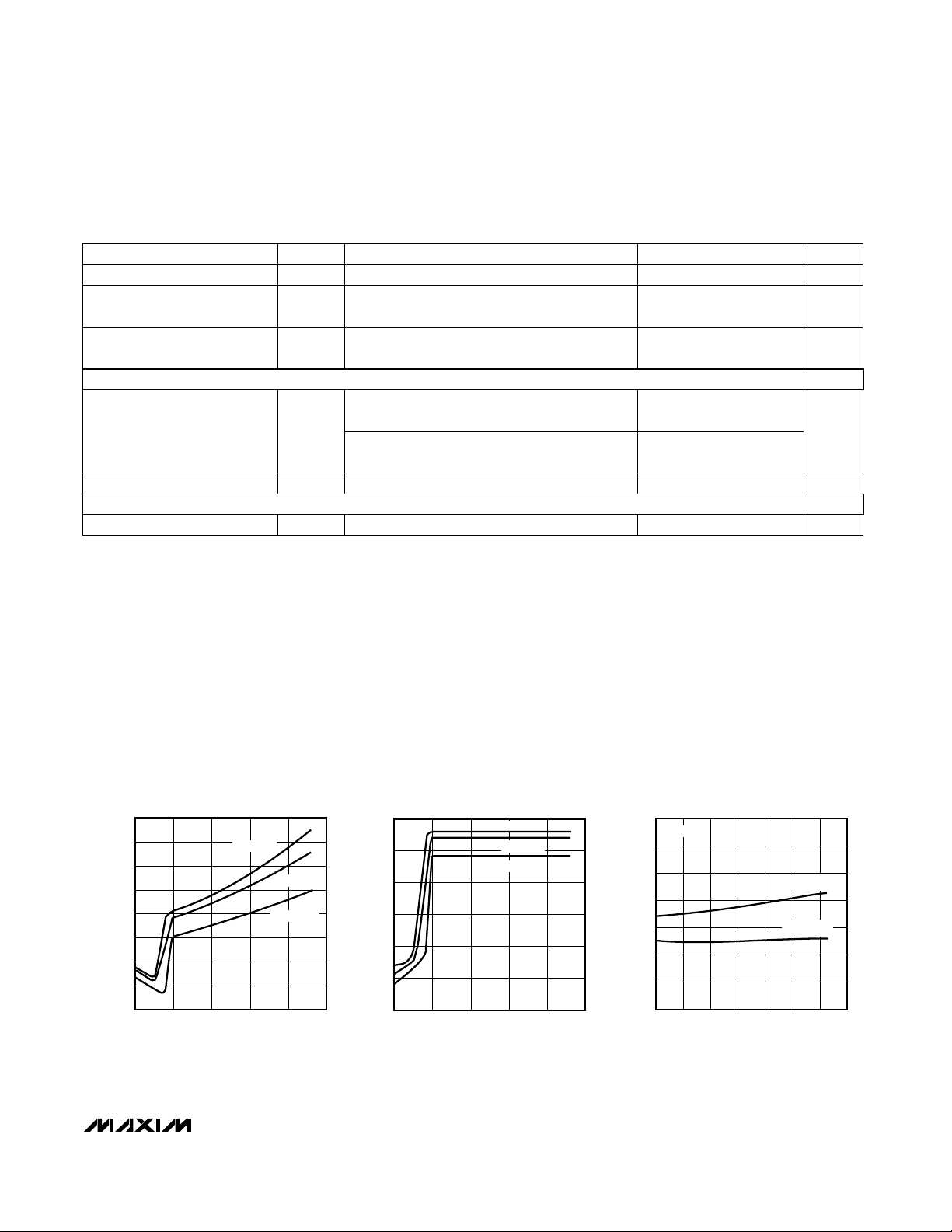
__________________________________________Typical Operating Characteristics
(TA = +25°C, unless otherwise noted.)
ON SUPPLY CURRENT
vs. V
V
BATT
BATT
TA = +85°C
20
(V)
= +25°C
T
A
T
= -40°C
A
25
MAX1614-01
4.0
3.5
3.0
2.5
2.0
SHUTDOWN CURRENT (µA)
1.5
1.0
530
10 15
22
20
18
16
14
12
SUPPLY CURRENT (µA)
10
8
6
530
10 15
_______________________________________________________________________________________ 3
OFF SUPPLY CURRENT
vs. V
BATT
TA = +85°C
TA = +25°C
= -40°C
T
A
20
V
(V)
BATT
1.30
MAX1614-02
1.28
1.26
1.24
1.22
LBI THRESHOLD (V)
1.20
1.18
25
1.16
LOW-BATTERY THRESHOLD
vs. TEMPERATURE
V
= 15V
BATT
V
RISING
LBI
V
FALLING
LBI
-40 100
-20 0
20 60
40
TEMPERATURE (°C)
80
MAX1614-05
 Loading...