

Page 1
For pricing, delivery, and ordering information, please contact Maxim Direct at 1-888-629-4642,
or visit Maxim's website at www.maxim-ic.com.
General Description
The MAX1607 is a current-limited 60mΩ switch with
built-in fault blanking. Its accurate, preset 0.7A to 1.0A
current limit makes it ideal for USB applications. Its low
quiescent supply current (14µA) and standby current
(1µA) conserve battery power in portable applications.
The MAX1607 operates with inputs from +2.7V to
+5.5V, making it ideal for both 3V and 5V systems.
An overcurrent signal (OC) notifies the microprocessor
that the internal current limit has been reached. A 10ms
overcurrent-blanking feature allows momentary faults
(such as those caused when hot-swapping into a
capacitive load) to be ignored, thus preventing false
alarms to the host system. This blanking also prevents
an OC signal from being issued when the device is
powering up.
The MAX1607 has several safety features to ensure that
the USB port is protected. Built-in thermal-overload protection limits power dissipation and junction temperature.
The device also has accurate internal current-limiting
circuitry to protect the input supply against overload.
The MAX1607 is a pin-compatible upgrade to Texas
Instruments’ TPS2014, TPS2015, and TPS2041 for USB
applications. The same die is available in a space-saving 10-pin µMAX®package (MAX1693) and can be
used for next-generation designs. The MAX1694 is similar to the MAX1693, but it has a built-in latch that turns
off the power switch in case of a long-term shortcircuit condition.
The MAX1607 is also offered in a 10-pin TDFN package
(not pin compatible with Texas Instruments TPS2014,
TPS2015, and TPS2041 for USB applications).
Applications
Features
♦ SO Package is Pin Compatible with TPS2014,
TPS2015, and TPS2041
♦ Accurate Current Limit (0.7A min, 1.0A max)
♦ Guaranteed 0.75A Short-Circuit Protection
♦ 10ms Internal OC Blanking Timeout
♦ No Overcurrent (OC) Signal During Power-Up
♦ 125mΩ max High-Side MOSFET
♦ 500mA Continuous Current
♦ Short-Circuit and Thermal Protection with
Overcurrent Logic Output
♦ 1ms Start-Up Time
♦ Undervoltage Lockout
♦ 14µA Quiescent Supply Current
♦ 1µA max Standby Supply Current
♦ +2.7V to +5.5V Supply Range
♦ UL Recognized #E211935
MAX1607
USB Current-Limited Switch
in Pin-Compatible Package
________________________________________________________________ Maxim Integrated Products 1
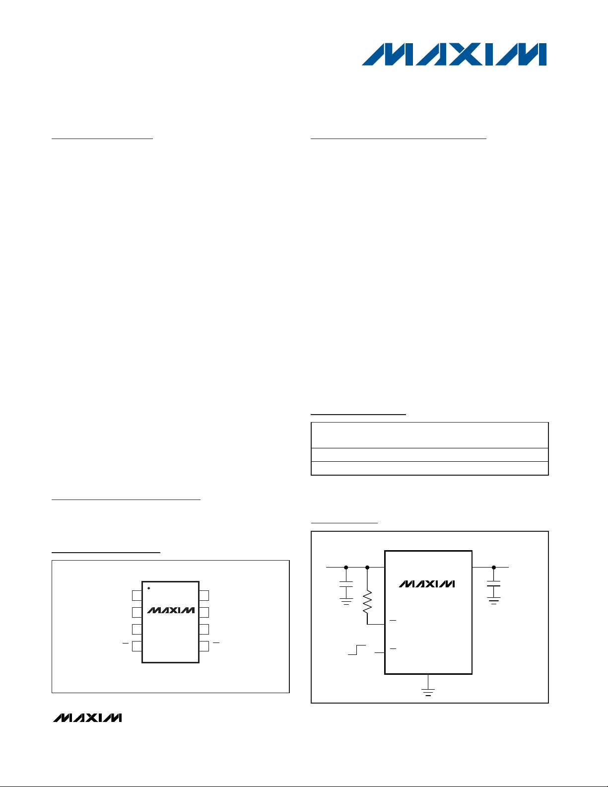
OUT
1
2
87OUT
OUTIN
IN
GND
SO
TOP VIEW
3
4
6
5
MAX1607
OC
EN
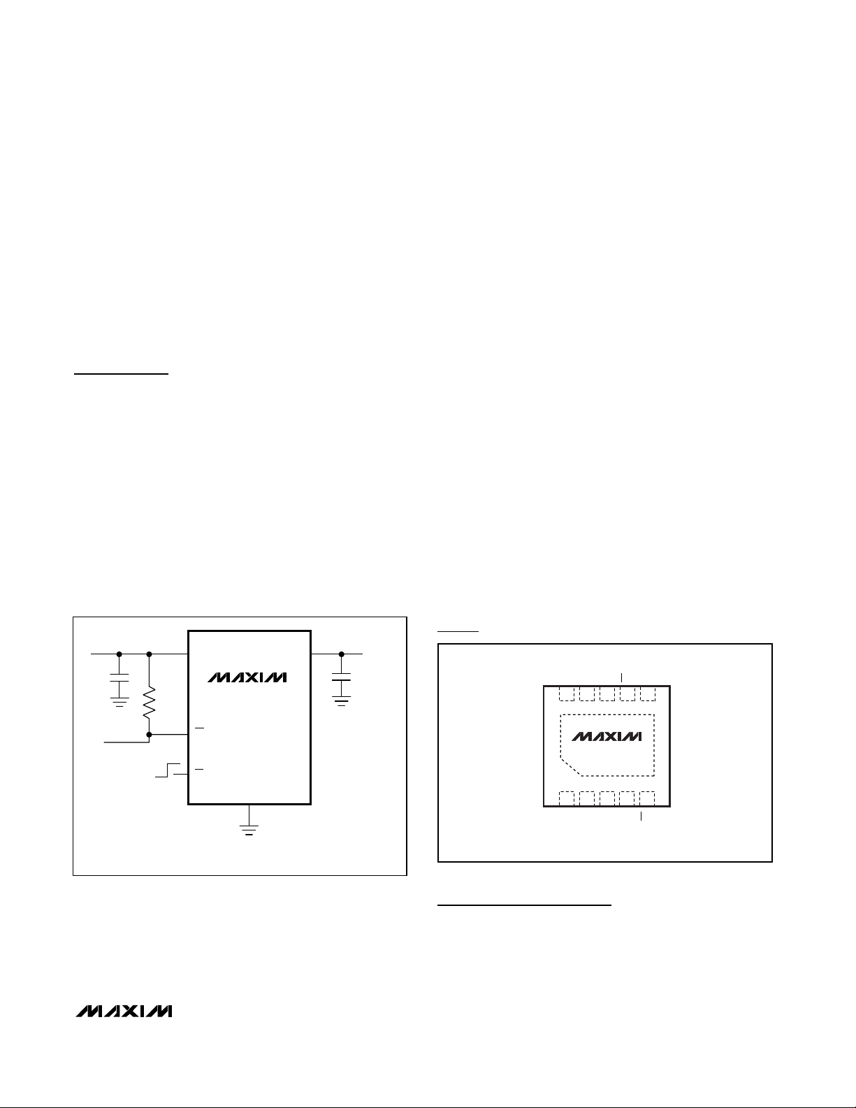
Typical Operating Circuit
19-1544; Rev 2; 09/07
Pin Configurations
Ordering Information
Notebook Computers
USB Ports
USB Hubs
Docking Stations
Pin Configurations continued at end of data sheet.
PART
TEMP RANGE
PINPACKAGE
PKG
CODE
MAX1607ESA
8 SO
S8-5
MAX1607ETB+
T1033-1
*EP = Exposed paddle.
+Denotes a lead-free package.
µMAX is a registered trademark of Maxim Integrated Products, Inc.
-40°C to +85°C
-40°C to +85°C 10 TDFN-EP*
INPUT
+2.7V TO +5.5V
IN OUTPUTOUT
MAX1607
OC
OFF
ON
EN
GND
Page 2
MAX1607
USB Current-Limited Switch
in Pin-Compatible Package
2 _______________________________________________________________________________________
ABSOLUTE MAXIMUM RATINGS
ELECTRICAL CHARACTERISTICS
(VIN= +5V, TA= 0°C to +85°C, unless otherwise noted. Typical values are at TA= +25°C.) (Note 2)
Stresses beyond those listed under “Absolute Maximum Ratings” may cause permanent damage to the device. These are stress ratings only, and functional
operation of the device at these or any other conditions beyond those indicated in the operational sections of the specifications is not implied. Exposure to
absolute maximum rating conditions for extended periods may affect device reliability.
IN, EN, OC to GND .....................................................-0.3 to +6V
OUT to GND ................................................-0.3V to (V
IN
+ 0.3V)
Maximum Switch Current.........................1.2A (internally limited)
OUT Short-Circuit to GND ..........................................Continuous
Continuous Power Dissipation (T
A
= +70°C)
8-Pin SO (derate 5.88mW/°C above +70°C)................471mW
10-Pin TDFN (derate 18.5mW/°C above +70°C) .......1481mW
Operating Temperature Range (extended).........-40°C to +85°C
Storage Temperature Range .............................-65°C to +150°C
Lead Temperature (soldering, 10s) .................................+300°C
TA= 0°C to +85°C
VEN= VIN= 5.5V,
V
OUT
= GND
Timer running
VEN= VIN= V
OUT
= 5.5V
OUT shorted to GND
Force V
OUT
to 4.5V
VIN= 3.7V to 5.5V
VIN= 2.7V to 3.6V
VIN= 5V, C
OUT
= 150µF from EN driven
low to 50% full V
OUT
I
LOAD
= 400mA
TA= +25°C
TA= 0°C to +85°C
VEN= VINor GND
I
LOAD
= 400mA
VIN= 2.7V to 5.5V
CONDITIONS
µA
15
Supply Leakage Current
0.01 2
µA
35
I
Q
Supply Current, High-Level
Input
14 25
µA
0.001 1
Supply Current, Low-Level Input
mA
500 700
I
SC
Short-Circuit Output Current
mA
700 850 1000
I
LIMIT
Overload Output Current
ms
1
Start-Up Time
µA
-1 +1
EN Input Current
V
0.8
V
IL
EN Low-Level Input Voltage
V
2.7 5.5
V
IN
Input Voltage
V
2.4
V
IH
EN High-Level Input Voltage
2.0
µs
3620
t
OFF
Switch Turn-Off Time
60 90
125 mΩ
72 150
R
DS(
ON)
Switch Static Drain-Source
On-State Resistance
µs
80 200
t
ON
Switch Turn-On Time
UNITSMIN TYP MAXSYMBOLPARAMETER
VIN= VOC= 5V
I
SINK
= 1mA, VIN= 3V
Rising edge, 100mV hysteresis
From overcurrent condition to OC assertion
°C
+165
Thermal Shutdown Threshold
ms
71013
t
BL
OC Blanking Timeout Period
µA
1
OC Off-State Current
V
0.4
V
OL
OC Output Low Voltage
V
2.0 2.4 2.6
UVLOUndervoltage Lockout
VIN= 4.4V to 5.5V
VIN= 4.4V to 5.5V
VIN= 3V
Timer not running
VEN= GND, I
OUT
= 0
TA= +25°C
OPERATING CONDITION
POWER SWITCH
ENABLE INPUT (EN)
CURRENT LIMIT
SUPPLY CURRENT
UNDERVOLTAGE LOCKOUT
OVERCURRENT (OC)
THERMAL SHUTDOWN
Page 3
MAX1607
USB Current-Limited Switch
in Pin-Compatible Package
_______________________________________________________________________________________ 3
Note 1: Specifications to -40°C are guaranteed by design, not production tested.
Note 2: TDFN package parts are 100% production tested at T
A
= +25°C. Specifications over operating temperature are guaranteed
by design.
ELECTRICAL CHARACTERISTICS
(VIN= +5V, TA= -40°C to +85°C, unless otherwise noted.) (Note 1)
VIN= VOC= 5V
I
SINK
= 1mA, VIN= 3V
Rising edge, 100mV hysteresis
VEN= V
IN
= 5.5V, V
OUT
= GND
VEN= GND, I
OUT
= 0, timer not running
VEN= VIN= V
OUT
= 5.5V
VIN= 3.0V to 5.5V
VIN= 3.7V to 5.5V
OUT shorted to GND
Force V
OUT
to 4.5V
VIN= 3.0V to 3.6V
VIN= 4.4V to 5.5V
VIN= 3V
I
LOAD
= 400mA
I
LOAD
= 400mA
VEN= VINor GND
CONDITIONS
µA
1
OC Off-State Current
V
0.4
V
OL
OC Output Low Voltage
V
2.0 2.9
UVLOUndervoltage Lockout
µA
15
Supply Leakage Current
µA
25
I
Q
Supply Current, High-Level
Input
µA
2
Supply Current, Low-Level Input
mA
750
I
SC
Short-Circuit Output Current
mA
640 1060
I
LIMIT
Overload Output Current
µA
-1 +1
EN Input Current
V
3.0 5.5
V
IN
Input Voltage
V
0.8
V
IL
EN Low-Level Input Voltage
V
2.4
V
IH
EN High-Level Input Voltage
2.0
125
mΩ
150
R
DS(
ON)
Switch Static Drain-Source
On-State Resistance
µs
200
t
ON
Switch Turn-On Time
µs
120
t
OFF
Switch Turn-Off Time
UNITSMIN TYP MAXSYMBOLPARAMETER
OC Blanking Timeout Period
t
BL
From overcurrent condition to OC assertion
614
ms
OPERATING CONDITION
POWER SWITCH
ENABLE INPUT (EN)
CURRENT LIMIT
SUPPLY CURRENT
UNDERVOLTAGE LOCKOUT
OVERCURRENT (OC)
Page 4

MAX1607
USB Current-Limited Switch
in Pin-Compatible Package
4 _______________________________________________________________________________________
Typical Operating Characteristics
(VIN= +5V, TA = +25°C, unless otherwise noted.)
0
2
4
6
8
10
12
14
16
021 3456
QUIESCENT CURRENT vs. INPUT VOLTAGE
MAX1607-01
INPUT VOLTAGE (V)
QUIESCENT CURRENT (μA)
I
OUT
= 0
VEN = GND
9
11
10
13
12
15
14
16
-40 0 20-20 406080100
QUIESCENT CURRENT vs. TEMPERATURE
MAX1607-02
TEMPERATURE (°C)
QUIESCENT CURRENT (μA)
VIN = 5V
VIN = 3V
100
0.01
OFF SUPPLY CURRENT
vs. TEMPERATURE
0.1
1
10
MAX1607-03
TEMPERATURE (°C)
OFF SUPPLY CURRENT (nA)
-40 0-20 20406080100
VEN = V
IN
0
40
20
80
60
140
120
100
160
-40 0-20 20406080100
TURN-ON TIME vs. TEMPERATURE
MAX1607-07
TEMPERATURE (°C)
t
ON
(μs)
I
LOAD
= 425mA
VIN = 3V
VIN = 5V
0
2
1
4
3
6
5
7
-40 0 20-20 406080100
TURN-OFF TIME vs. TEMPERATURE
MAX1607-08
TEMPERATURE (°C)
t
OFF
(μs)
I
LOAD
= 425mA
VIN = 3V
VIN = 5V
0
2
6
4
10
8
12
-40 0 20-20 406080100
FAULT-BLANKING TIMEOUT
vs. TEMPERATURE
MAX1607-09
TEMPERATURE (°C)
FAULT-BLANKING TIMEOUT (ms)
I
OUT
= 850mA
VIN = 3V OR 5V
100
1000
0.01
-40 0-20 40 10080
OFF SWITCH CURRENT
vs. TEMPERATURE
0.1
1
10
MAX1607-04
TEMPERATURE (°C)
OFF SWITCH CURRENT (nA)
20 60
VEN = V
IN
-40 0-20 40 10080
NORMALIZED ON-RESISTANCE
vs. TEMPERATURE
MAX1607-05
TEMPERATURE (°C)
NORMALIZED R
ON
20 60
0
0.4
0.2
0.8
0.6
1.2
1.0
1.4
I
OUT
= 425mA
0
0.4
0.2
0.8
0.6
1.0
1.2
0231 456
NORMALIZED OUTPUT CURRENT
vs. OUTPUT VOLTAGE
MAX1607-06
OUTPUT VOLTAGE (V)
NORMALIZED OUTPUT CURRENT
SHORT-CIRCUIT CURRENT
I
LIMIT
Page 5
MAX1607
USB Current-Limited Switch
in Pin-Compatible Package
_______________________________________________________________________________________ 5
CH4
CH3
CH1
CH2
2ms/div
MAX1607-10
CURRENT-LIMIT AND OC RESPONSE
CH1 = VIN, 200mV/div, AC-COUPLED
CH2 = V
OUT
, 5V/div
CH3 = V
OC
, 5V/div
CH4 = I
OUT
, 500mA/div
CH4
10μs/div
CH3
CH1
CH2
CURRENT-LIMIT RESPONSE
MAX1607-11
CH1 = VIN, 200mV/div, AC-COUPLED
CH2 = V
OUT
, 5V/div
CH3 = V
OC
, 5V/div
CH4 = I
OUT
, 1A/div
CH4
CH3
CH2
CH1
SWITCH TURN-ON TIME
MAX1607-12
20μs/div
CH1 = V
OUT
, 5V/div
CH2 = V
EN
, 5V/div
CH3 = V
OC
, 5V/div
CH4 = I
OUT
, 200mA/div
CH4
CH3
CH2
CH1
SWITCH TURN-OFF TIME
MAX1607-13
1μs/div
CH1 = V
OUT
, 5V/div
CH2 = V
EN
, 5V/div
CH3 = V
OC
, 5V/div
CH4 = I
OUT
, 200mA/div
START-UP TIME
(TYPICAL USB APPLICATION)
MAX1607-14
V
IN
= 5V, RL = 15Ω, CL = 150μF
CH1 = V
OUT
, 5V/div
CH2 = V
EN
, 5V/div
CH3 = I
IN
, 500mA/div
CH4 = V
OC
, 5V/div
1ms/div
CH2
CH3
CH4
CH1
FULL CURRENT LIMIT CHARGES CAPACITOR
RESISTOR LOAD CURRENT
SHORT-CIRCUIT
CURRENT LIMIT
Typical Operating Characteristics (continued)
(VIN= +5V, TA = +25°C, unless otherwise noted.)
Page 6

MAX1607
USB Current-Limited Switch
in Pin-Compatible Package
6 _______________________________________________________________________________________
Detailed Description
The MAX1607 P-channel MOSFET power switch limits
output current to 0.7A min and 1.0A max. When the output current is increased beyond the current limit (I
LIMIT
),
the current also increases through the replica switch
(I
OUT
/ 6500). The current-limit error amplifier compares
the voltage to the internal 1.24V reference and regulates the current back to the I
LIMIT
(Figure 1).
These switches are not bidirectional; therefore, the
input voltage must be higher than the output voltage.
Continuous Short-Circuit Protection
The MAX1607 is a short-circuit-protected switch. In the
event of an output short-circuit condition, the current
through the switch is foldback-current-limited to 500mA
continuous.
Thermal Shutdown
The MAX1607 has a thermal shutdown feature. The
switch turns off and the OC output goes low immediate-
ly (no overcurrent blanking) when the junction temperature exceeds +165°C. When the MAX1607 cools 20°C,
the switch turns back on. If the fault short-circuit condition is not removed, the switch will cycle on and off,
resulting in a pulsed output.
OC
Indicator
The MAX1607 provides an overcurrent output (OC). A
100kΩ pull-up resistor from OC to IN provides a logic
control signal. This open-drain output goes low when
any of the following conditions occur:
• The input voltage is below the 2.4V undervoltagelockout (UVLO) threshold.
• The die temperature exceeds the thermal shutdown
temperature limit of +165°C.
• The device is in current limit for greater than 10ms.
OC
Blanking
The MAX1607 features 10ms overcurrent blanking.
Blanking allows brief current-limit faults, including
momentary short-circuit faults that occur when hotswapping a capacitive load, and also ensures that no
OC is issued during power-up. When a load transient
causes the device to enter current limit, an internal
Pin Description
MAX1607
P
P
P
OUT
GND
1.24V
N
ON
CURRENT-LIMIT
AMPLIFIER
REPLICA
AMPLIFIER
ON
EN
HOT
IN
CONTROL
CIRCUITRY
OC
10ms
TIMER
Figure 1. Functional Diagram
PIN
SO
NAME FUNCTION
1 6 GND Ground
2, 3
IN
Input. P-channel MOSFET source. Connect all IN pins together and bypass with a 1µF capacitor to
ground.
45 EN Active-Low Switch Enable Input. A logic-low turns on the switch.
57 OC
Overcurrent Indicator Output. This open-drain output goes low when the device is in thermal
shutdown or undervoltage lockout, or during a sustained (> 10ms) current-limit condition.
6, 7, 8
2, 4,
OUT
Switch Output. P-channel MOSFET drain. Connect all OUT pins together and bypass with a 0.1µF
capacitor to ground.
—— EP
Exposed Paddle (TDFN Package Only). Internally connected to GND. Connect to a large ground
plane to maximize thermal performance. Not intended as an electrical connection point.
TDFN
1, 3, 9
8, 10
Page 7
MAX1607
USB Current-Limited Switch
in Pin-Compatible Package
counter starts. If the load fault persists beyond the
10ms overcurrent-blanking timeout, the OC output
asserts low. Ensure that the MAX1607 input is adequately bypassed to prevent input glitches from triggering spurious OC outputs. Input voltage glitches less
than 150mV will not cause a spurious OC output. Loadtransient faults less than 10ms (typ) will not cause an
OC output assertion.
Only current-limit faults are blanked. Die overtemperature faults and input voltage droops below the UVLO
threshold will cause an immediate OC output.
Applications Information
Input Capacitor
To limit the input voltage drop during momentary output
short-circuit conditions, connect a capacitor from IN to
GND. A 1µF ceramic capacitor will be adequate for
most applications; however, higher capacitor values will
further reduce the voltage drop at the input (Figure 2).
Output Capacitor
Connect a 0.1µF capacitor from OUT to GND. This
capacitor helps to prevent inductive parasitics from
pulling OUT negative during turn-off.
Layout and Thermal Dissipation
Important: Optimize the switch response time to output
short-circuit conditions by keeping all traces as short
as possible to reduce the effect of undesirable parasitic
inductance. Place input and output capacitors as close
as possible to the device (no more than 5mm away). All
IN and OUT pins must be connected with short traces
to the power bus. Wide power-bus planes will provide
superior heat dissipation through the MAX1607’s IN
and OUT pins.
Under normal operating conditions, the package can
dissipate and channel heat away. Calculate the maximum power dissipation as follows:
P = (I
LIMIT
)
2
✕
R
ON
where I
LIMIT
is the preset current limit (1.0A max) and
RONis the on-resistance of the switch (125mΩ max).
When the output is short circuited, foldback-current limiting activates and the voltage drop across the switch
equals the input supply. The power dissipated across
the switch increases, as does the die temperature. If
the fault condition is not removed, the thermal-overload-protection circuitry activates (see Thermal
Shutdown section). Wide power-bus planes connected
to IN and OUT and a ground plane in contact with the
device will help dissipate additional heat.
Figure 2. Typical Application Circuit
MAX1607
IN
OUTPUT
OUT
INPUT
1μF
0.1μF
*
*
USB SPECIFICATIONS REQUIRE
A HIGHER VALUE CAPACITOR.
OVERCURRENT
OUTPUT
ON
100k
OFF
GND
OC
EN
Chip Information
TRANSISTOR COUNT: 715
_______________________________________________________________________________________ 7
Pin Configurations (continued)
TOP VIEW
OUTOCGND
OUT
EN
1
2
3
4
5
10
98
7
6
OUT
IN
OUT
IN
IN
MAX1607
+
EP*
*EP = EXPOSED PADDLE
Page 8
MAX1607
USB Current-Limited Switch
in Pin-Compatible Package
8 _______________________________________________________________________________________
SOICN .EPS
PACKAGE OUTLINE, .150" SOIC
1
1
21-0041
B
REV.DOCUMENT CONTROL NO.APPROVAL
PROPRIETARY INFORMATION
TITLE:
TOP VIEW
FRONT VIEW
MAX
0.010
0.069
0.019
0.157
0.010
INCHES
0.150
0.007
E
C
DIM
0.014
0.004
B
A1
MIN
0.053A
0.19
3.80 4.00
0.25
MILLIMETERS
0.10
0.35
1.35
MIN
0.49
0.25
MAX
1.75
0.050
0.016L
0.40 1.27
0.3940.386D
D
MINDIM
D
INCHES
MAX
9.80 10.00
MILLIMETERS
MIN
MAX
16
AC
0.337 0.344 AB8.758.55 14
0.189 0.197 AA5.004.80 8
N MS012
N
SIDE VIEW
H 0.2440.228 5.80 6.20
e 0.050 BSC 1.27 BSC
C
HE
e
B
A1
A
D
0∞-8∞
L
1
VARIATIONS:
Package Information
(The package drawing(s) in this data sheet may not reflect the most current specifications. For the latest package outline information,
go to www.maxim-ic.com/packages
.)
Page 9

MAX1607
USB Current-Limited Switch
in Pin-Compatible Package
_______________________________________________________________________________________ 9
Package Information (continued)
(The package drawing(s) in this data sheet may not reflect the most current specifications. For the latest package outline information,
go to www.maxim-ic.com/packages
.)
6, 8, &10L, DFN THIN.EPS
Page 10
MAX1607
USB Current-Limited Switch
in Pin-Compatible Package
Maxim cannot assume responsibility for use of any circuitry other than circuitry entirely embodied in a Maxim product. No circuit patent licenses are
implied. Maxim reserves the right to change the circuitry and specifications without notice at any time.
10 ____________________Maxim Integrated Products, 120 San Gabriel Drive, Sunnyvale, CA 94086 408-737-7600
© 2007 Maxim Integrated Products is a registered trademark of Maxim Integrated Products, Inc.
Package Information (continued)
(The package drawing(s) in this data sheet may not reflect the most current specifications. For the latest package outline information,
go to www.maxim-ic.com/packages
.)
COMMON DIMENSIONS
SYMBOL MIN. MAX.
A 0.70 0.80
D 2.90 3.10
E 2.90 3.10
A1
0.00 0.05
L 0.20 0.40
PKG. CODE N D2 E2 e JEDEC SPEC b
[(N/2)-1] x e
PACKAGE VARIATIONS
0.25 MIN.k
A2 0.20 REF.
2.00 REF0.25±0.050.50 BSC2.30±0.1010T1033-1
2.40 REF0.20±0.05- - - - 0.40 BSC1.70±0.10 2.30±0.1014T1433-1
1.50±0.10 MO229 / WEED-3
0.40 BSC - - - - 0.20±0.05 2.40 REFT1433-2 14 2.30±0.101.70±0.10
T633-2 6 1.50±0.10 2.30±0.10 0.95 BSC MO229 / WEEA 0.40±0.05 1.90 REF
T833-2 8 1.50±0.10 2.30±0.10 0.65 BSC MO229 / WEEC 0.30±0.05 1.95 REF
T833-3 8 1.50±0.10 2.30±0.10 0.65 BSC MO229 / WEEC 0.30±0.05 1.95 REF
2.30±0.10 MO229 / WEED-3 2.00 REF0.25±0.050.50 BSC1.50±0.1010T1033-2
Revision History
Pages changed at Rev 2: 1, 2, 3, 6, 7–10
 Loading...