

Page 1
19-5720; Rev 0; 12/10
Quad SPST +70V Analog Switches
General Description
The MAX14756/MAX14757/MAX14758 are analog
switches with a low on-resistance of 10I (max) that
conduct equally well in both directions. All devices have
a rail-to-rail analog-signal range. They operate with a single +10V to +70V supply in unipolar applications or Q35V
dual supplies in bipolar applications. The bipolar supplies can be offset and do not have to be symmetrical.
The MAX14756 is a quad normally closed (NC) singlepole/single-throw (SPST) switch, the MAX14757 is a quad
normally open (NO) SPST switch, and the MAX14758 has
two NO and two NC SPST switches. These switches have
5I (typ) on-resistances and low on-leakage currents of
0.01nA (typ). The on-resistance flatness is 0.004I (typ).
The devices are suitable for a multitude of analog signal
routing and switching applications. They are specified
over an extended temperature range of -40NC to +85NC,
but can be operated up to +125NC with elevated leakage
currents.
Applications
Industrial Control Systems
Instrumentation
Battery Management
Environmental Control Systems
Medical Systems
ATE System
Audio Signal Routing/Switching
Automotive
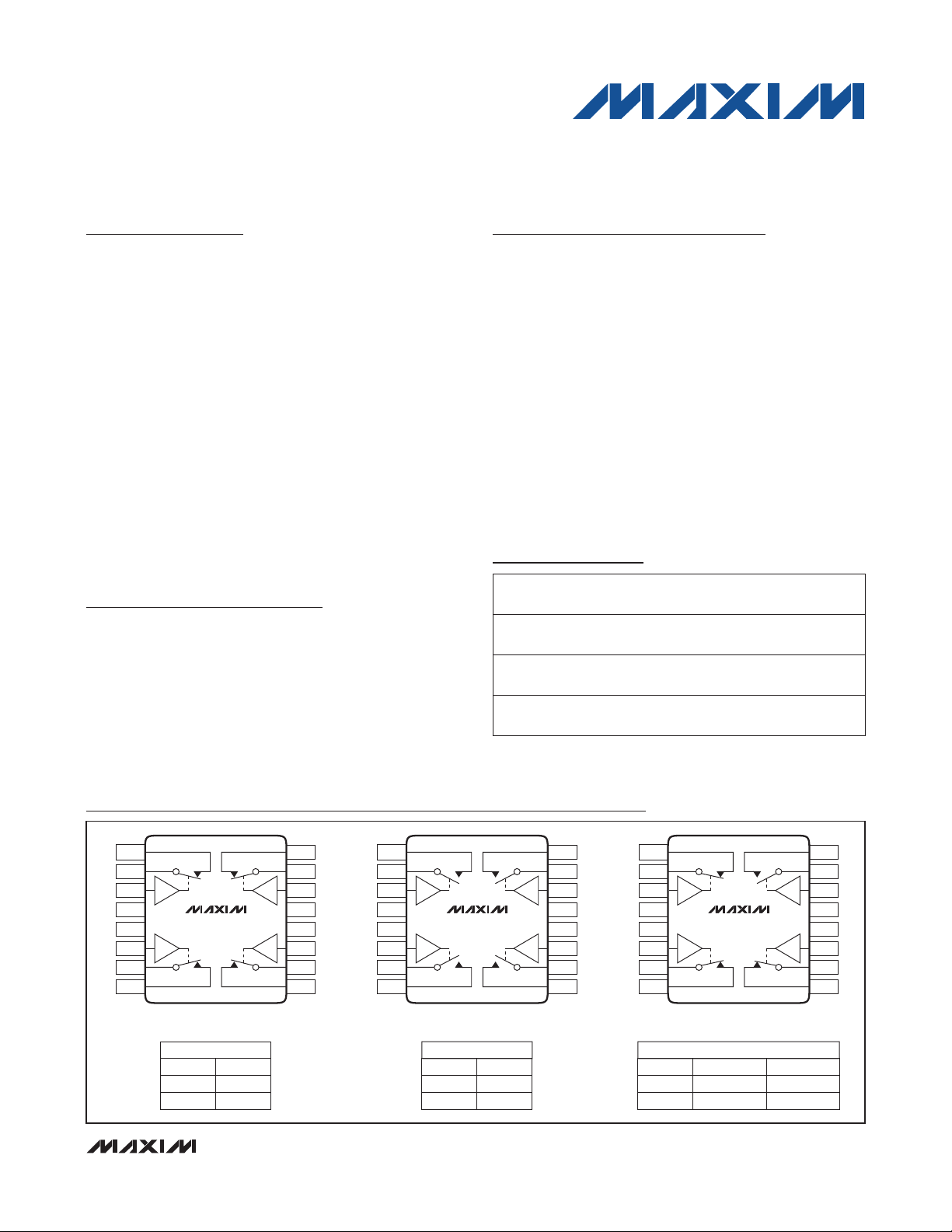
Functional Diagrams
Features
S Single-Supply Operation from +10V to +70V
S Bipolar-Supply Operation Up to ±35V
S On-Resistance of 10I (max)
S R
S 2.5nA (max) Off-Leakage Currents at +85°C
S Overvoltage/Undervoltage Clamping Through
Flatness of 0.004I (typ)
ON
Protection Diodes
S 500µA (typ) Supply Current
S TSSOP 16-Pin Package
S -40°C to +85°C Ambient Temperature Range
S Functionally Compatible to DG411, DG412, and
DG413
S Functionally Operational Up to +125°C
Ordering Information
PART FUNCTION
MAX14756EUE+
MAX14757EUE+
MAX14758EUE+
Quad NC
SPST
Quad NO
SPST
Dual NO +
NC SPST
TEMP
RANGE
-40NC to
+85NC
-40NC to
+85NC
-40NC to
+85NC
+Denotes a lead(Pb)-free/RoHS-compliant package.
PINPACKAGE
16 TSSOP
16 TSSOP
16 TSSOP
MAX14756/MAX14757/MAX14758
V
GND
+
161 A2A1
152 B2B1
143 EN2EN1
V
V
134
SS
MAX14756
TSSOP
MAX14756
EN_ LOGIC SWITCHES
0 CLOSED
1 OPEN
DD
SS
V
125
116 EN3EN4
107 B3B4
98 A3A4
GND
L
+
MAX14757
TSSOP
MAX14757
EN_ LOGIC SWITCHES
0 OPEN
1 CLOSED
+
161 A2A1
152 B2B1
143 EN2EN1
V
V
134
DD
SS
V
125
116 EN3EN4
107 B3B4
98 A3A4
GND
L
EN_ LOGIC SWITCHES 1, 4
0 CLOSED
1 OPEN
MAX14758
TSSOP
MAX14758
SWITCHES 2, 3
OPEN
CLOSED
161 A2A1
152 B2B1
143 EN2EN1
V
134
DD
V
125
L
116 EN3EN4
107 B3B4
98 A3A4
_______________________________________________________________ Maxim Integrated Products 1
For pricing, delivery, and ordering information, please contact Maxim Direct at 1-888-629-4642,
or visit Maxim’s website at www.maxim-ic.com.
Page 2
Quad SPST +70V Analog Switches
ABSOLUTE MAXIMUM RATINGS
VDD to VSS ...........................................................-0.3V to +72V
VSS to GND ..........................................................-36V to +0.3V
VL, EN_ to GND ........-0.3V to the lesser of (+12V, VDD + 0.3V)
A_, B_ to VSS ..............................-0.3V to (VDD + 2V) or 100mA
(whichever occurs first)
Continuous Current into A_, B_ .................................... Q100mA
PACKAGE THERMAL CHARACTERISTICS (Note 1)
TSSOP
Junction-to-Ambient Thermal Resistance (BJA) ...........90NC/W
Junction-to-Case Thermal Resistance (BJC) ................27NC/W
Note 1: Package thermal resistances were obtained using the method described in JEDEC specification JESD51-7, using a four-
layer board. For detailed information on package thermal considerations, refer to www.maxim-ic.com/thermal-tutorial.
Stresses beyond those listed under “Absolute Maximum Ratings” may cause permanent damage to the device. These are stress ratings only, and functional
operation of the device at these or any other conditions beyond those indicated in the operational sections of the specifications is not implied. Exposure to absolute
maximum rating conditions for extended periods may affect device reliability.
ELECTRICAL CHARACTERISTICS—DUAL SUPPLIES
(VDD = +35V, VSS = -35V, V
PARAMETER SYMBOL CONDITIONS MIN TYP MAX UNITS
POWER SUPPLY
VDD Supply-Voltage Range V
VSS Supply-Voltage Range V
VL Logic Supply-Voltage Range V
VDD Supply Current
MAX14756/MAX14757/MAX14758
VSS Supply Current
VL Current I
SWITCH
Analog-Signal Range V
Current Through Switch I
On-Resistance R
On-Resistance Matching
Between Channels
On-Resistance Flatness R
On-Leakage Current I
Off-Leakage Current I
= 0V, VL = +3.3V, TA = -40NC to +85NC, unless otherwise noted. Typical values are at TA = +25NC.)
GND
DD
SS
L
I
DD(OFF)VEN_
I
DD(ON)VEN_
I
SS(OFF)VEN_
I
SS(ON)VEN_
L
A_, VB_
A_, IB_VA_
ON
DR
ON
FLAT(ON)
A/B_(ON)
to switch off state, VA_, V
to switch on state, VA_, V
to switch off state, VA_, V
to switch on state, VA_, V
VL = +11V, V
(0.25 x VL) or ( 0.75 x VL)
Figure 1 V
, V
= +20V -50 +50 mA
B_
IA_, I
= 10mA, VA_, V
B_
IA_, I
= 10mA, VA_, V
B_
(Note 2)
IA_, I
= 10mA, VA_, V
B_
V
= Q20V, VA_= unconnected, Figure 2
B_
V
= Q20V, VA_ = unconnected,
B_
TA = +25NC, Figure 2
V
= Q20V, V
B_
A/B_(OFF)
V
= Q20V, VA_ = -20V, TA = +25NC,
B_
Figure 3
Continuous Power Dissipation (TA = +70NC)
TSSOP (derate 11.1mW/NC above +70NC) .................889mW
Operating Temperature Range .......................... -40NC to +85NC
Storage Temperature Range ............................ -65NC to +150NC
Junction Temperature ................................................... +150NC
Lead Temperature (soldering, 10s) ................................+300NC
Soldering Temperature (reflow) ......................................+260NC
+10 +35 V
-10 -35 V
+1.6 +11 V
= +20V 200 450
B_
= +20V 500 800
B_
= +20V 200 450
B_
= +20V 500 800
B_
EN1
= V
= V
EN2
EN3
= Q20V, Figure 1
B_
= Q20V, 0V
B_
= Q20V
B_
= V
EN4
=
SS
5 10
0.3 0.5
0.004
0.4 mA
V
DD
-5 +5
0.01
= -20V, Figure 3
A_
-2.5 +2.5
0.01
FA
FA
V
I
I
I
nA
nA
2 ______________________________________________________________________________________
Page 3
Quad SPST +70V Analog Switches
ELECTRICAL CHARACTERISTICS—DUAL SUPPLIES (continued)
(VDD = +35V, VSS = -35V, V
PARAMETER SYMBOL CONDITIONS MIN TYP MAX UNITS
LOGIC (EN1, EN2, EN3, EN4)
Input-Voltage Low V
Input-Voltage High V
Input Leakage Current V
DYNAMIC CHARACTERISTICS
VDD/VSS Power-On Time
Enable Turn-On Time t
Enable Turn-Off Time t
Off-Isolation V
Crosstalk V
-3dB Bandwidth BW
Total Harmonic Distortion Plus
Noise
Charge Injection Q A_, B_ = GND, CL = 1nF, Figure 8 580 pC
Switch-On Capacitance C
Switch-Off Capacitance C
= 0V, VL = +3.3V, TA = -40NC to +85NC, unless otherwise noted. Typical values are at TA = +25NC.)
GND
IL
IH
ON
OFF
ISO
CT
THD+N
IN
IN
= 0V or V
EN_
RL = 10kI
V
, VB_= Q10V, RL = 10kI, Figure 4
A _
VA_, VB_= Q10V, RL = 10kI, Figure 4
VA_, VB_= 1V RMS, f = 100kHz, RL = 1kI,
CL = 15pF, Figure 5
RS = RL = 1kI, Figure 6
RS = 50I, RL = 1kI, Figure 7
RS = RL = 1kI, f = 20Hz to 20kHz
VDD = +50V, VSS = 0V, V
f = 1MHz
VDD = +50V, VSS = 0V, V
f = 1MHz
L
, VB_= +4V,
A_
, VB_= +4V,
A _
0.75 x
V
L
-1 +1
145 MHz
0.001 %
0.25 x
V
L
1
35 60
2 3
65 dB
96 dB
40 pF
35 pF
MAX14756/MAX14757/MAX14758
V
V
FA
Fs
Fs
Fs
DC ELECTRICAL CHARACTERISTICS—SINGLE SUPPLY
(VDD = +70V, VSS = V
PARAMETER SYMBOL CONDITIONS MIN TYP MAX UNITS
POWER SUPPLY
VDD Supply-Voltage Range V
SWITCH
On-Resistance R
On-Resistance Matching
Between Channels
Off-Leakage Current I
Note 2: Guaranteed by design; not production tested.
Note 3: All parameters in single-supply operation are expected to be the same as in dual-supply operation.
= 0V, VL = +3.3V, TA = -40NC to +85NC, unless otherwise noted. Typical values are at TA = +25NC.) (Note 2)
GND
DD
ON
DR
A/B_(OFF)VB_
_______________________________________________________________________________________ 3
IA_ = 10mA, VA_, VB_= +20V, Figure 1 5 10
IA_, I
ON
= 10mA, VA_, V
B_
(Note 2)
= +40V, VA_= +10V, Figure 3 -2.5 +2.5 nA
= +70V, 0V
B_
+10 +70 V
0.3 0.5
I
I
Page 4

Quad SPST +70V Analog Switches
Test Circuits/Timing Diagrams
V
V
L
V
L
A_ B_
V
IN
GND
V
V
MAX14756
MAX14757
MAX14758
1µF
DD
1µF1µF
DD
SWITCH
EN_
CLOSED
UNCONNECTED
I
V
SS
V
SS
IN
V
L
V
L
A_ B_
Figure 1. On-Resistance Measurement Figure 2. On-Leakage Current
V
L
V
L
MAX14756/MAX14757/MAX14758
SWITCH
I
A_(OFF)
V
IN
EN_
OPEN
A_ B_
A
GND
V
V
MAX14756
MAX14757
MAX14758
DD
1µF1µF
DD
I
B_(OFF)
A
V
SS
GND
V
OUT
V
V
MAX14756
MAX14757
MAX14758
1µF
DD
1µF1µF
DD
SWITCH
EN_
CLOSED
I
B_(ON)
A
V
OUT
V
SS
V
SS
1µF
V
SS
Figure 3. Off-Leakage Current
4 ______________________________________________________________________________________
Page 5

Quad SPST +70V Analog Switches
Test Circuits/Timing Diagrams (continued)
MAX14756/MAX14757/MAX14758
Figure 4. Enable Switching Time
V
V
MAX14756
MAX14757
MAX14758
1µF
DD
DD
R
S
= 50Ω
V
L
V
L
V
IN
A_
GND
V
L
V
L
GND
1µF1µF
EN_
V
SS
V
SS
V
V
MAX14756
MAX14757
MAX14758
1µF
SWITCH
OPEN
B_
RL = 1kΩ CL = 15pF
DD
1µF1µF
+5V
50%
t
ON
90%
V
L
V
L
A1 EN1
A2
GND
V
V
MAX14756
MAX14757
MAX14758
1µF
DD
DD
V
V
EN_
0V
OUT
0V
50Ω
IN
DD
A_ +10V
B_EN_
V
SS
V
SS
V
OUT
10kΩ50Ω
V
OUT
t
< 20ns
R
< 20ns
t
F
t
OFF
10%
1µF1µF
SWITCH 2 CLOSED
EN2
B2
V
SS
V
SS
V
OUT
RL = 1kΩ
V
OFF-ISOLATION = 20log
OUT
V
IN
Figure 5. Off-Isolation Figure 6. Crosstalk
_______________________________________________________________________________________ 5
CROSSTALK = 20log
V
OUT
V
IN
Page 6

Quad SPST +70V Analog Switches
Test Circuits/Timing Diagrams (continued)
V
V
MAX14756
MAX14757
MAX14758
1µF
DD
1µF1µF
NETWORK
DD
A_
B_
V
SS
V
SS
ON-LOSS = 20log
V
IN
V
OUT
V
OUT
V
IN
ANALYZER
MEAS REF
SWITCH
CLOSED
EN_
V
V
L
L
GND
Figure 7. Frequency Response
V
L
V
L
A_
EN_
MAX14756/MAX14757/MAX14758
50Ω
GND
V
V
MAX14756
MAX14757
MAX14758
1µF
DD
1µF1µF
+5V
V
EN
DD
B_
V
SS
V
SS
V
OUT
CL = 1nF
0V
V
OUT
0V
V
IS THE MEASURED VOLTAGE DUE TO CHARGE
OUT
TRANSFER ERROR Q WHEN THE CHANNEL TURNS OFF.
× V
Q = C
L
OUT
ON ONOFF
V
OUT
Figure 8. Charge Injection
6 ______________________________________________________________________________________
Page 7

Quad SPST +70V Analog Switches
Typical Operating Characteristics
(TA = +25NC, VL = +3.3V, unless otherwise noted.)
MAX14756/MAX14757/MAX14758
ON-RESISTANCE vs. V
B_
(DUAL SUPPLIES)
4.3
4.2
±35V
(Ω)
4.1
ON
R
4.0
3.9
-35 35
±10V
-5-10-15-20-25-30
V
OUT
±20V
0
(V)
ON-RESISTANCE vs. VB_ AND TEMPERATURE
(SINGLE SUPPLY)
10
VDD = +70V
= 0V
V
SS
8
6
(Ω)
ON
R
4
TA = +85°C
TA = +25°C
2
0
0 70
V
OUT
TA = +125°C
TA = -40°C
(V)
±30V
ON-RESISTANCE vs. VB_ AND TEMPERATURE
(DUAL SUPPLIES)
10
VDD = +35V
= -35V
V
MAX14756 toc01
SS
8
6
(Ω)
ON
R
4
TA = +85°C
TA = +125°C
MAX14756 toc02
4.5
4.4
4.3
(Ω)
ON
R
4.2
ON-RESISTANCE vs. V
(SINGLE SUPPLY)
B_
MAX14756 toc03
+70V
2
TA = +25°C
TA = -40°C
0
30252015105
-35 35
0
-5-10-15-20-25-30
V
(V)
OUT
30252015105
ON-LEAKAGE vs. TEMPERATURE
100
VDD = +35V
= -35V
V
SS
10
MAX14756 toc04
1
I
(ON)
0.1
LEAKAGE CURRENT (nA)
0.01
0.001
6560555045403530252015105
-40 125
TEMPERATURE (°C)
1109580655035205-10-25
4.1
4.0
100
MAX14756 toc05
10
1
0.1
LEAKAGE CURRENT (nA)
0.01
0.001
+20V
0 70
ON-LEAKAGE vs. TEMPERATURE
VDD = +35V
= -35V
V
SS
I
B_(OFF)
-40 125
+40V
V
(V)
OUT
I
A_(OFF)
TEMPERATURE (°C)
605040302010
MAX14756 toc06
1109580655035205-10-25
CHARGE INJECTION vs. TEMPERATURE
1000
VDD = +35V
= -35V
V
SS
800
600
Q (pC)
400
200
0
-40 125
TEMPERATURE (°C)
_______________________________________________________________________________________ 7
SUPPLY CURRENT vs. TEMPERATURE
MAX14756 toc08
(µA)
L
I
100
1000
VDD = +35V
= -35V
V
SS
900
= +3.3V
V
MAX14756 toc07
1109580655035205-10-25
L
800
(µA)
SS
700
, I
DD
I
600
500
400
-40 125
TEMPERATURE (C)
I
DD
I
SS
1109580655035205-10-25
VL INPUT CURRENT vs. V
VDD = +35V
90
= -35V
V
SS
80
70
60
50
40
30
20
10
0
0 5
V
(V)
EN_
EN_
MAX14756 toc09
4321
Page 8

Quad SPST +70V Analog Switches
Typical Operating Characteristics (continued)
(TA = +25NC, VL = +3.3V, unless otherwise noted.)
CROSSTALK vs. FREQUENCY
0
VDD = +35V
= -35V
V
SS
-20
-40
-60
CROSSTALK (dB)
-80
-100
0.01 1000
FREQUENCY (MHz)
MAX14756 toc10
OFF-ISOLATION (dB)
1001010.1
OFF-ISOLATION vs. FREQUENCY
0
VDD = +35V
= -35V
V
SS
-20
-40
-60
-80
-100
-120
0.01 1000
FREQUENCY (MHz)
1001010.1
TOTAL HARMONIC DISTORTION PLUS
NOISE vs. FREQUENCY
0.005
VDD = +35V
= -35V
V
SS
0.004
0.003
THD+N (%)
0.002
MAX14756/MAX14757/MAX14758
0.001
MAX14756 toc13
0
-20
-40
PSRR (dB)
-60
-80
VDD = +35V
= -35V
V
SS
0
MAX14756 toc11
-10
-20
-30
ON-LOSS (dB)
-40
VDD = +35V
V
= -35V
SS
-50
0.01 1000
PSRR vs. FREQUENCY
V
SS
V
DD
ON-LOSS vs. FREQUENCY
MAX14756 toc12
1001010.1
FREQUENCY (MHz)
MAX14756 toc14
0
0.01 100
FREQUENCY (kHz)
TURN-ON TIME vs. INPUT VOLTAGE
50
VDD = +35V
= -35V
V
SS
40
30
(µs)
ON
t
20
10
0
-35 35
0
-5-10-15-20-25-30
VA_ (V)
1010.1
MAX14756 toc15
30252015105
-100
0.01 1000
FREQUENCY (MHz)
TURN-OFF TIME vs. INPUT VOLTAGE
20
VDD = +35V
= -35V
V
SS
15
(µs)
10
OFF
t
5
0
-35 35
-5-10-15-20-25-30
VA_ (V)
0
1001010.1
8 ______________________________________________________________________________________
MAX14756 toc16
30252015105
Page 9

Quad SPST +70V Analog Switches
Pin Configuration
TOP VIEW
+
V
GND
SS
MAX14756
MAX14757
MAX14758
TSSOP
Pin Description
PIN NAME FUNCTION
1 A1 Terminal A of Switch 1
2 B1 Terminal B of Switch 1
3 EN1
4 V
5 GND Ground
6 EN4
7 B4 Terminal B of Switch 4
8 A4 Terminal A of Switch 4
9 A3 Terminal A of Switch 3
10 B3 Terminal B of Switch 3
11 EN3
12 V
13 V
14 EN2
15 B2 Terminal B of Switch 2
16 A2 Terminal A of Switch 2
Enable Input of Switch 1. When EN1 is driven high, the switch’s state (NO/NC) changes (see Tables 1, 2,
and 3).
Negative Supply Voltage. Bypass VSS to GND with a 1FF ceramic capacitor (100V rated) as close as
SS
possible to the pin.
Enable Input of Switch 4. When EN4 is driven high, the switch’s state (NO/NC) changes (see Tables 1, 2,
and 3).
Enable Input of Switch 3. When EN3 is driven high, the switch’s state (NO/NC) changes (see Tables 1, 2,
and 3).
Logic Supply Voltage. Bypass VL to GND with a 1FF ceramic capacitor as close as possible to the pin.
L
Positive Supply Voltage. Bypass VDD to GND with a 1FF ceramic capacitor (100V rated) as close as
DD
possible to the pin.
Enable Input of Switch 2. When EN2 is driven high, the switch’s state (NO/NC) changes (see Tables 1, 2,
and 3).
161 A2A1
152 B2B1
143 EN2EN1
V
134
DD
V
125
L
116 EN3EN4
107 B3B4
98 A3A4
MAX14756/MAX14757/MAX14758
_______________________________________________________________________________________ 9
Page 10

Quad SPST +70V Analog Switches
Detailed Description
The MAX14756/MAX14757/MAX14758 are analog
switches with low on-resistance of 10I (max) that conduct equally well in both directions. All devices have
a rail-to-rail analog-signal range. They operate with a
single +70V supply in unipolar applications or Q35V dual
supplies in bipolar applications. The bipolar supplies
can be offset and do not have to be symmetrical.
The MAX14756 is a quad NC SPST switch, the MAX14757
is a quad NO SPST switch, and the MAX14758 has two
NO and two NC SPST switches. These switches have 5I
Table 1. MAX14756 Truth Table
LOGIC SWITCH
EN1 0 A1/B1 Closed
EN2 0 A2/B2 Closed
EN3 0 A3/B3 Closed
EN4 0 A4/B4 Closed
EN1 1 A1/B1 Open
EN2 1 A2/B2 Open
EN3 1 A3/B3 Open
EN4 1 A4/B4 Open
(typ) on-resistances and low on-leakage currents of 5nA
(max). The on-resistance flatness is 0.004I (typ). These
devices are suitable for a multitude of analog-signal routing and switching applications, and are functonally operational up to +125°C with increased leakage currents.
Applications Information
Low-Distortion Audio
The MAX14756/MAX14757/MAX14758 switches, having
low RON and very low RON variation with signal amplitude, are well suited for low-distortion audio applications. The Typical Operating Characteristics show Total
Table 2. MAX14757 Truth Table
LOGIC SWITCH
EN1 0 A1/B1 Open
EN2 0 A2/B2 Open
EN3 0 A3/B3 Open
EN4 0 A4/B4 Open
EN1 1 A1/B1 Closed
EN2 1 A2/B2 Closed
EN3 1 A3/B3 Closed
EN4 1 A4/B4 Closed
Harmonic Distortion (THD) vs. Frequency graphs for
several signal amplitudes.
Current Through the Switches
The current flowing through every switch must be limited
to Q50mA for normal operation. If the current exceeds
MAX14756/MAX14757/MAX14758
this limit, an internal leakage current flows from the
switch to VSS. Larger input currents do not destroy the
device, as long as the Absolute Maximum Ratings are
not exceeded.
Input-Voltage Clamping
For applications that require input voltages beyond the
supplies rails, the internal input diodes to VDD and VSS
Table 3. MAX14758 Truth Table
LOGIC SWITCH
EN1 0 A1/B1 Closed
EN2 0 A2/B2 Open
EN3 0 A3/B3 Open
EN4 0 A4/B4 Closed
EN1 1 A1/B1 Open
EN2 1 A2/B2 Closed
EN3 1 A3/B3 Closed
EN4 1 A4/B4 Open
can be used to limit the input voltages. As shown in
Figure 9, series resistors can be employed at the inputs
to limit the currents flowing into the diodes during undervoltage and overvoltage conditions. Choose the limiting resistors such that the input currents are limited to
I
(MAX) = 100mA. The values of the current-limit resis-
IN_
tors can be calculated as the larger of R
V (MAX) V
R
LIM
R
LIM
IN DD
=
+
V V (MIN)
SS IN
=
−
−
I (MAX)
IN_
−
I (MAX)
IN_
LIM+
and R
LIM-
During an undervoltage or overvoltage condition, the
input impedance is equal to R
dissipation due to the fault currents needs to be calculated. During an overvoltage or undervoltage clamping
condition on one switch input, the other switches of the
.
MAX14756/MAX14757/MAX14758 operate normally.
If input voltages are expected to go beyond the supply
voltages, but within the absolute maximum supply voltages of the MAX14756/MAX14757/MAX14758, add two
diodes in series with the supplies as shown in Figure 10.
. The additional power
LIM
Beyond-the-Rail Input
10 _____________________________________________________________________________________
Page 11

Quad SPST +70V Analog Switches
R
LIM
V
IN
V
IN
V
IN
V
IN
Figure 9. Input Overvoltage and Undervoltage Clamping
A1
R
LIM
A2
R
LIM
A3
R
LIM
A4
MAX14756/MAX14757/MAX14758
V
DD
MAX14756
MAX14757
MAX14758
V
SS
B1
B2
B3
B4
V+
V
DD
R
A_
V
IN
V
SS
V-
Figure 10. Beyond-the-Rail Application
During undervoltage and overvoltage events, the internal
diodes pull VDD/VSS supplies up/down. An advantage
of this scheme is that the input impedance is high and
currents do not flow though the MAX14756/MAX14757/
MAX14758 during overvoltage and undervoltage events.
The input voltages must be limited to the voltages specified in the Absolute Maximum Ratings section.
Chip Information
B_
PROCESS: BiCMOS
Package Information
For the latest package outline information and land patterns
(footprints), go to www.maxim-ic.com/packages. Note that a
“+”, “#”, or “-” in the package code indicates RoHS status only.
Package drawings may show a different suffix character, but
the drawing pertains to the package regardless of RoHS status.
PACKAGE
TYPE
16 TSSOP U16+1
PACKAGE
CODE
OUTLINE
NO.
LAND
PATTERN NO.
21-0066 90-0117
______________________________________________________________________________________ 11
Page 12

Quad SPST +70V Analog Switches
Revision History
REVISION
NUMBER
0 12/10 Initial release —
REVISION
DATE
DESCRIPTION
PAGES
CHANGED
MAX14756/MAX14757/MAX14758
Maxim cannot assume responsibility for use of any circuitry other than circuitry entirely embodied in a Maxim product. No circuit patent licenses are implied.
Maxim reserves the right to change the circuitry and specifications without notice at any time.
12 Maxim Integrated Products, 120 San Gabriel Drive, Sunnyvale, CA 94086 408-737-7600
©
2010 Maxim Integrated Products Maxim is a registered trademark of Maxim Integrated Products, Inc.
 Loading...