EVALUATION KIT AVAILABLE
19-6170; Rev 0; 12/11
MAX14595
Low-Power Dual-Channel Logic-Level Translator
General Description
The MAX14595 is a dual-channel, bidirectional logiclevel translator designed specifically for low power
consumption making it suitable for portable and batterypowered equipment. Externally applied voltages, VCC
and VL, set the logic levels on either side of the device. A
logic signal present on the VL side of the device appears
as the same logic signal on the VCC side of the device,
and vice-versa.
The device is optimized for the I2C bus as well as the
management data input/output (MDIO) bus where often
high-speed, open-drain operation is required. When TS
is high, the device allows the pullup to be connected to
the I/O port that has the power. This allows continuous
I2C operation on the powered side without any disruption
while the level translation function is off.
The part is specified over the extended -40NC to +85NC
temperature range, and is available in 8-bump WLP and
8-pin TDFN packages.
Applications
Portable and Battery-Powered Electronics
Devices with I2C Communication
Devices with MDIO Communication
General Logic-Level Translation
S Meets Industry Standards
I2C Requirements for Standard, Fast, and High*
Speeds
MDIO Open Drain Above 4MHz*
S Allows Greater Design Flexibility
Down to 0.9V Operation on VL Side
Supports Above 8MHz Push-Pull Operation
S Ultra-Low Power Consumption
7µA VCC Supply Current
3µA VL Supply Current
S Provides High Level of Integration
Pullup Resistor Enabled with One Side Power
Supply when TS Is High
12kI (max) Internal Pullup
Low Transmission Gate RON: 17I (max)
S Saves Space
8-Bump, 0.4mm Pitch, 0.8mm x 1.6mm WLP
Package
8-Pin, 2mm x 2mm TDFN Package
*Requires external pullups.
Ordering Information appears at end of data sheet.
For related parts and recommended products to use with this part,
refer to www.maxim-ic.com/MAX14595.related.
Benefits and Features
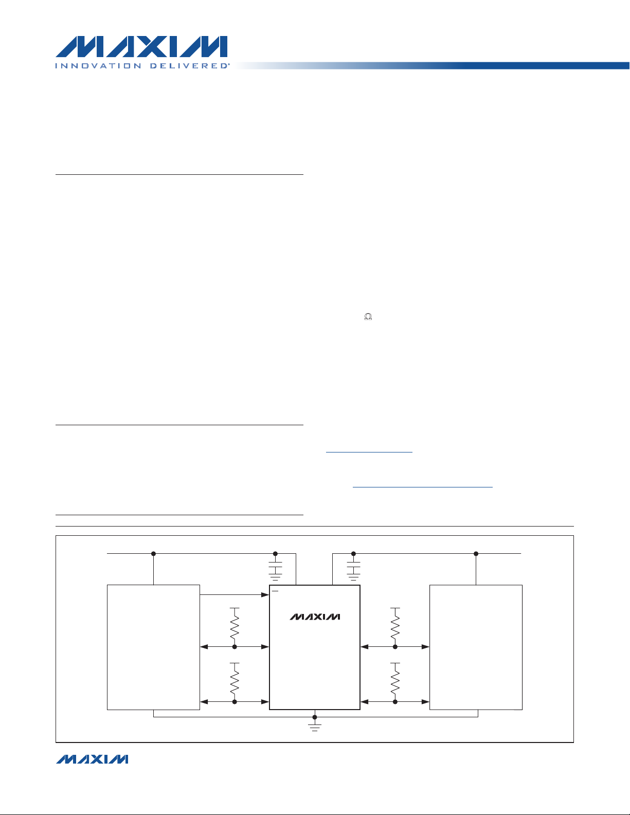
Typical Operating Circuit
+3V
SYSTEM
GND
V
CC
= +3.0V
VL = +1.2V
IOVCC1
IOVCC2
1µF
V
CC
*
V
CC
*
SLK
0.1µF
MAX14595
GND
V
CC
V
+1.2V
SYSTEM
CONTROLLER
GND
* PULLUPS ARE OPTIONAL FOR HIGH-SPEED, OPEN-DRAIN OPERATION.
����������������������������������������������������������������� Maxim Integrated Products 1
EN TS
SDA
SLK
V
L
*
V
L
*
L
IOVL1 SDA
IOVL2
For pricing, delivery, and ordering information, please contact Maxim Direct at 1-888-629-4642,
or visit Maxim’s website at www.maxim-ic.com.

MAX14595
Low-Power Dual-Channel Logic-Level Translator
ABSOLUTE MAXIMUM RATINGS
Voltages referenced to GND.
VCC, VL, TS .............................................................-0.5V to +6V
IOVCC1, IOVCC2 ................................... -0.5V to +(VCC + 0.5V)
IOVL1, IOVL2 ............................................-0.5V to +(VL + 0.5V)
Short-Circuit Duration IOVCC1, IOVCC2,
IOVL1, IOVL2 to GND ...........................................Continuous
VCC, IOVCC_ Maximum Continuous Current at +110NC ....100mA
VL IOVL_ Maximum Continuous Current at +110NC ..........40mA
Stresses beyond those listed under “Absolute Maximum Ratings” may cause permanent damage to the device. These are stress ratings only, and functional operation of the device at these or any other conditions beyond those indicated in the operational sections of the specifications is not implied. Exposure to absolute
maximum rating conditions for extended periods may affect device reliability.
PACKAGE THERMAL CHARACTERISTICS (Note 1)
TDFN
Junction-to-Ambient Thermal Resistance (BJA) ........162NC/W
Junction-to-Case Thermal Resistance (BJC) ...............20NC/W
Note 1: Package thermal resistances were obtained using the method described in JEDEC specification JESD51-7, using a four-
layer board. For detailed information on package thermal considerations, refer to www.maxim-ic.com/thermal-tutorial.
TS Maximum Continuous Current at +110NC .....................70mA
Continuous Power Dissipation (TA = +70NC)
TDFN (derate 6.2mW/NC above +70NC) ......................496mW
WLP (derate 11.8mW/NC above +70NC)......................944mW
Operating Temperature Range .......................... -40NC to +85NC
Storage Temperature Range ............................ -65NC to +150NC
Lead Temperature (TDFN only, soldering, 10s) .............+300NC
Soldering Temperature (reflow) ......................................+260NC
WLP
Junction-to-Ambient Thermal Resistance (BJA) ..........85NC/W
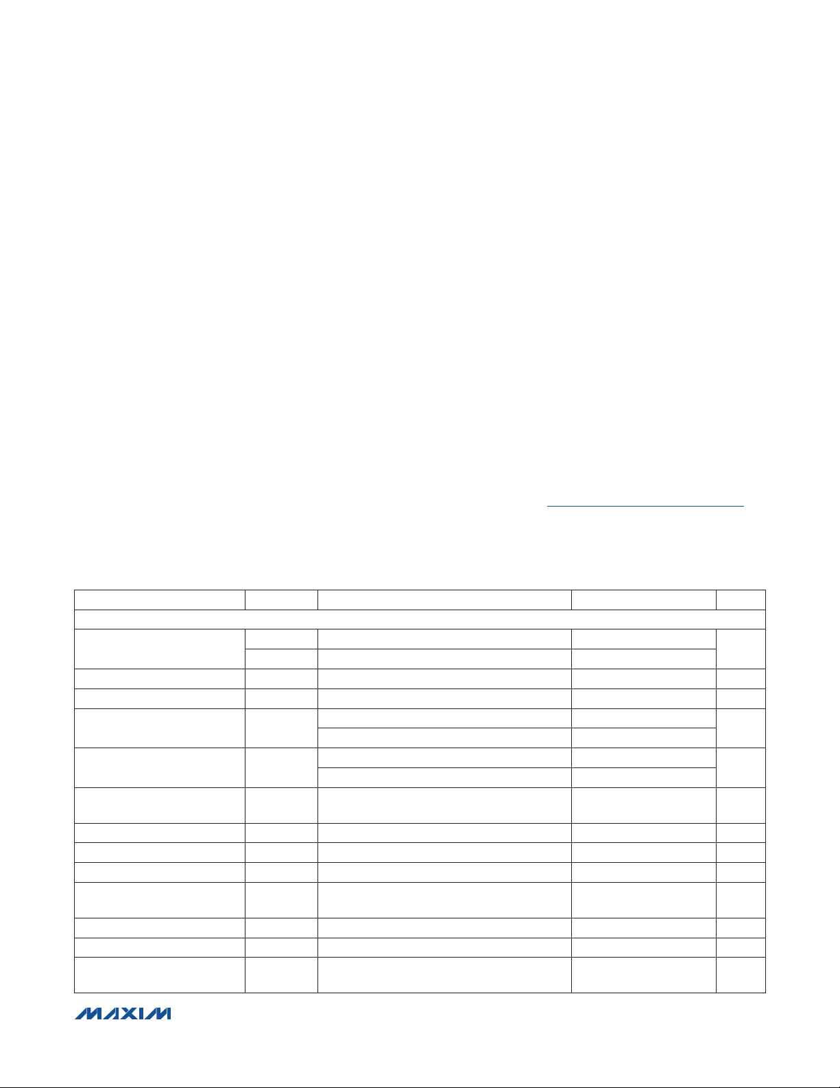
ELECTRICAL CHARACTERISTICS
(V
= +1.65V to +5.5V, V
CC
VCC = +3V, V
POWER SUPPLY
Power Supply Range
VCC Supply Current I
VL Supply Current I
VCC Shutdown Supply Current I
VL Shutdown Supply Current I
IOVCC_, IOVL_ Three-State
Leakage Current
TS Input Leakage Current
VCC Shutdown Threshold V
VL Shutdown Threshold V
VL Above VCC Shutdown
Threshold
IOVL_ Pullup Resistor R
IOVCC_ Pullup Resistor R
IOVL_ to IOVCC_ DC
Resistance
= +1.2V, and TA = +25NC.) (Notes 2, 3)
L
PARAMETER SYMBOL CONDITIONS MIN TYP MAX UNITS
= +0.9V to min(VCC + 0.3V, +3.6V), TA = -40NC to +85NC, unless otherwise noted. Typical values are at
L
V
L
V
CC
CC
L
CC-SHDN
L-SHDN
I
LEAK
I
LEAK_TS
TH_VCC
TH_VL
V
TH_VL-VCCVL
VL_PU
VCC_PU
R
IOVL-IOVCC
IOVCC_ = VCC, IOVL_ = VL, TS = V
IOVCC_ = VCC, IOVL_ = VL, TS = V
TS = GND
TS = VCC, VL = GND, IOVCC_ = unconnected
TS = GND
TS = VL, VCC = GND, IOVL_ = unconnected
TA = +25NC, TS = GND
TA = +25NC
TS = VL, VCC falling
TS = VCC, VL falling, V
Inferred from V
Inferred from V
Inferred from V
0.9 5.5
1.65 5.5
CC
CC
L = 0.9V
rising above VCC, VCC = +1.65V 0.4 0.73 1.1 V
measurements 3 7.6 12
OHL
measurements 3 7.6 12
OHC
measurements 6 17
OLx
0.25 0.6 0.86 V
7 15
3 6
0.4 1
0.4 1
0.1 1
0.1 1
0.1 1
1
0.8 1.35 V
V
FA
FA
FA
FA
FA
FA
kI
kI
I
����������������������������������������������������������������� Maxim Integrated Products 2

MAX14595
Low-Power Dual-Channel Logic-Level Translator
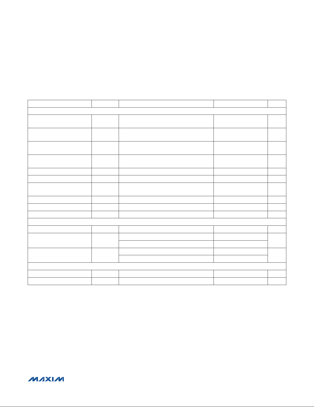
ELECTRICAL CHARACTERISTICS (continued)
(V
= +1.65V to +5.5V, V
CC
VCC = +3V, V
= +1.2V, and TA = +25NC.) (Notes 2, 3)
L
PARAMETER SYMBOL CONDITIONS MIN TYP MAX UNITS
LOGIC LEVELS
IOVL_ Input-Voltage High V
IOVL_ Input-Voltage Low V
IOVCC_ Input-Voltage High V
IOVCC_ Input-Voltage Low V
TS Input-Voltage High
TS Input-Voltage Low
IOVL_ Output-Voltage High V
IOVL_ Output-Voltage Low V
IOVCC_ Output-Voltage High V
IOVCC_ Output-Voltage Low V
RISE/FALL TIME ACCELERATOR STAGE
Accelerator Pulse Duration VL = +0.9V, VCC = +1.65V 9 22 48 ns
IOVL_ Output Accelerator
Source Impedance
IOVCC_ Output Accelerator
Source Impedance
THERMAL PROTECTION
Thermal Shutdown T
Thermal Hysteresis T
= +0.9V to min(VCC + 0.3V, +3.6V), TA = -40NC to +85NC, unless otherwise noted. Typical values are at
L
IHL
ILL
IHC
ILC
V
IH
V
IL
OHL
OLL
OHC
OLC
IOVL_ rising, VL = +0.9V, VCC = +1.65V
(Note 4)
IOVL_ falling, VL = +0.9V, VCC = +1.65V
(Note 4)
IOVCC_ rising, VL = +0.9V, VCC = +1.65V
(Note 4)
IOVCC_ falling, VL = +0.9V, VCC = +1.65V
(Note 4)
TS rising, VL = +0.9V or +3.6V, VCC > V
TS falling, VL = +0.9V or +3.6V, VCC > V
IOVL_ source current 20FA, V
IOVCC_
L
L
= VL to
VCC (VCC R VL)
IOVL_ sink current 5mA, V
IOVCC_ source current 20FA, V
IOVCC_ sink current 5mA, V
IOVCC_
IOVL_
P 0.05V
IOVL_
P 0.05V
= VL
VL - 0.2 V
0.15 V
VCC - 0.4 V
0.2 V
VL - 0.15 V
0.2 V
0.7 x V
L
0.2 V
0.7 x V
CC
0.25 V
VL = +0.9V, IOVL_ = GND, VCC = +1.65V 26
VL = +3.3V, IOVL_ = GND, VCC = +5V 6.8
VCC = +1.65V, IOVCC_ = GND 26
VCC = +5V, IOVCC_ = GND 6.5
SHDN
HYST
+150
10
V
V
I
I
NC
NC
����������������������������������������������������������������� Maxim Integrated Products 3

MAX14595
Low-Power Dual-Channel Logic-Level Translator
TIMING CHARACTERISTICS
(V
= +1.65V to +5.5V, V
CC
TA = -40NC to +85NC, unless otherwise noted. Typical values are at VCC = +3V, V
for rise time and 90% to 10% for fall time.) (Note 5)
PARAMETER SYMBOL CONDITIONS MIN TYP MAX UNITS
Turn-On Time for Q1 t
IOVCC_ Rise Time t
IOVCC_ Fall Time t
IOVL_ Rise Time t
IOVL_ Fall Time t
Propagation Delay
(Driving IOVL_)
Propagation Delay
(Driving IOVCC_)
Channel-to-Channel Skew t
Maximum Data Rate
Note 2: All devices are 100% production tested at TA = +25NC. Limits over the operating temperature range are guaranteed by
design and not production tested.
Note 3: VL must be less than or equal to VCC during normal operation. However, VL can be greater than VCC during startup and
shutdown conditions.
Note 4: V
Note 5: Guaranteed by design.
Note 6: External pullup resistors are required.
IHL
, V
ILL
, V
= +0.9V to +3.6V, VCC R VL, TS = VL, C
L
V
TS
Push-pull driving, VL = +1.2V, VCC = +3V
(Figure 1)
Open-drain driving, VL = +1.2V, VCC = +3V
(Figure 2)
Push-pull driving, VL = +1.2V, VCC = +3V
(Figure 1)
Open-drain driving, VL = +1.2V, VCC = +3V
(Figure 2)
Push-pull driving, VL = +1.2V, VCC = +3V
(Figure 3)
Open-drain driving, VL = +1.2V, VCC = +3V
(Figure 4)
Push-pull driving, VL = +1.2V, VCC = +3V
(Figure 3)
Open-drain driving, VL = +1.2V, VCC = +3V
(Figure 4)
Push-pull driving,
VL = +1.2V, VCC = +3V
(Figure 1)
Push-pull driving,
VL = +1.2V, VCC = +3V
(Figure 3)
Input rise time/fall time < 6ns 1.5 ns
Push-pull operation 8
Open-drain operation (Note 6) 4
IHC
, and V
ON
RCC
FCC
RL
FL
t
PD_LCC
t
PD_CCL
SKEW
are intended to define the range where the accelerator triggers.
ILC
= 1FF, CVL = 0.1FF, C
VCC
= 0V to VL (see the Block Diagram)
= +1.2V and TA = +25NC. All timing is 10% to 90%
L
Rising 7.6 19
Falling 3 9
Rising 3 5
Falling 1.5 7
IOVL_
P 100pF, C
160 400
8 22
11
5 15
6
4 13
16
2.8 12
3.3
IOVCC_
P 100pF,
Fs
ns
ns
ns
ns
ns
ns
MHz
����������������������������������������������������������������� Maxim Integrated Products 4

MAX14595
Low-Power Dual-Channel Logic-Level Translator
V
L
V
L
TS
R
50I
S
MAX14595
IOVL_
GND
t
RCC
90%
50%
50%
t
PD_LCC
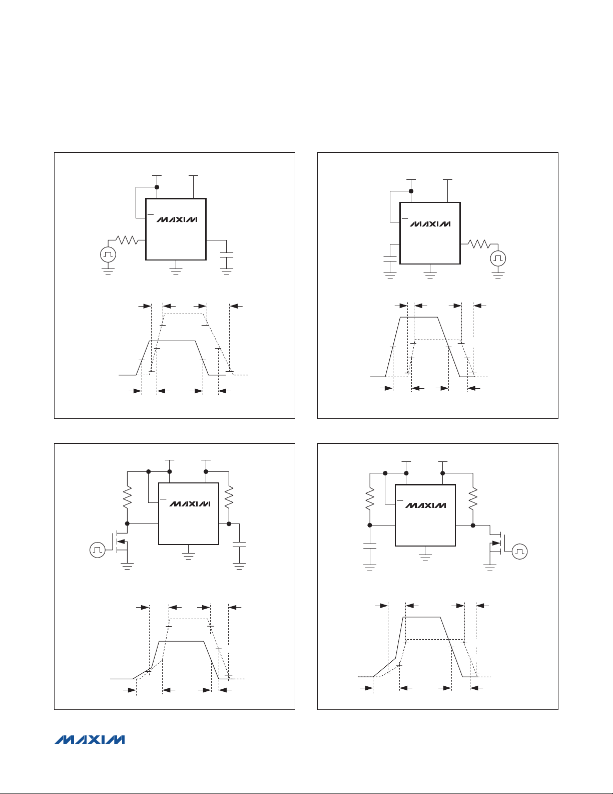
Figure 1. Push-Pull Driving IOVL_
V
L
V
CC
V
CC
IOVCC_
90%
50%
50%
t
PD_LCC
V
V
L
V
L
TS
C
L
20pF
t
FCC
20pF
IOVL_
C
L
t
RL
50%
10%10%
t
PD_CCL
MAX14595
GND
90%
50%
50%
V
CC
V
CC
IOVCC_
t
PD_CCL
R
S
50I
t
FL
90%
50%
10%10%
Figure 3. Push-Pull Driving IOVCC_
CC
V
L
V
CC
V
1kI 1kI
L
TS
MAX14595
IOVL_
R
5I
DSON
GND
t
RCC
90%90%
10%
t
PD_LCC
Figure 2. Open-Drain Driving IOVL_
����������������������������������������������������������������� Maxim Integrated Products 5
V
CC
IOVCC_
50%
t
t
FCC
PD_LCC
50%
10%
C
L
20pF
V
1kI 1kI
L
TS
V
CC
MAX14595
20pF
IOVL_
C
L
t
RL
90%
IOVCC_
GND
50%
10%
t
PD_CCL
t
PD_CCL
Figure 4. Open-Drain Driving IOVCC_
t
FL
90%
R
DSON
50%
5I
10%

MAX14595
Low-Power Dual-Channel Logic-Level Translator
Typical Operating Characteristics
(VCC = +3V, VL = +1.5V, RL = 1MI, CL = 15pF, push-pull driving data rate = 8Mbps, TA = +25NC, unless otherwise noted.)
VL DYNAMIC SUPPLY CURRENT vs. VCC SUPPLY
VOLTAGE (OPEN-DRAIN DRIVING ONE IOVL_)
200
180
160
140
120
100
80
SUPPLY CURRENT (µA)
60
L
V
40
20
0
1.65 5.50
VCC (V)
4.954.403.30 3.852.752.20
VCC DYNAMIC SUPPLY CURRENT vs. VL SUPPLY
VOLTAGE (OPEN-DRAIN DRIVING ONE IOVCC_)
800
700
600
500
400
300
SUPPLY CURRENT (µA)
CC
V
200
100
0
0.9 3.6
VL (V)
3.33.01.2 1.5 1.8 2.42.1 2.7
VL DYNAMIC SUPPLY CURRENT vs. CAPACITIVE
LOAD (OPEN-DRAIN DRIVING ONE IOVL_)
200
180
160
140
120
100
80
SUPPLY CURRENT (µA)
60
L
V
40
20
0
0 100
CAPACITIVE LOAD (pF)
80604020
VL DYNAMIC SUPPLY CURRENT vs. VCC SUPPLY
VOLTAGE (PUSH-PULL DRIVING ONE IOVCC_)
200
180
MAX14595 toc01
160
140
120
100
80
SUPPLY CURRENT (µA)
60
L
V
40
20
0
1.65 5.50
VCC (V)
VL DYNAMIC SUPPLY CURRENT vs. TEMPERATURE
(OPEN-DRAIN DRIVING ONE IOVL_)
200
180
MAX14595 toc04
160
140
120
100
80
SUPPLY CURRENT (µA)
60
L
V
40
20
0
-40 85
TEMPERATURE (°C)
VCC DYNAMIC SUPPLY CURRENT vs. CAPACITIVE
LOAD (PUSH-PULL DRIVING ONE IOVL_)
1.6
1.4
MAX14595 toc07
1.2
1.0
0.8
0.6
SUPPLY CURRENT (mA)
CC
0.4
V
0.2
0
0 100
CAPACITIVE LOAD (pF)
VCC DYNAMIC SUPPLY CURRENT vs. VL SUPPLY
VOLTAGE (PUSH-PULL DRIVING ONE IOVL_)
800
700
MAX14595 toc02
600
500
400
300
SUPPLY CURRENT (µA)
CC
V
200
100
4.954.403.30 3.852.752.20
0
0.9 3.6
VL (V)
VL DYNAMIC SUPPLY CURRENT vs. TEMPERATURE
(PUSH-PULL DRIVING ONE IOVCC_)
200
180
MAX14595 toc05
160
140
120
100
80
SUPPLY CURRENT (µA)
60
L
V
40
20
603510-15
0
-40 85
TEMPERATURE (°C)
RISE/FALL TIME vs. CAPACITIVE LOAD
(PUSH-PULL DRIVING ONE IOVL_)
35
RS = 50Ω
MAX14595 toc08
806020 40
30
25
20
15
RISE/FALL TIME (ns)
10
5
0
0 100
t
FCC
CAPACITIVE LOAD (pF)
t
RCC
MAX14595 toc03
3.33.01.2 1.5 1.8 2.42.1 2.7
MAX14595 toc06
603510-15
MAX14595 toc09
80604020
����������������������������������������������������������������� Maxim Integrated Products 6

MAX14595
06
Low-Power Dual-Channel Logic-Level Translator
Typical Operating Characteristics (continued)
(VCC = +3V, VL = +1.5V, RL = 1MI, CL = 15pF, push-pull driving data rate = 8Mbps, TA = +25NC, unless otherwise noted.)
PROPAGATION DELAY vs. CAPACITIVE LOAD
(PUSH-PULL DRIVING ONE IOVL_)
16
RS = 50Ω
14
12
10
PROPAGATION DELAY (ns)
t
PD_LCC_RISE
8
6
4
2
0
0 100
t
PD_LCC_FALL
CAPACITIVE LOAD (pF)
9
8
7
6
(Ω)
5
4
IOVL-IOVCC
R
3
2
1
0
806020 40
R
IOVL-IOVCC
VCC = 1.65V
VCC = 3.3V
VL (V)
vs. V
V
I
MAX14595 toc10
L
VCC = 5.5V
IOVL_
IOVCC_
RISE/FALL TIME vs. CAPACITIVE LOAD
(PUSH-PULL DRIVING ONE IOVCC_)
16
RS = 50Ω
14
12
10
8
6
RISE/FALL TIME (ns)
4
2
0
0 100
t
FL
t
RL
CAPACITIVE LOAD (pF)
RAIL-TO-RAIL DRIVING (PUSH-PULL DRIVING ONE IOVL_)
= +1.5V, VCC = +3.3V, CL = 15pF, RL = 1MΩ, RS = 50Ω)
(V
L
MAX14595 toc13
= 0.05V
= 3.3mA
54321
PROPAGATION DELAY vs. CAPACITIVE LOAD
(PUSH-PULL DRIVING ONE IOVCC_)
8
RS = 50Ω
MAX14595 toc11
806020 40
7
6
5
4
3
PROPAGATION DELAY (ns)
2
1
0
0 100
40ns/div
t
PD_CCL_FALL
t
PD_CCL_RISE
CAPACITIVE LOAD (pF)
MAX14595 toc14
IOVL_
1V/div
IOVCC_
1V/div
MAX14595 toc12
806020 40
RAIL-TO-RAIL DRIVING (OPEN-DRAIN DRIVING ONE IOVL_)
= +1.5V, VCC = +3.3V, CL = 100pF, RL = 50Ω,
(V
L
R
= 50Ω, PULLUP ON IOVL_/IOVCC_ = 1kΩ)
S
40ns/div
MAX14595 toc15
IOVL_
1V/div
IOVCC_
1V/div
����������������������������������������������������������������� Maxim Integrated Products 7
EXITING SHUTDOWN MODE
= 1.2V, VCC = 3.0V, IOVCC_ = 0V,
(V
L
C
= 100pF, R
L
40µs/div
PU_VL
= 50Ω)
MAX14595 toc16
TS
500mV/div
IOVL_
500mV/div

MAX14595
Low-Power Dual-Channel Logic-Level Translator
Pin Configurations
TOP VIEW
BUMPS ON BOTTOM
12
+
A
V
IOVL2
L
B
IOVCC2
V
CC
MAX14595
IOVL1
IOVCC1
WLP
V
CC
865
3
4
TS
GND
134
+
V
L
IOVCC2
7
MAX14595
2
IOVL2
TDFN
IOVCC1
IOVL1
GND
TS
BUMP/PIN
WLP TDFN
A1 1 V
NAME FUNCTION
Logic Supply Voltage, +0.9V to min(VCC + 0.3V, +3.6V). Bypass VL to GND with a 0.1FF
L
ceramic capacitor as close as possible to the device.
A2 2 IOVL2 Input/Output 2. Reference to VL.
A3 3 IOVL1 Input/Output 1. Reference to VL.
Active Low Three-State Input. Drive TS low to place the device in shutdown mode with
A4 4
TS
high-impedance output and internal pullup resistors disconnected. Drive TS high for normal
operation.
B1 8 V
Power-Supply Voltage, +1.65V to +5.5V. Bypass VCC to GND with a 1FF ceramic capacitor
CC
as close as possible to the device.
B2 7 IOVCC2 Input/Output 2. Reference to VCC.
B3 6 IOVCC1 Input/Output 1. Reference to VCC.
B4 5 GND Ground
Pin Description
����������������������������������������������������������������� Maxim Integrated Products 8

MAX14595
Low-Power Dual-Channel Logic-Level Translator
Block Diagram
V
L
MAX14595
ONE-SHOOT
BLOCK
EN CONTROL
BLOCK
GATE
DRIVE
IOVL_
NQ1
Detailed Description
The MAX14595 is a dual-channel, bidirectional level translator. The device translates low voltage down to +0.9V on
the VL side to high voltage on the VCC side and vice-versa. The device is optimized for open-drain and high-speed
operation, such as I2C bus and MDIO bus.
The device has low on-resistance (17I max), which
is important for high-speed, open-drain operation. The
device also features internal pullup resistors that are
active when the corresponding power is on and TS is high.
Level Translation
For proper operation, ensure that +1.65V P VCC P +5.5V,
and +0.9V P VL P VCC. When power is supplied to VL
while VCC is less than VL, the device automatically
disables logic-level translation function. Also, the device
enters shutdown mode when TS = GND.
High-Speed Operation
The device meets the requirements of high-speed I2C
and MDIO open-drain operation. The maximum data rate
is at least 4MHz for open-drain operation with the total
bus capacitance equal to or less than 100pF.
V
CCTS
ONE-SHOOT
BLOCK
IOVCC_
Three-State Input TS
The device features a three-state input that can put the
device into high-impedance mode. When TS is low,
IOVCC_ and IOVL_ are all high impedance and the internal pullup resistors are disconnected. When TS is high,
the internal pullup resistors are connected when the
corresponding power is in regulation, and the resistors
are disconnected at the side that has no power on. In
many portable applications, one supply is turned off but
the other side is still operating and requires the pullup
resistors to be present. This feature eliminates the need
for external pullup resistors. The level translation function
is off until both power supplies are in range.
Thermal-Shutdown Protection
The device features thermal-shutdown protection to
protect the part from overheating. The device enters
thermal shutdown when the junction temperature exceeds
+150NC (typ), and the device is back to normal operation
again after the temperature drops by approximately 10NC
(typ). When the device is in thermal shutdown, the level
translator is disabled.
����������������������������������������������������������������� Maxim Integrated Products 9

MAX14595
Low-Power Dual-Channel Logic-Level Translator
Ordering Information
PART TOP MARK PIN-PACKAGE
MAX14595ETA+T BNS 8 TDFN
MAX14595EWA+T AAD 8 WLP
Note: All devices are specified over -40°C to +85°C operating
temperature range.
+Denotes a lead(Pb)-free/RoHS-compliant package.
T = Tape and reel.
Chip Information
PROCESS: BiCMOS
Package Information
For the latest package outline information and land patterns
(footprints), go to www.maxim-ic.com/packages. Note that a
“+”, “#”, or “-” in the package code indicates RoHS status only.
Package drawings may show a different suffix character, but
the drawing pertains to the package regardless of RoHS status.
PACKAGE
TYPE
8 TDFN T822CN+1
8 WLP W80A1+1
PACKAGE
CODE
OUTLINE
NO.
21-0487 90-0349
21-0555
LAND
PATTERN NO.
Refer to
Application
Note 1891
���������������������������������������������������������������� Maxim Integrated Products 10

MAX14595
Low-Power Dual-Channel Logic-Level Translator
Revision History
REVISION
NUMBER
0 12/11 Initial release —
REVISION
DATE
DESCRIPTION
PAGES
CHANGED
Maxim cannot assume responsibility for use of any circuitry other than circuitry entirely embodied in a Maxim product. No circuit patent licenses are implied.
Maxim reserves the right to change the circuitry and specifications without notice at any time. The parametric values (min and max limits) shown in the Electrical
Characteristics table are guaranteed. Other parametric values quoted in this data sheet are provided for guidance.
Maxim Integrated Products, 120 San Gabriel Drive, Sunnyvale, CA 94086 408-737-7600 11
©
2011 Maxim Integrated Products Maxim is a registered trademark of Maxim Integrated Products, Inc.
 Loading...