

General Description
The MAX14504/MAX14505/MAX14505A/MAX14506
dual single-pole/double-throw (SPDT) audio switches
feature negative signal capability that allows signals
from -VCCto +VCCto pass without distortion. They feature high continuous current ratings of 550mA (continuous) and 850mA (pulsed). These analog switches have
low on-resistance, low supply current, and operate from
a single +2.3V to +5.5V supply.
The MAX14505/MAX14505A have internal shunt switches
that discharge the audio amplifier AC-coupling capacitance at the normally open (NO) terminals. This reduces
click-and-pop sounds that occur when switching audio
signals between precharged points. The MAX14504/
MAX14505/MAX14505A/MAX14506 control the switches
with control bit, CB, and feature an enable input, EN, that
place COM in a high-impedance mode.
The MAX14504/MAX14505/MAX14505A/MAX14506 are
fully specified to operate from a single +2.3V to +5.5V
power supply. These devices are available in a 1.56mm
x 2.14mm, 12-bump WLP package, and operate over
the -40°C to +85°C extended temperature range.
Applications
Cell Phones
MP3 Players
Portable Audio Equipment
Speaker Switching
Features
o Distortion-Free Negative Signal Throughput from
-VCCto +V
CC
o Internal Shunt Switches Reduce Click/Pop
(MAX14505/MAX14505A)
o Low On-Resistance 0.36Ω (typ)
o 1mΩ (typ) On-Resistance Flatness
o COM High Impedance for EN = High
o Low 0.2µA (max) Shutdown Current
(MAX14505A/MAX14506)
o +2.3V to +5.5V Single-Supply Voltage
o Small, 1.56mm x 2.14mm, 12-Bump WLP Package
MAX14504/MAX14505/MAX14505A/MAX14506
Dual SPDT Negative Rail Analog Switches
with ±V
CC
Capability
________________________________________________________________
Maxim Integrated Products
1
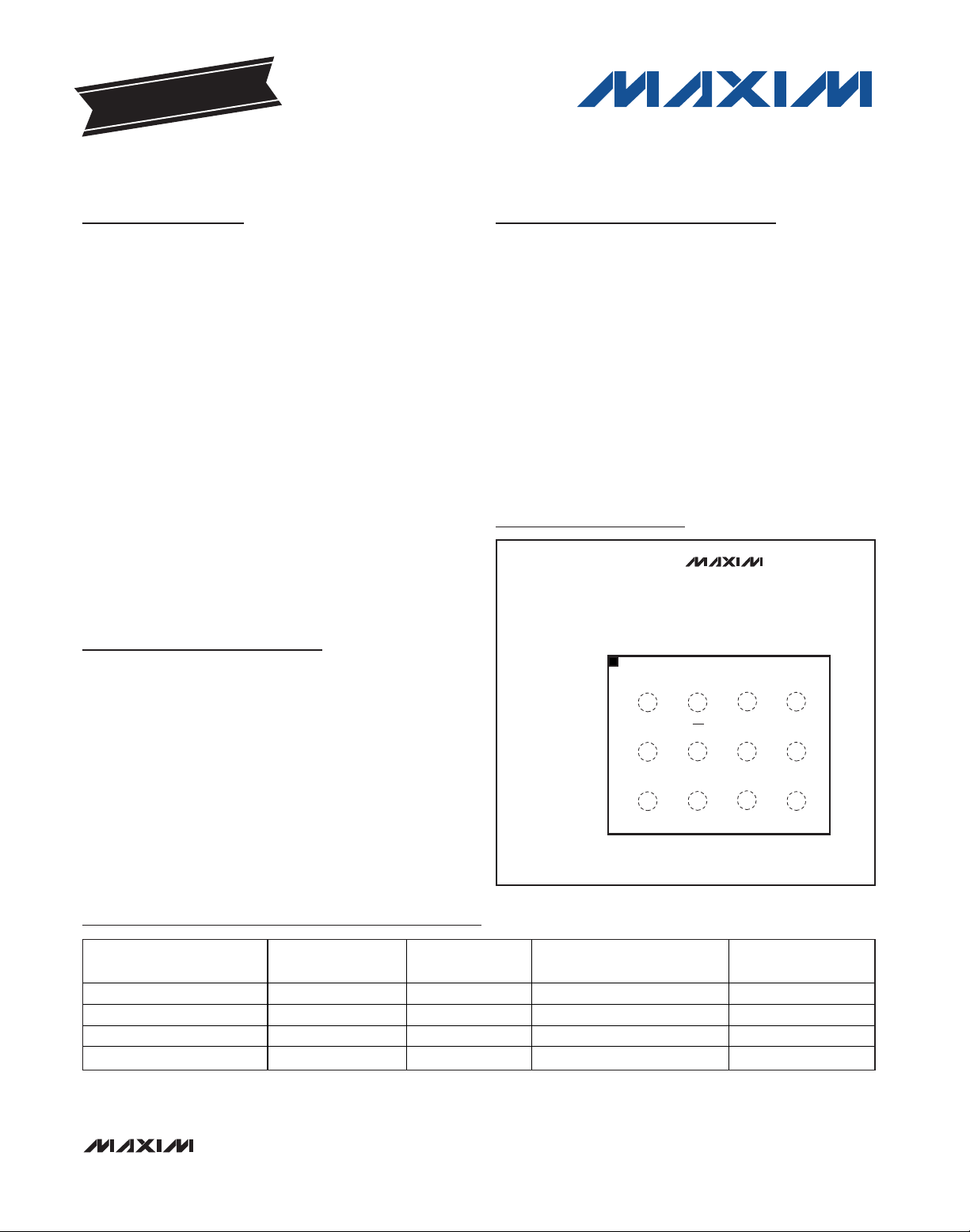
Pin Configuration
Ordering Information/Selector Guide
19-4244; Rev 1; 12/08
For pricing, delivery, and ordering information, please contact Maxim Direct at 1-888-629-4642,
or visit Maxim’s website at www.maxim-ic.com.
EVALUATION KIT
AVAILABLE
PART PIN-PACKAGE TOP MARK
COM SIGNAL RANGE FOR
EN = V
CC
CLICKLESS
MAX14504EWC+ 12 WLP AAH ±V
CC
NO
MAX14505EWC+* 12 WLP AAI ±V
CC
YES
MAX14505AEWC+ 12 WLP AAK 0 to +V
CC
YES
MAX14506EWC+* 12 WLP AAJ 0 to +V
CC
NO
Note: All devices are specified over the -40°C to +85°C temperature range.
+
Denotes a lead(Pb)-free/RoHS-compliant package.
*
Future product—contact factory for availability.
Typical Operating Circuit appears at end of data sheet.
MAX14504/
TOP VIEW
(BUMPS ON BOTTOM)
1
+
NO2
A
COM2 GND COM1
B
MAX14505/
MAX14505A/
MAX14506
234
NEG
V
EN
NO1
CC
NC2 NC1
C
(1.56mm x 2.14mm)
CB
WLP
GND
MAX14504/MAX14505/MAX14505A/MAX14506
Dual SPDT Negative Rail Analog Switches
with ±V
CC
Capability
2 _______________________________________________________________________________________
ABSOLUTE MAXIMUM RATINGS
ELECTRICAL CHARACTERISTICS
(VCC= +2.3 to +5.5V, TA= T
MIN
to T
MAX,CNEG
= 3.3nF, unless otherwise noted. Typical values are at VCC= +3.0V, TA= +25°C,
unless otherwise noted.) (Note 3)
Stresses beyond those listed under “Absolute Maximum Ratings” may cause permanent damage to the device. These are stress ratings only, and functional
operation of the device at these or any other conditions beyond those indicated in the operational sections of the specifications is not implied. Exposure to
absolute maximum rating conditions for extended periods may affect device reliability.
Note 1: Signals on NC_, NO_, and COM_ exceeding -VCCor +VCCare clamped by internal diodes. For EN ≥ VIHsignals on NC_,
NO_, and COM_ exceeding 0 or +V
CC
are clamped by internal diodes (MAX14505A/MAX14506). Limit forward-diode current
to maximum current rating.
Note 2: Package thermal resistances were obtained using the method described in JEDEC specification JESD51-7, using a 4-layer
board. For detailed information on package thermal considerations, refer to www.maxim-ic.com/thermal-tutorial
.
(All voltages referenced to GND, unless otherwise noted.)
V
CC
........................................................................-0.3V to +6.0V
NC_, NO_, COM_ (Note 1)..................-V
CC
- 0.3V to VCC+ 0.3V
NC_, NO_, COM_ (MAX14505A/MAX14506, EN = V
CC
)
(Note 1).......................................................-0.3V to V
CC
+ 0.3V
CB, EN......................................................................-0.3V to +6V
Continuous Current (NC_, NO_, COM_).........................±550mA
Continuous Current on Shunt Switches ..............................±5mA
Peak Current (NC_, NO_, COM_)
(pulsed at 1ms, 10% duty cycle)..................................±850mA
Continuous Power Dissipation (T
A
= +70°C) for multilayer board:
12-Pin WLP (derate 8.5mW/°C above +70°C) ..............678mW
Operating Temperature Range ...........................-40°C to +85°C
Junction Temperature......................................................+150°C
Storage Temperature Range .............................-65°C to +150°C
Package Junction-to-Ambient Thermal
Resistance (θ
JA
) (Note 2)............................................118°C/W
Lead Temperature (soldering) .........................................+300°C
)
PARAMETER SYMBOL CONDITIONS MIN TYP MAX UNITS
ANALOG SWITCH
V EN = 0 -V
Analog Signal Range
On-Resistance R
On-Resistance Match
Between Channels
On-Resistance Flatness R
Shunt Switch Resistance R
NC_, NO_,
COM_
ON
∆R
ON
FLAT (ON
SHUNT
V
= V
EN
CC
VCC = +3.0V,
= 50mA,
I
COM_
V
, V
NC_
-V
CC
VCC = +3.0V, I
between NC_ and NO_ only
VCC = +3.0V, I
V
NC_
V
NO_
=
NO_
to V
CC
NC_
, V
= +100mV
NC_
= -VCC to VCC (Note 4)
NO_
(MAX14504/
MAX14505)
(MAX14505A/
MAX14506)
TA = +25°C 0.36 0.5
= I
= I
NO_
NO_
TA = T
T
MAX
= 50mA;
= 50mA,
MIN
to
CC
-V
CC
0+V
10 mΩ
1mΩ
15 55 120 Ω
+V
+V
0.65
CC
CC
CC
V
Ω
MAX14504/MAX14505/MAX14505A/MAX14506
Dual SPDT Negative Rail Analog Switches
with ±V
CC
Capability
_______________________________________________________________________________________ 3
(
)
)
(
(
(ON)
ELECTRICAL CHARACTERISTICS (continued)
(VCC= +2.3 to +5.5V, TA= T
MIN
to T
MAX,CNEG
= 3.3nF, unless otherwise noted. Typical values are at VCC= +3.0V, TA= +25°C,
unless otherwise noted.) (Note 3)
PARAMETER SYMBOL CONDITIONS MIN TYP MAX UNITS
NC_ or NO_ Off-Leakage
Current
COM_ On-Leakage
Current
DYNAMIC TIMING (Note 5)
Turn-On Time t
Turn-Off Time t
AUDIO PERFORMANCE
Total Harmonic Distortion Plus
Noise
Off-Isolation V
Crosstalk V
NC_ or NO_ Off-Capacitance
COM_ On-Capacitance C
LOGIC INPUT (CB, EN)
Input Logic-High V
Input Logic-Low V
Input Leakage Current I
INC_
I
NO_ (OFF
I
COM_ (ON
THD+N
C
N C
C
N O
COM
ON
OFF
ISO
CT
_
_
_
IH
IL
IN
VCC = +3.0V, switch open;
= -2.5V, +2.5V;
V
NO_
V
= +2.5V, -2.5V, unconnected
COM_
,
OF F)
(MAX14504/MAX14506)
VCC = +3.0V, switch open;
= -2.5V, +2.5V;
V
NC_
V
= +2.5V, -2.5V, unconnected
COM_
V
= + 3.0V , sw i tch cl osed ;
C C
= + 2.5V , - 2.5V ;
V
C OM _
V
or V
N C _
V
NO_
V
NO_
f = 20Hz to 20kHz, V
= RL = 50Ω; DC bias = 0
R
S
RS = RL = 50Ω; V
f = 20kHz (Note 6), Figure 2
RS = RL = 50Ω; V
f = 20kHz (Note 7), Figure 2
,
OF F)
V
OF F)
NC_/NO_
V
NC_/NO_
VCB = V EN = 0 or V
= + 2.5V , - 2.5V , unconnected
N O_
or V
or V
= 0, RL = 50Ω, Figure 1 14 60 ms
NC_
= 0, RL = 50Ω, Figure 1 1.5 3 µs
NC_
COM
COM
= 0.5V
P-P
= 0.5V
P-P
= 0.5V
COM_
_ = 0.5V
_ = 0.5V
, f = 1MHz; Figure 3 65 pF
, f = 1MHz; Figure 3 125 pF
CC
P-P
P-P
P-P
,
,
,
-50 +50
-50 +50
-100 +100 nA
1.4 V
-1 +1 µA
0.001 %
-84 dB
-90 dB
0.5 V
nA
MAX14504/MAX14505/MAX14505A/MAX14506
Dual SPDT Negative Rail Analog Switches
with ±V
CC
Capability
4 _______________________________________________________________________________________
Note 3: All parameters are production tested at TA= +85°C, and guaranteed by design over the specified temperature range.
Note 4: Flatness is defined as the difference between the maximum and minimum value of on-resistance as measured over the
specified analog signal range.
Note 5: All timing is measured using 20% and 80% levels.
Note 6: Off-Isolation = 20log
10[VCOM_
/(V
NO_
or V
NC_
)], V
COM_
= output, V
NO_
or V
NC_
= input to off switch.
Note 7: Between any two switches.
ELECTRICAL CHARACTERISTICS (continued)
(VCC= +2.3 to +5.5V, TA= T
MIN
to T
MAX,CNEG
= 3.3nF, unless otherwise noted. Typical values are at VCC= +3.0V, TA= +25°C,
unless otherwise noted.) (Note 3)
0
0.3
0.2
0.1
0.4
0.5
0.6
0.7
0.8
0.9
1.0
-2.30 -1.15 0 1.15 2.30
ON-RESISTANCE vs. V
COM
MAX14504 toc01
V
COM
(V)
R
ON
(Ω)
VCC = 2.3V
TA = +85°C TA = +25°C TA = -40°C
0
0.3
0.2
0.1
0.4
0.5
0.6
0.7
0.8
0.9
1.0
-3 -1-2 0123
ON-RESISTANCE vs. V
COM
MAX14504 toc02
V
COM
(V)
R
ON
(Ω)
VCC = 3.0V
TA = +85°C TA = +25°C TA = -40°C
0
0.2
0.1
0.5
0.4
0.3
0.6
0.7
0.9
0.8
1.0
-5.5 -3.5-2.5-4.5 -1.5 -0.5 0.5 1.5 2.5 3.5 4.5 5.5
ON-RESISTANCE vs. V
COM
V
COM
(V)
R
ON
(Ω)
VCC = 5.5V
MAX14504 toc03
TA = +85°C TA = +25°C TA = -40°C
Typical Operating Characteristics
(VCC= 3.0V, TA = +25°C, unless otherwise noted.)
PARAMETER SYMBOL CONDITIONS MIN TYP MAX UNITS
POWER SUPPLY
Power-Supply Range V
Power-Supply Rejection Ratio
(PSRR)
VCC Supply Current I
VCC Shutdown Supply Current I
Supply Current Increase with
Supply Voltage
Negative Charge-Pump Output V
CC
R
CC
VCC = +3.0V, V EN = 0, VCB = 0 or V
VCC = +5.5V, V EN = 0, VCB = 0 or V
VCC = +3.0V, V EN = V
(MAX14504/MAX14505)
VCC = +5.5V, V EN = V
(MAX14504/MAX14505)
CC_SHDN
VCC = +3.0V, V EN = V
(MAX14505A/MAX14506)
VCC = +5.5V, V EN = V
(MAX14505A/MAX14506)
I
CC_CTRLVCC
NEG
C
= 50Ω, f = 10kHz 78 dB
COM_
= 5.5V, VCB = V EN = 0.5V or 1.4V 2 5 µA
= 3.3nF - 1.01V
NEG
CC
CC
CC
CC
CC
CC
2.3 5.5 V
12 23
21 41
µA
15
29
µA
0.15
0.2
C C -VCC
- 0.95V
C C
V

MAX14504/MAX14505/MAX14505A/MAX14506
Dual SPDT Negative Rail Analog Switches
with ±V
CC
Capability
_______________________________________________________________________________________ 5
Typical Operating Characteristics (continued)
(VCC= 3.0V, TA = +25°C, unless otherwise noted.)
0.3650
0.3645
0.3640
0.3635
0.3630
-3 0-2 -1 1 2 3
RON FLATNESS vs. V
COM
MAX14504 toc04
V
COM
(V)
R
ON
(Ω)
20
15
10
5
0
2.3 3.93.1 4.7 5.5
NC_/NO_ TURN-ON/TURN-OFF TIME
vs. SUPPLY VOLTAGE
SUPPLY VOLTAGE (V)
t
ON
(ms)
2.0
1.5
1.0
0.5
0
t
OFF
(µs)
MAX14504 toc05
t
ON
t
OFF
20
15
10
5
0
-40 -15 10 35 60 85
NC_/NO_ TURN-ON/TURN-OFF TIME
vs. TEMPERATURE
TEMPERATURE (°C)
t
ON
(ms)
2.0
1.5
1.0
0.5
0
t
OFF
(µs)
MAX14504 toc06
t
ON
t
OFF
0
5
15
10
20
25
SUPPLY CURRENT
vs. SUPPLY VOLTAGE
MAX14504 toc07
SUPPLY VOLTAGE (V)
SUPPLY CURRENT (µA)
2.3 3.93.1 4.7 5.5
CB = EN = 0
10
14
12
18
16
20
22
-40 85
SUPPLY CURRENT
vs. TEMPERATURE
MAX14504 toc08
TEMPERATURE (°C)
SUPPLY CURRENT (µA)
10-15 35 60
CB = EN = 0
VCC = 5.5V
VCC = 3.0V
0
0.6
0.4
0.2
0.8
1.0
1.2
1.4
1.6
1.8
2.0
2.7 3.0 3.3 3.6
LOGIC-INPUT LOW THRESHOLD
vs. SUPPLY VOLTAGE
MAX14504 toc09
SUPPLY VOLTAGE (V)
LOGIC-INPUT LOW THRESHOLD (V)
V
IH
V
IL
0
20
60
40
80
100
SUPPLY CURRENT
vs. CB LOGIC LEVEL
MAX14504 toc10
CB LOGIC LEVEL (V)
SUPPLY CURRENT (µA)
02.21.1 3.3
VCC = 5.5V
EN = 0

MAX14504/MAX14505/MAX14505A/MAX14506
Dual SPDT Negative Rail Analog Switches
with ±V
CC
Capability
6 _______________________________________________________________________________________
Typical Operating Characteristics (continued)
(VCC= 3.0V, TA = +25°C, unless otherwise noted.)
0
10 100
POWER-SUPPLY REJECTION RATIO
vs. FREQUENCY
100
40
20
80
60
MAX14504 toc17
FREQUENCY (kHz)
PSRR (dB)
0
2
1
4
3
5
6
-40 85
COM_ ON-LEAKAGE CURRENT
vs. TEMPERATURE
MAX14504 toc11
TEMPERATURE (°C)
COM_ ON-LEAKAGE CURRENT (nA)
10-15 35 60
V
COM_
= 2.5V
V
NC_/VNO_
= UNCONNECTED
0
100
50
150
250
300
200
-40 85
NC_/NO_ OFF-LEAKAGE CURRENT
vs. TEMPERATURE
MAX14504 toc12
TEMPERATURE (°C)
NC_/NO_ OFF-LEAKAGE CURRENT (pA)
10-15 35 60
V
NC_/VNO_
= 2.5V
V
COM_
= UNCONNECTED
ON-LOSS vs. FREQUENCY
FREQUENCY (MHz)
0.001 1 10 1000.01 0.1 1000
ON-LOSS (dB)
0
-1
-2
-3
-4
-5
-6
MAX14504 toc13
OFF-ISOLATION vs. FREQUENCY
FREQUENCY (MHz)
0.001 1 10 1000.01 0.1 1000
OFF-ISOLATION (dB)
0
-20
-40
-60
-80
-100
MAX14504 toc14
CROSSTALK vs. FREQUENCY
FREQUENCY (MHz)
0.001 1 10 1000.01 0.1 1000
CROSSTALK (dB)
0
-20
-40
-60
-80
-100
MAX14504 toc15
1
0.0001
0.01 0.1 10 100
TOTAL HARMONIC DISTORTION
PLUS NOISE vs. FREQUENCY
0.001
0.01
0.1
MAX14504 toc16
FREQUENCY (kHz)
THD+N (%)
1

MAX14504/MAX14505/MAX14505A/MAX14506
Dual SPDT Negative Rail Analog Switches
with ±V
CC
Capability
_______________________________________________________________________________________ 7
Test Circuits/Timing Diagrams
Figure 1. Switching Time
Figure 2. Off-Isolation and Crosstalk
MAX14504/
MAX14505/
MAX14505A/
MAX14506
VN_= 0V
LOGIC
INPUT
= V
= V
NO_
IN_ (
OR V
R
NC_
V
OUT
RON + R
V
N_
NO_
OR NC_
CB OR
EN
ON
V
CC
V
CC
GND
)
L
NEG
V
= 1.5V
REF
V
R
L
V
OUT
C
NEG
LOGIC
INPUT
SWITCH
OUTPUT
IH
V
IL
0V
V
50%
OUT
t
ON
tR < 5ns
t
< 5ns
F
t
OFF
0.8 x V
0UT
0.2 x V
OUT
V
CC
0.1µF
V
CC
0V OR
V
50Ω
MEASUREMENTS ARE STANDARDIZED AGAINST SHORTS AT IC TERMINALS.
OFF-ISOLATION IS MEASURED BETWEEN COM_ AND OFF. NO_ OR NC_ TERMINAL
ON EACH CROSSTALK IS MEASURED FROM ONE CHANNEL TO THE OTHER CHANNEL.
SIGNAL DIRECTION THROUGH SWITCH IS REVERSED; WORST VALUES ARE RECORDED.
CB
CC
NC1
MAX14504/
MAX14505/
MAX14505A/
MAX14506
GND
COM1
NO1*
NEG
V
C
NEG
V
OUT
NETWORK
ANALYZER
IN
50Ω 50Ω
MEAS REF
50Ω
50Ω
OFF-ISOLATION = 20log
CROSSTALK = 20log
*FOR CROSSTALK, THIS PIN IS NO2.
NC2 AND COM2 ARE OPEN.
V
(
(
OUT
V
V
V
IN
OUT
IN
)
)

MAX14504/MAX14505/MAX14505A/MAX14506
Dual SPDT Negative Rail Analog Switches
with ±V
CC
Capability
8 _______________________________________________________________________________________
Test Circuits/Timing Diagrams (continued)
Pin Description
Figure 3. Channel Off-/On-Capacitance
CAPACITANCE
METER
f = 1MHz
COM_
NC_ OR
NO_
0.1µF
MAX14504/
MAX14505/
MAX14505A/
V
CC
V
CC
MAX14506
GND
NEG
CB
OR V
V
IL
IH
C
NEG
PIN NAME FUNCTION
A1 NO2 Analog Switch 2, Normally Open Terminal
A2 NEG
A3 V
A4 NO1 Analog Switch 1, Normally Open Terminal
B1 COM2 Analog Switch 2, Common Terminal
B2 EN
B3, C3 GND Ground
B4 COM1 Analog Switch 1, Common Terminal
C1 NC2 Analog Switch 2, Normally Closed Terminal
C2 CB Control Bit Input. CB controls switch 1 and switch 2. See the Functional Diagram/Truth Table.
C4 NC1 Analog Switch 1, Normally Closed Terminal
CC
Negative Supply Voltage Output. Connect NEG to GND with a 3.3nF capacitor. Do not use NEG to
power any external circuitry.
Positive Supply Voltage Input. Connect VCC to a +2.3V to +5.5V supply voltage. Bypass VCC to GND
with a 0.1µF ceramic capacitor placed as close as possible to the device.
Active-Low Enable Input. Drive EN high to put switches in a high-impedance mode. Shunt click/pop
switches are not affected by the state of EN. The MAX14505A/MAX14506 enter a low current state
when EN is driven high.

MAX14504/MAX14505/MAX14505A/MAX14506
Dual SPDT Negative Rail Analog Switches
with ±V
CC
Capability
_______________________________________________________________________________________ 9
Detailed Description
The MAX14504/MAX14505/MAX14505A/MAX14506 are
low on-resistance, low-voltage, dual SPDT analog
switches that operate from a +2.3V to +5.5V single
supply. These devices feature a negative signal capability that allows signals as low as -VCCto pass through
without distortion.
The MAX14504/MAX14505/MAX14505A/MAX14506
have an enable input EN to put the switches in a high-
impedance mode. When EN = V
CC
, the MAX14504/
MAX14505 terminals have a signal range of -VCCto
+VCC. The MAX14505A/MAX14506 terminals have a signal range of 0 to +VCC. The MAX14505A/MAX14506 feature a low supply current when EN = VCC.
The MAX14505/MAX14505A have internal shunt switches on both NO1 and NO2 terminals to suppress clickand-pop sounds that can occur when switching audio
signals between precharged points.
Functional Diagram/Truth Table
V
CC
MAX14504/
MAX14506
NC1
NC2
COM1
V
CC
MAX14505/
MAX14505A
NC1
NC2
COM1
NO1
NO2
NEG
C
NEG
EN
1
0
0
X = DON'T CARE.
GND
CB
X
0
1
COM_ TO NC_
HIGH IMPEDANCE
ON
OFF
EN
CB
COM_ TO NO_
HIGH IMPEDANCE
OFF
ON
COM2
NO1
NO2
NEG
C
NEG
EN
X
X
X = DON'T CARE.
CB
COM2
GND
0
1
CB EN
SHUNT SWITCH
(MAX14505/MAX14505A)
ON
OFF

MAX14504/MAX14505/MAX14505A/MAX14506
Dual SPDT Negative Rail Analog Switches
with ±V
CC
Capability
10 ______________________________________________________________________________________
Digital Control Inputs
The MAX14504/MAX14505/MAX14505A/MAX14506
logic inputs accept up to +5.5V, regardless of supply
voltage. For example, with a +3.3V supply, CB and EN
can be driven low to GND and high to +5.5V, allowing
for mixed logic levels in a system. Using logic levels of
VIL= 0 to VIH≥ VCCreduces supply current.
Analog Signal Levels
These devices pass signals from -VCCto +VCCwith
minimal distortion and very little change in on-resistance
(see the
Typical Operating Characteristics
). The switches are bidirectional; therefore, the NO_, NC_, and COM_
terminals can be used as either inputs or outputs.
Click-and-Pop Suppression
The MAX14505/MAX14505A have a shunt switch on
NO1 and NO2 terminals to automatically discharge any
capacitance when they are not connected to COM1
and COM2. The shunt switch reduces audible click-
and-pop sounds that occur when switching between
capacitively coupled audio sources. Audible clicks and
pops are caused when a step DC voltage is switched
into the speaker. The DC step transients are reduced
by automatically discharging the side that is not connected to the COM terminal, reducing any residual DC
voltage and reducing clicks and pops.
Applications Information
Power-Supply Sequencing
Proper power-supply sequencing is recommended for
all CMOS devices. Improper supply sequencing can
force the switch into latch-up, causing it to draw excessive supply current. The only way out of latch-up is to
remove all signals and power and then reapply properly.
Connect all ground pins first, apply power to VCC, and
finally apply signals to NO_, NC_, and COM_. Follow the
reverse order upon power-down.

MAX14504/MAX14505/MAX14505A/MAX14506
Dual SPDT Negative Rail Analog Switches
with ±V
CC
Capability
______________________________________________________________________________________ 11
Typical Operating Circuit
Package Information
For the latest package outline information and land patterns, go
to www.maxim-ic.com/packages
.
PACKAGE TYPE PACKAGE CODE DOCUMENT NO.
12 WLP W121A2-1
21-0009
Chip Information
PROCESS: CMOS
DirectDrive is a registered trademark of Maxim Integrated
Products, Inc.
MAX9788
CLASS G
AUDIO AMPLIFIER
CLASS D
AUDIO AMPLIFIER
V
CC
0.1µF
MAX14504/MAX14506
NC1
NC2
NO1
NO2
NEG
C
NEG
CB
V
CC
COM1
COM2
ENGND
0.1µF
MAX9722
®
DirectDrive
AMPLIFIER
AUDIO AMPLIFIER
C
NEG
NC1
NC2
NO1
NO2
NEG
MAX14505/MAX14505A
COM1
COM2
ENGND
CB

MAX14504/MAX14505/MAX14505A/MAX14506
Dual SPDT Negative Rail Analog Switches
with ±V
CC
Capability
Maxim cannot assume responsibility for use of any circuitry other than circuitry entirely embodied in a Maxim product. No circuit patent licenses are
implied. Maxim reserves the right to change the circuitry and specifications without notice at any time.
12
____________________Maxim Integrated Products, 120 San Gabriel Drive, Sunnyvale, CA 94086 408-737-7600
© 2008 Maxim Integrated Products Maxim is a registered trademark of Maxim Integrated Products, Inc.
Revision History
REVISION
NUMBER
REVISION
DATE
DESCRIPTION
PAGES
CHANGED
0 8/08 Initial release ⎯
1 12/08 Changed Pin Configuration and Pin Description sections 1, 8, 11
 Loading...