For free samples & the latest literature: http://www.maxim-ic.com, or phone 1-800-998-8800.
For small orders, phone 1-800-835-8769.
General Description
The MAX1425 10-bit, monolithic analog-to-digital converter (ADC) is capable of a 20Msps sampling rate. This
device features an internal track-and-hold (T/H) amplifier
for excellent dynamic performance; at the same time, it
minimizes the number of external components. Low
input capacitance of only 8pF minimizes input drive
requirements. A wide input bandwidth (up to 150MHz)
makes this device suitable for digital RF/IF downconverter applications employing undersampling techniques.
The MAX1425 employs a differential pipelined architecture with a wideband T/H amplifier to maximize throughput while limiting power consumption to only 172mW.
The MAX1425 generates an internal +2.5V reference
that supplies three additional reference voltages
(+3.25V, +2.25V, and +1.25V). These reference voltages provide a differential input range of +2V to -2V.
The analog inputs are biased internally to correct the
DC level, eliminating the need for external biasing on
AC-coupled applications.
A separate +3V digital logic supply input allows for
separation of digital and analog circuitry. The output
data is in two’s complement format. The MAX1425 is
available in the space-saving 28-pin SSOP package.
For a pin-compatible version at a lower data rate, refer
to the MAX1426 data sheet. For a higher data rate, refer
to the MAX1424 data sheet.
Applications
Medical Ultrasound Imaging
CCD Pixel Processing
IR Focal Plane Array
Radar
IF and Baseband Digitization
Set-Top Boxes
Features
♦ Differential Inputs for High Common-Mode
Noise Rejection
♦ Signal-to-Noise Ratio
61dB (at f
IN
= 2MHz)
59.3dB (at f
IN
= 10MHz)
♦ Internal +2.5V Reference
♦ 150MHz Input Bandwidth
♦ Wide ±2V Input Range
♦ Low Power Consumption: 172mW
♦ Separate Digital Supply Input for 3V Logic
Compatibility
♦ Single +5V Supply Operation Possible
MAX1425
10-Bit, 20Msps ADC
________________________________________________________________ Maxim Integrated Products 1
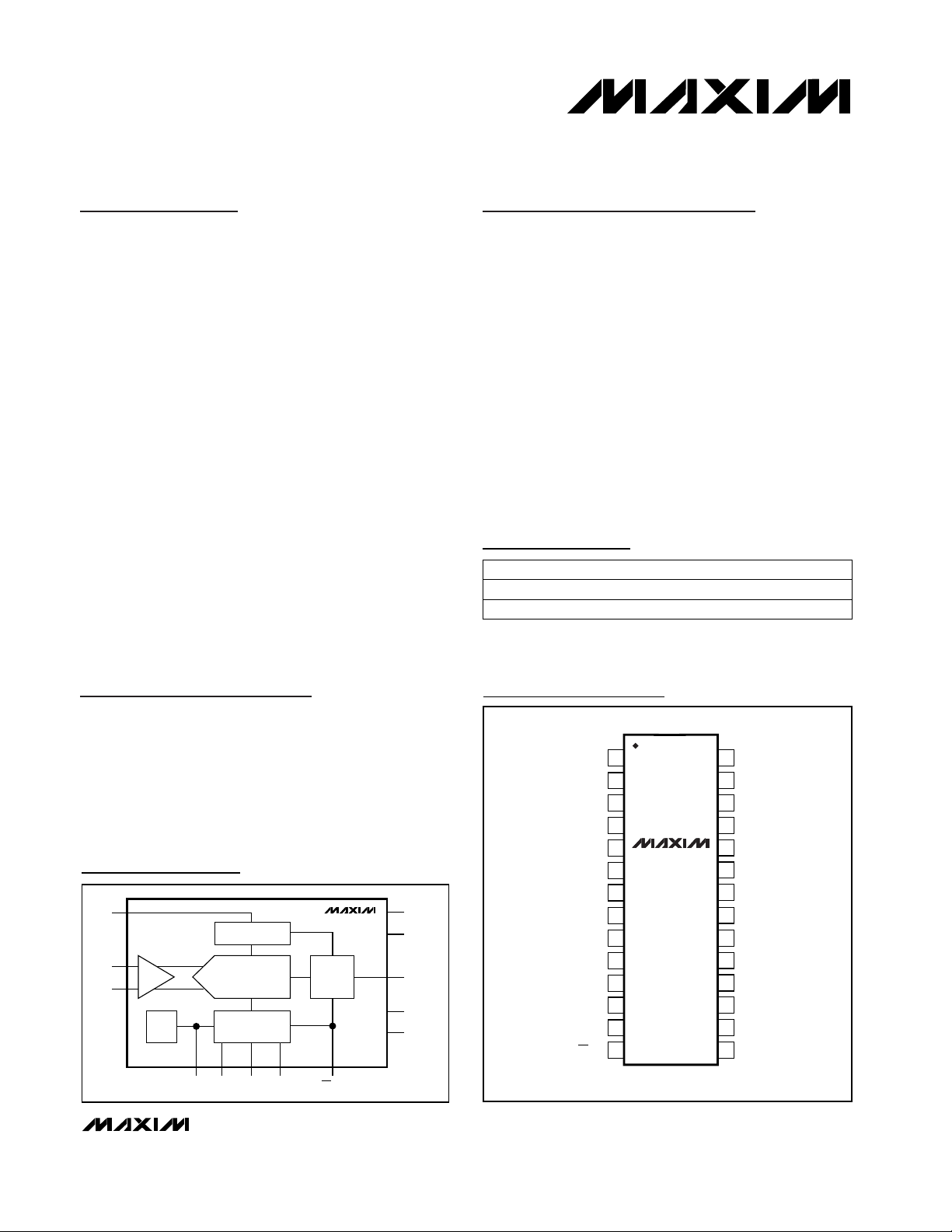
Functional Diagram
19-1597; Rev 0; 1/00
Pin Configuration
Ordering Information
PART
MAX1425CAI
MAX1425EAI -40°C to +85°C
0°C to +70°C
TEMP. RANGE PIN-PACKAGE
28 SSOP
28 SSOP
CLK
INTERFACE
INP
INN
T/H
REF
PIPELINE ADC
REF SYSTEM +
REFIN REFP CML REFN OE/PD
BIAS
AV
MAX1425
OUTPUT
DRIVERS
DD
AGND
D9–D0
DV
DD
DGND
TOP VIEW
AGND
AV
REFP
REFIN
REFN
CML
AGND
AV
INP
INN
CMLP
CMLN
CLK
OE/PD
1
2
DD
3
4
5
MAX1425
6
7
8
DD
9
10
11
12
13
14
SSOP
28
D0
27
D1
26
D2
25
D3
24
D4
23
DGND
22
DV
DD
21
DGND
20
DV
DD
19
D5
18
D6
17
D7
16
D8
15
D9
MAX1425
10-Bit, 20Msps ADC
2 _______________________________________________________________________________________
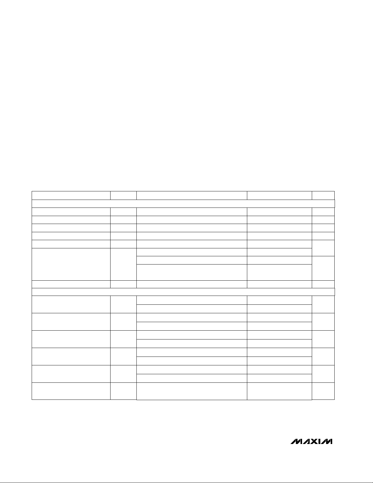
ABSOLUTE MAXIMUM RATINGS
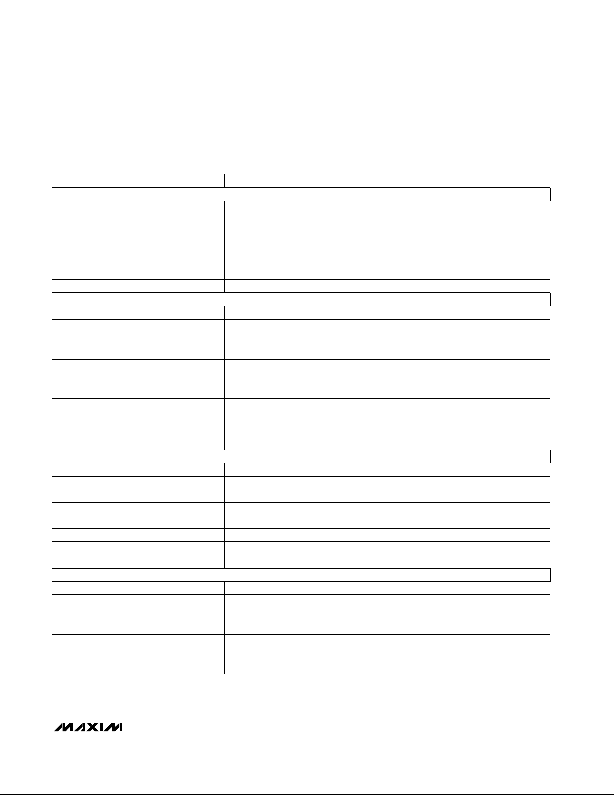
ELECTRICAL CHARACTERISTICS
(V
AV
DD
= V
CMLP
= +5V, V
DV
DD
= +3.3V, V
CMLN
= V
AGND
= V
DGND
= 0, internal reference, digital output load = 35pF, f
CLK
= 20MHz
(50% duty cycle), T
A
= T
MIN
to T
MAX
, unless otherwise noted. Typical values are at TA= +25°C.)
Stresses beyond those listed under “Absolute Maximum Ratings” may cause permanent damage to the device. These are stress ratings only, and functional
operation of the device at these or any other conditions beyond those indicated in the operational sections of the specifications is not implied. Exposure to
absolute maximum rating conditions for extended periods may affect device reliability.
AVDDto AGND ........................................................ -0.3V to +6V
DVDDto DGND ....................................................... -0.3V to +6V
AVDDto DGND........................................................ -0.3V to +6V
DGND to AGND ................................................................. ±0.3V
REFP, REFIN, REFN, CMLN, CMLP,
CML, INP, INN ....................(V
AGND
- 0.3V) to (V
AV
DD
+ 0.3V)
CLK, OE/PD, D0–D9 ...............(V
DGND
- 0.3V) to (V
DV
DD
+ 0.3V)
Continuous Power Dissipation (T
A
= +70°C)
28-Pin SSOP (derated 9.5mW/°C above +70°C) .........762mW
Operating Temperature Ranges
MAX1425CAI ..................................................... 0°C to +70°C
MAX1425EAI................................................... -40°C to +85°C
Junction Temperature..................................................... +150°C
Storage Temperature Range ............................-65°C to +150°C
Lead Temperature (soldering, 10s) .................................+300°C
SINAD
dB
PARAMETER SYMBOL MIN TYP MAX UNITS
Gain Error GE
-10 ±5 10
Midscale Offset MSO
-3 ±1.0 3
No Missing Codes
Integral Nonlinearity INL
-1.5 ±0.3 1.5
LSB
-5 ±2 5
-5 ±3 5
Power-Supply Rejection Ratio PSRR
-5 ±2 5
mV/V
Resolution RES
10
Bits
Differential Nonlinearity DNL
-1 1
LSB
Signal-to-Noise Ratio SNR
60 61
dB
Spurious-Free Dynamic Range SFDR
70 72
dB
Total Harmonic Distortion
(first five harmonics)
THD
-70 -67
dB
Signal-to-Noise and Distortion
59 61
CONDITIONS
f = 2MHz
Internal reference (Note 1)
(Note 1)
Guaranteed monotonic
External reference (REFIN) (Note 2)
External reference (REFP, CML, REFN)
(Note 3)
(Note 4)
f = 2MHz
f = 2MHz
f = 2MHz
%FSR
%FSR
f = 10MHz
56 59
f = 10MHz
64 69
f = 10MHz
-69 -64
f = 10MHz
55 59
ENOB
Bits
Effective Number of Bits
9.3 9.7
f = 2MHz
f = 10MHz
8.8 9.5
IMD
dBc
Intermodulation Distortion
-70
f1 = 10.17MHz, f2 = 10.19MHz
(-7dB FS, each tone) (Note 5)
ACCURACY
DYNAMIC PERFORMANCE (V
INP
- V
INN
= +2V to -2V)
MAX1425
10-Bit, 20Msps ADC
_______________________________________________________________________________________ 3
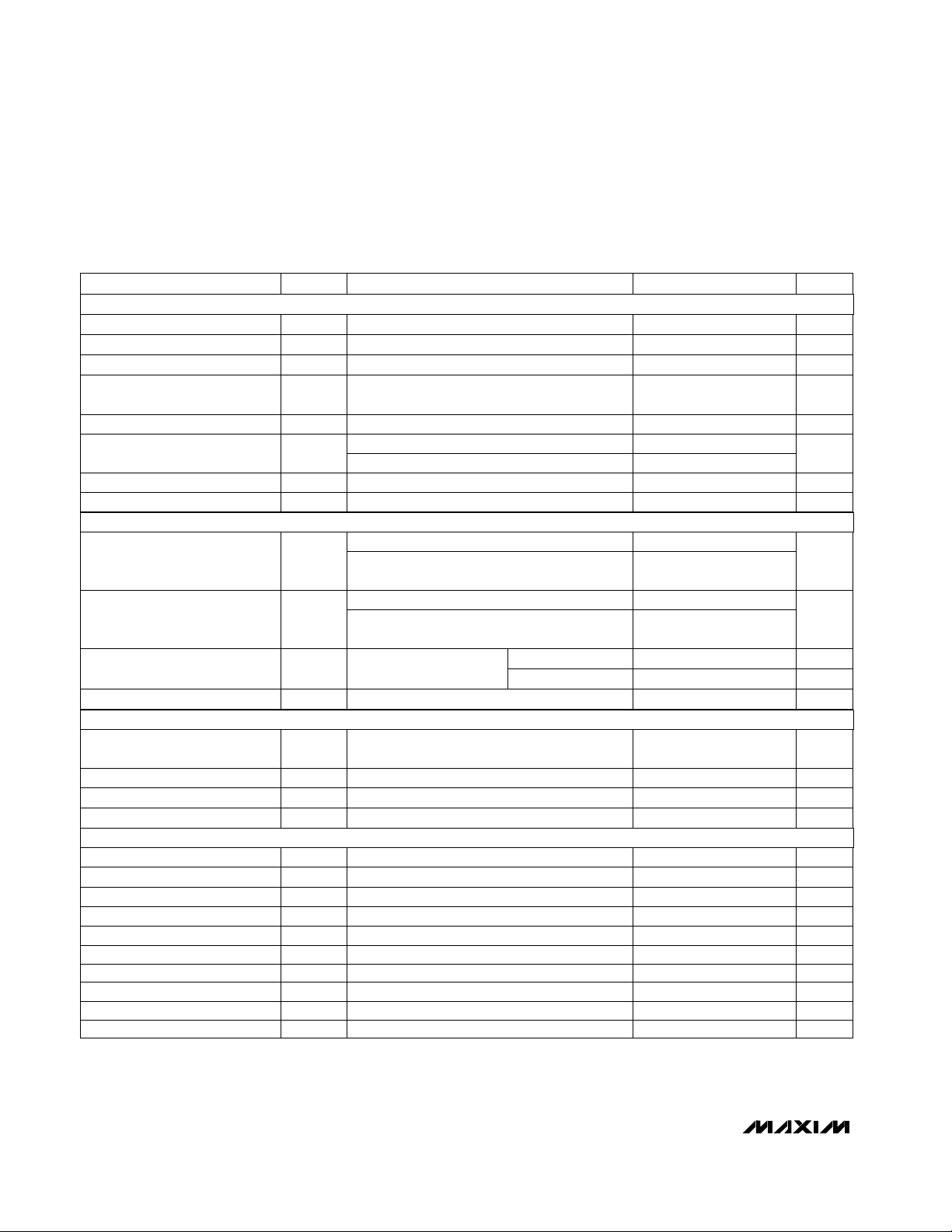
ELECTRICAL CHARACTERISTICS (continued)
(V
AV
DD
= V
CMLP
= +5V, V
DV
DD
= +3.3V, V
CMLN
= V
AGND
= V
DGND
= 0, internal reference, digital output load = 35pF, f
CLK
= 20MHz
(50% duty cycle), T
A
= T
MIN
to T
MAX
, unless otherwise noted. Typical values are at TA= +25°C.)
Common-Mode Reference
Voltage
V
CML
2.25
V(Note 1)
Differential Reference
Temperature Coefficient
±50 ppm/°C
Positive Reference Voltage V
REFP
3.25
V
Common-Mode Reference
Voltage
V
CML
2.25
V
Negative Reference Input
Voltage
V
REFN
1.25
V
Differential Reference
1.9 2.0 2.1
V
Positive Reference V
REFP
3.25
V
V
REFP
- V
REFN,TA
= +25°C
(Note 1)
Input Resistance R
IN
6.5
kΩ
Input Capacitance C
IN
10
pF
Differential Reference
2.0
V
Input Current I
IN
-325 325
µA
Input Capacitance C
IN
15
pF
REFP Input Range
3.25
±10%
V
CML Input Range
2.25
±10%
V
REFN Input Range
1.25
±10%
V
REFIN (Note 8)
REFIN
V
REFP
- V
REFN
REFP, CML, REFN
REFP, CML, REFN
Input Resistance R
IN
3.5
kΩ
Input Capacitance C
IN
8
pF
Input Common-Mode Voltage
Range
V
CMVR
2.25
±10%
V
Differential Input Range DR ±2 V
Small-Signal Bandwidth SSBW 400 MHz
Large-Signal Bandwidth LSBW 150 MHz
Either input to ground
Either input to ground
CML (Note 6)
V
INP
- V
INN
(Note 7)
(Note 7)
PARAMETER SYMBOL MIN TYP MAX UNITSCONDITIONS
Negative Reference V
REFN
1.25
V(Note 1)
Differential Reference
1.8 2 2.2
VV
REFP
- V
REFN
, TA= +25°C
Differential Reference
Temperature Coefficient
±150
ppm/°C
ANALOG INPUT (INP, INN, CML)
REFERENCE (V
REFIN
= 0; REFP, REFN, CML applied externally)
REFERENCE OUTPUTS (REFP, CML, REFN; external +2.5V reference)
REFERENCE OUTPUTS (REFP, CML, REFN; internal +2.5V reference)
MAX1425
10-Bit, 20Msps ADC
4 _______________________________________________________________________________________
ELECTRICAL CHARACTERISTICS (continued)
(V
AV
DD
= V
CMLP
= +5V, V
DV
DD
= +3.3V, V
CMLN
= V
AGND
= V
DGND
= 0, internal reference, digital output load = 35pF, f
CLK
= 20MHz
(50% duty cycle), T
A
= T
MIN
to T
MAX
, unless otherwise noted. Typical values are at TA= +25°C.)
I
OE/PD
OE/PD = DV
DD
V
DV
DD
= 5.25V, OE/PD = DV
DD
IOL= 200µA, V
DV
DD
= 2.7V
IOH= -200µA, V
DV
DD
= 2.7V
V
DV
DD
= 5.25V
V
DV
DD
< 4.75V
V
DV
DD
> 4.75V
OE/PD = DV
DD
V
DV
DD
= 5.0V
REFIN = AGND
OE/PD = DV
DD
V
DV
DD
< 4.75V
V
DV
DD
= 3.3V
V
DV
DD
> 4.75V
CONDITIONS
pF10Three-State Capacitance
µA-10 10Three-State Leakage
V0.5VOLOutput Logic Low
V
V
DV
DD
V
DV
DD
- 0.5
VOHOutput Logic High
pF10Input Capacitance
µA-20 20
µA-10 10
Input Current Leakage
0.3 ·
V
DV
DD
V
0.8
V
IL
Input Logic Low
0.7 ·
V
DV
DD
V
2.4
V
IH
Input Logic High
mW
172 220
PDPower Dissipation
µA
90 150
Digital Shutdown Current
8.5 14
mA
26 35
Analog Supply Current with
Internal Reference in Shutdown
nA
0.6 1
Analog Shutdown Current
mA
5.3 9
I
DV
DD
Digital Supply Current
UNITSMIN TYP MAXSYMBOL PARAMETER
Figure 4
Figure 4
ps7t
AJ
Aperture Jitter
ns5t
AD
Aperture Delay
cycles5.5Pipeline Delay (Latency)
ns20 25 30t
CL
Clock Low
ns20 25 30t
CH
Clock High
MHz20f
CLK
Clock Frequency
MHz0.1 20CONVConversion Rate
V
2.7 3.3 5.5
V
DV
DD
Digital Supply Voltage
V
4.75 5.00 5.25
V
AV
DD
Analog Supply Voltage
mA
31 38
I
AV
DD
Analog Supply Current
I
CLK
ns10 20t
AJ
Bus Disable
ns10 20t
AD
Bus Enable
ns52025t
OD
Data Output Delay
POWER SUPPLY
DIGITAL INPUTS (CLK, OE/PD)
DIGITAL OUTPUTS (D0–D9)
TIMING CHARACTERISTICS
MAX1425
10-Bit, 20Msps ADC
_______________________________________________________________________________________ 5
ELECTRICAL CHARACTERISTICS (continued)
Note 1: Internal reference, REFIN bypassed to AGND with a 0.1µF capacitor.
Note 2: External +2.5V reference applied to REFIN.
Note 3: Internal reference disabled. V
REFIN
= 0, V
REFP
= 3.25V, V
CML
= 2.25V, and V
REFN
= 1.25V.
Note 4: Measured as the ratio of the change in midscale offset voltage for a ±5% change in V
AV
DD
using the internal reference.
Note 5: IMD is measured with respect to either of the fundamental tones.
Note 6: Specifies the common-mode range of the differential input signal supplied to the MAX1425.
Note 7: Defined as the input frequency at which the fundamental component of the output spectrum is attenuated by 3dB.
Note 8: V
REFIN
is internally biased to +2.5V through a 5kΩ resistor.
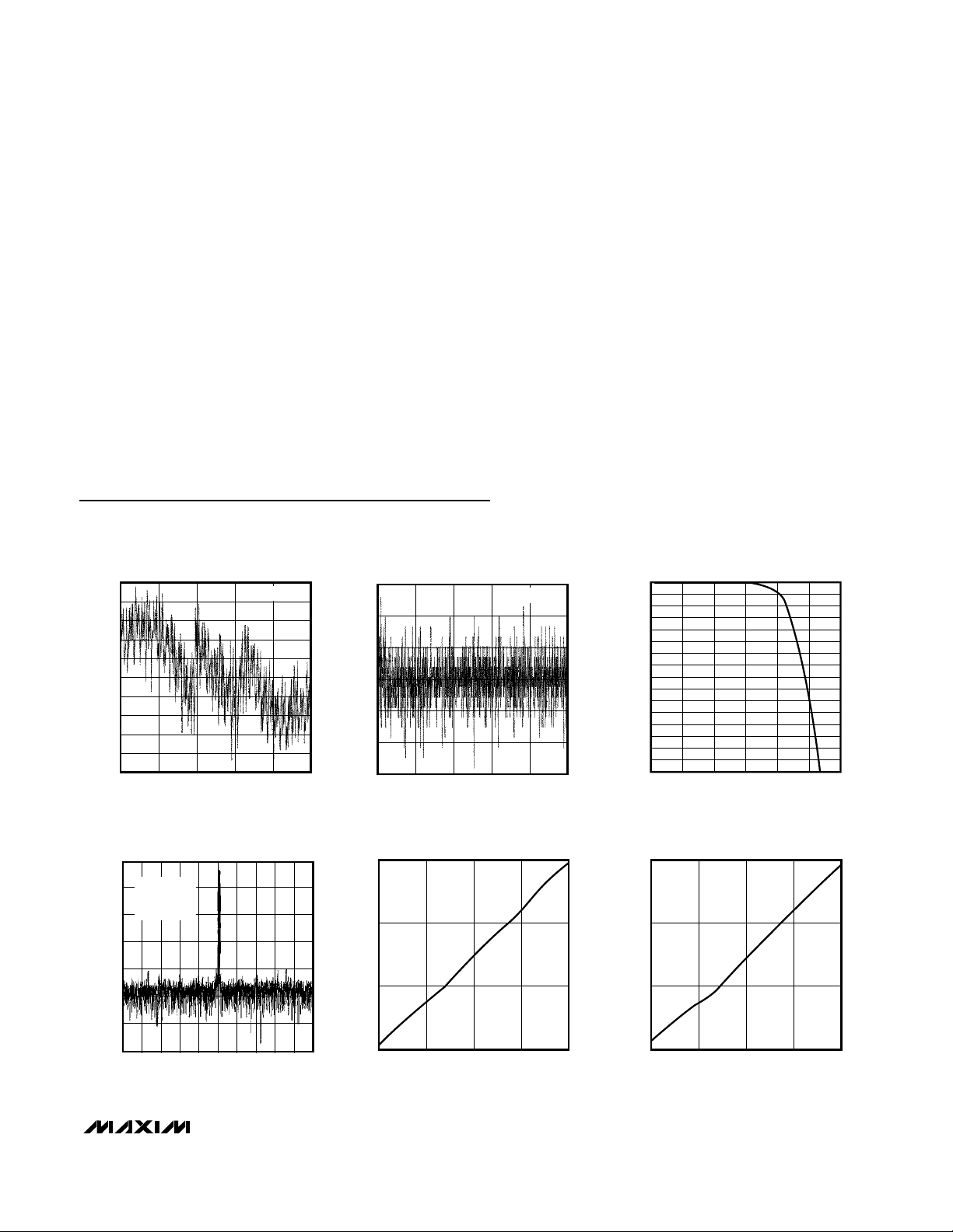
Typical Operating Characteristics
(V
AV
DD
= V
CMLP
= +5V, V
DV
DD
= +3.3V, V
CMLN
= V
AGND
= 0, internal reference, digital output load = 35pF, f
CLK
= 20Msps (50%
duty cycle), for dynamic performance 0dB is full scale, T
A
= +25°C, unless otherwise noted.)
-1.2
-0.6
-0.8
-1.0
-0.4
-0.2
0
0.2
0.4
0.6
0.8
0 400200 600
800
1000
INTEGRAL NONLINEARITY vs. CODE
MAX1425-01
CODE
INL (LSB)
f
INP
= 2MHz
-0.6
-0.2
-0.4
0
0.2
0.4
0.6
0 400200 600
800
1000
DIFFERENTIAL NONLINEARITY vs. CODE
MAX1425-02
CODE
DNL (LSB)
f
INP
= 2MHz
-8.0
-6.0
-7.0
-5.0
-4.0
-3.0
-2.0
-1.0
0
0.01 10.1 10 100 1000 10,000
ANALOG INPUT BANDWIDTH
(FULL POWER)
MAX1425-03
BANDWIDTH (MHz)
AMPLITUDE (dB)
-140
-100
-120
-60
-80
-20
-40
0
042681537910
INTERMODULATION DISTORTION
vs. FREQUENCY
MAX1425-04
FREQUENCY (MHz)
MAGNITUDE (dB)
f
CLK
= 20MHz
f1 = 5.01MHz
f2 = 5.03MHz
f
CLK
= 20MHz
f1 = 5.01MHz
f2 = 5.03MHz
0
20
40
60
SIGNAL-TO-NOISE PLUS DISTORTION
vs. POWER (f
IN
= 2.003MHz)
MAX1425-05
INPUT (dB)
SINAD (dB)
-60 -30-45 -15 0
0
20
40
60
SIGNAL-TO-NOISE RATIO PLUS DISTORTION
vs. POWER (f
IN
= 5.009MHz)
MAX1425-06
INPUT (dB)
SNDR (dB)
-60 -30-45 -15 0
 Loading...