

General Description
The MAX1407/MAX1408/MAX1409/MAX1414 are lowpower, general-purpose, multichannel data-acquisition
systems (DAS). These devices are optimized for lowpower applications. All the devices operate from a single +2.7V to +3.6V power supply and consume a
maximum of 1.15mA in Run mode and only 2.5µA in
Sleep mode.
The MAX1407/MAX1408/MAX1414 feature a differential
8:1 input multiplexer to the ADC, a programmable
three-state digital output, an output to shutdown an
external power supply, and a data ready output from
the ADC. The MAX1408 has eight auxiliary analog
inputs, while the MAX1407/MAX1414 include four auxiliary analog inputs and two 10-bit force/sense DACs.
The MAX1414 features a 50mV trip threshold for the
signal-detect comparator while the others have a 0mV
trip threshold. The MAX1409 is a 20-pin version of the
DAS family with a differential 4:1 input multiplexer to the
ADC, one auxiliary analog input, and one 10-bit
force/sense DAC.
The MAX1407/MAX1408/MAX1414 are available in
space-saving 28-pin SSOP packages, while the
MAX1409 is available in a 20-pin SSOP package.
Applications
Medical Instruments
Industrial Control Systems
Portable Equipment
Data-Acquisition System
Automatic Testing
Robotics
Features
♦ +2.7V to +3.6V Supply Voltage Range in Standby,
Idle, and Run Mode (Down to 1.8V in Sleep Mode)
♦ 1.15mA Run Mode Supply Current
♦ 2.5µA Sleep Mode Supply Current (Wake-Up, RTC,
and Voltage Monitor Active)
♦ Multichannel 16-Bit Sigma-Delta ADC
±1.5 LSB (typ) Integral Nonlinearity
30Hz or 60Hz Continuous Conversion Rate
Buffered or Unbuffered Mode
Gain of +1/3, +1, or +2V/V
Unipolar or Bipolar Mode
On-Chip Offset Calibration
♦ 10-Bit Force/Sense DACs
♦ Buffered 1.25V, 18ppm/°C (typ) Bandgap
Reference Output
♦ SPI™/QSPI™ or MICROWIRE™-Compatible Serial
Interface
♦ System Support Functions
RTC (Valid til 9999) and Alarm
High-Frequency PLL Clock Output (2.4576MHz)
+1.8V and +2.7V RESET and Power-Supply
Voltage Monitors
Signal Detect Comparator
Interrupt Generator (INT and DRDY)
Three-State Digital Output
Wake-Up Circuitry
♦ 28-Pin SSOP (MAX1407/MAX1408/MAX1414),
20-Pin SSOP (MAX1409)
MAX1407/MAX1408/MAX1409/MAX1414
Low-Power, 16-Bit Multichannel DAS with
Internal Reference,10-Bit DACs, and RTC
________________________________________________________________ Maxim Integrated Products 1
19-2229; Rev 0; 10/01
Pin Configurations continued at end of data sheet.
Typical Operating Circuit appears at end of data sheet.
SPI and QSPI are trademarks of Motorola, Inc.
MICROWIRE is a trademark of National Semiconductor Corp.
Ordering Information
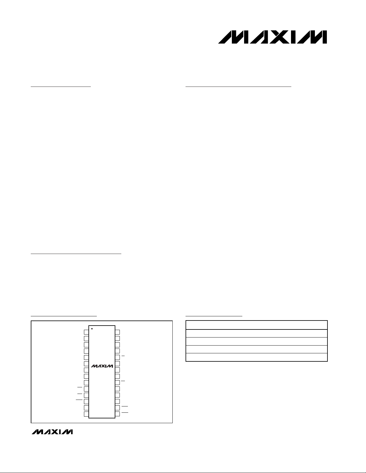
Pin Configurations
For pricing, delivery, and ordering information, please contact Maxim/Dallas Direct! at
1-888-629-4642, or visit Maxim’s website at www.maxim-ic.com.
TOP VIEW
FB2
FB1
OUT1
REF
AGND
AV
CPLL
WU1
WU2
RESET
1
2
DO
3
4
5
IN0
6
7
MAX1407
MAX1414
8
DD
9
10
11
12
13
IN1
14
IN2
28
OUT2
27
IN3
26
DV
DD
25
DGND
24
CS
23
SCLK
22
DIN
21
DOUT
20
INT
19
CLKIN
18
CLKOUT
17
FOUT
16
DRDY
15
SHDN
PART TEMP. RANGE PIN-PACKAGE
MAX1407CAI 0°C to +70°C 28 SSOP
MAX1408CAI 0°C to +70°C 28 SSOP
MAX1409CAP 0°C to +70°C 20 SSOP
MAX1414CAI 0°C to +70°C 28 SSOP
MAX1407/MAX1408/MAX1409/MAX1414
Low-Power, 16-Bit Multichannel DAS with
Internal Reference,10-Bit DACs, and RTC
2 _______________________________________________________________________________________
ABSOLUTE MAXIMUM RATINGS
Stresses beyond those listed under “Absolute Maximum Ratings” may cause permanent damage to the device. These are stress ratings only, and functional
operation of the device at these or any other conditions beyond those indicated in the operational sections of the specifications is not implied. Exposure to
absolute maximum rating conditions for extended periods may affect device reliability.
AVDDto AGND .........................................................-0.3V to +6V
AV
DD
to DVDD...................................................... -0.3V to +0.3V
Analog Inputs to AGND .........................-0.3V to +(AV
DD
+ 0.3V)
Digital Inputs to DGND.............................................-0.3V to +6V
Maximum Current Input Into Any Pin ..................................50mA
Continuous Power Dissipation (T
A
= +70°C)
20-Pin SSOP (derate 8.0mW/°C above +70°C) ...........640mW
28-Pin SSOP (derate 9.52mW/°C above +70°C) .........762mW
DV
DD
to DGND.........................................................-0.3V to +6V
AGND to DGND.....................................................-0.3V to +0.3V
Analog Outputs to AGND ......................-0.3V to +(AV
DD
+ 0.3V)
Digital Outputs to DGND .......................-0.3V to +(AV
DD
+ 0.3V)
REF to AGND.........................................-0.3V to +(AV
DD
+ 0.3V)
Operating Temperature Range:
MAX14__CA_ ......................................................0°C to +70°C
MAX14__EA_ ...................................................-40°C to +85°C
Lead Temperature (soldering, 10s) ................................+300 °C
Storage Temperature Range .............................-65°C to +150°C
Junction Temperature......................................................+150°C
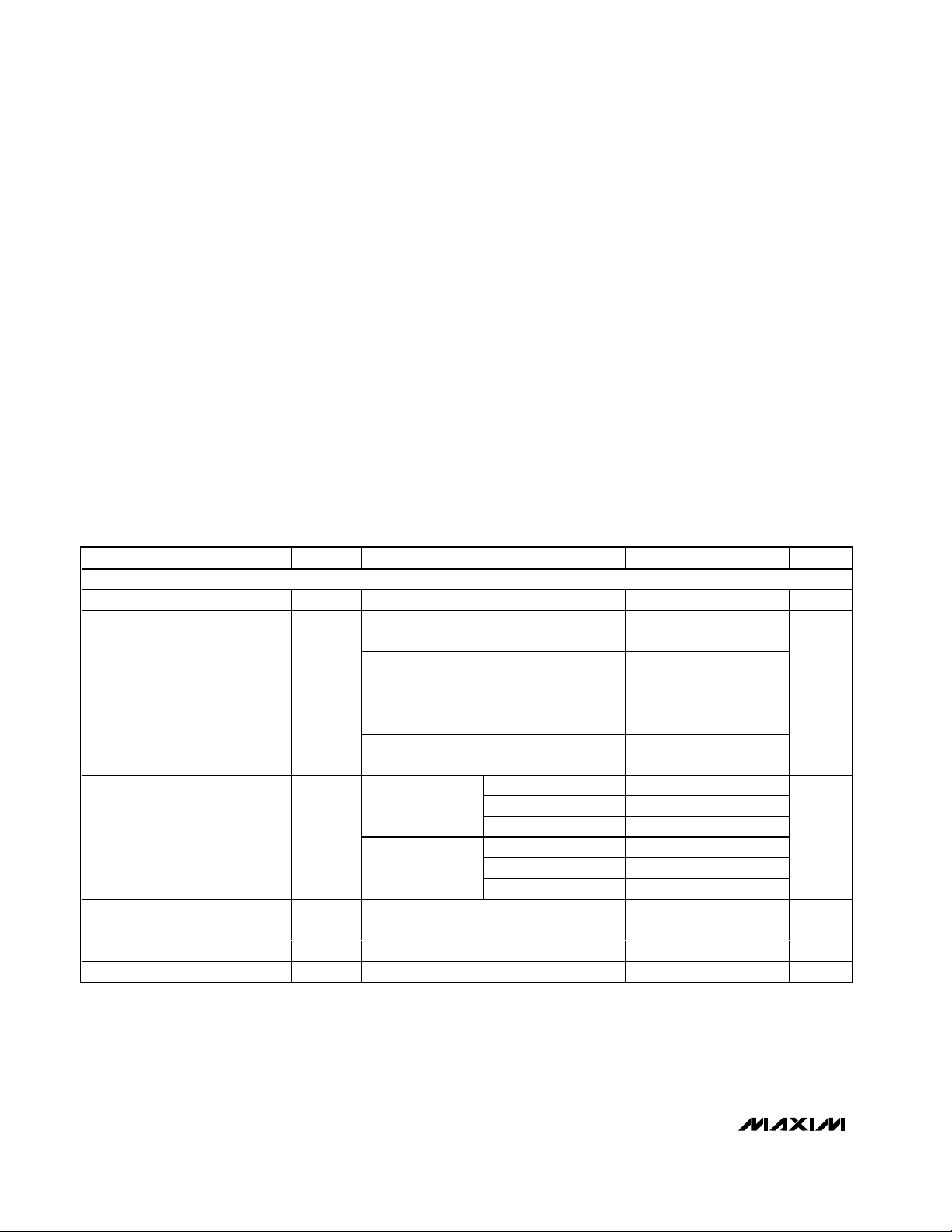
ELECTRICAL CHARACTERISTICS
(DVDD= AVDD= +2.7V to 3.6V, 4.7µF at REF, internal V
REF
, 18nF between CPLL and AVDD, 32.768kHz crystal across CLKIN and
CLKOUT, T
A
= T
MIN
to T
MAX
, unless otherwise noted. Typical values are at TA= +25°C.)
ADC ACCURACY
Resolution (No Missing Codes) RES 16 Bits
Integral Nonlinearity INL
Output RMS Noise (Note 1)
Offset Error On-chip calibration removes this error ±1 % of FS R
Offset Drift ±0.5 µV/°C
Gain Error Excludes offset and reference errors ±1 % of FS R
Gain Drift Excludes offset and reference errors ±1 p p m /° C
PARAMETER SYMBOL CONDITIONS MIN TYP MAX U N I T S
Unbuffered mode, Unipolar mode, gain = 1,
V
NEG
U nb uffer ed m od e, U ni p ol ar m od e, g ai n = 2,
V
N E G
Unbuffered mode, Bipolar mode, gain = 1,
V
NEG
Buffered mode, Bipolar mode, gain = 2,
V
NEG
Unipolar
Bipolar Mode
= 0.2V, fully differential input (Note 7)
= 0.625V , p seud o- d i ffer enti al i np ut
= 0.625V, fully differential input
= 0.625V, fully differential input
1.5 3.5
1.75
1.70
2.50
Gain = 2 ±5
Gain = 1 ±10
Gain = 1/3 ±30
Gain = 2 ±8
Gain = 1 ±16.5
Gain = 1/3 ±48.5
LSB
µV
RMS
MAX1407/MAX1408/MAX1409/MAX1414
Low-Power, 16-Bit Multichannel DAS with
Internal Reference,10-Bit DACs, and RTC
_______________________________________________________________________________________ 3
ELECTRICAL CHARACTERISTICS (continued)
(DVDD= AVDD= +2.7V to 3.6V, 4.7µF at REF, internal V
REF
, 18nF between CPLL and AVDD, 32.768kHz crystal across CLKIN and
CLKOUT, T
A
= T
MIN
to T
MAX
, unless otherwise noted. Typical values are at TA= +25°C.)
Power-Supply Rejection Ratio Gain = 1, unipolar and buffered mode 70 dB
Output Update Rate
Turn-On Time Excluding reference 50 µs
SIGNAL DETECT COMPARATOR
Differential Input-Detection
Threshold Voltage
Common-Mode Input Voltage
Turn-On Time 10 µs
ANALOG INPUTS
Differential Input Voltage Range
Absolute Input Voltage Range
Common-Mode Input Voltage
Range
Common-Mode Rejection Ratio Gain = 1, unipolar and buffered mode 90 dB
Input Sampling Rate FOUT = 2.4576MHz
Input Current Buffered mode ±0.5 nA
Input Capacitance 15 pF
F O R C E- SEN SE D A C ( al l m easur em ents m ad e w i th FB1( 2) shor ted to O U T1( 2) , unl ess other w i se noted ) .
( M AX 1407/M AX 1409/M AX 1414 onl y)
Resolution 10 Bits
Differential Nonlinearity Guaranteed monotonic (Note 2) ±1.0 LSB
Integral Nonlinearity (Note 2) ±1.0 LSB
Offset Error (Note 3) ±20 mV
Offset Drift ±5 µV/°C
Gain Error Excludes offset and reference drift 3.6 mV
Gain Drift Excludes offset and reference drift 10 ppm/°C
Line Regulation 190 µV/V
Current into FB1(2) ±0.5 nA
PARAMETER SYMBOL CONDITIONS MIN TYP MAX U N I T S
Continuous
conversion
MAX1407/MAX1408/MAX1409 -10 0 10
MAX1414 44 50 56
Unipolar mode
Bipolar mode
Unbuffered -0.05 AV
Buffered 0.05 1.40
Unbuffered AGND AV
Buffered 0.05 1.40
1/3
1PGA Gain See PGA Gain section
2
RATE bit = 0 30
RATE bit = 1 60
0 0.8 V
ADC gain = 1 0 V
ADC gain = 2 0 V
ADC gain = 1/3 0 AV
ADC gain = 1 -V
ADC gain = 2 -V
ADC gain = 1/3 -AV
30Hz data rate 15.360
60Hz data rate 30.720
REF
REF/2
DD
REF/2
V
V
REF/2
AV
REF
DD
REF
DD
DD
DD
kHz
V/V
Hz
mV
V
V
V
MAX1407/MAX1408/MAX1409/MAX1414
Low-Power, 16-Bit Multichannel DAS with
Internal Reference,10-Bit DACs, and RTC
4 _______________________________________________________________________________________
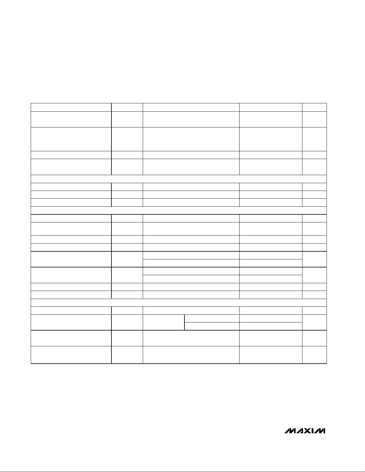
ELECTRICAL CHARACTERISTICS (continued)
(DVDD= AVDD= +2.7V to 3.6V, 4.7µF at REF, internal V
REF
, 18nF between CPLL and AVDD, 32.768kHz crystal across CLKIN and
CLKOUT, T
A
= T
MIN
to T
MAX
, unless otherwise noted. Typical values are at TA= +25°C.)
Output Slew Rate
Output Settling Time
Turn-On Time 100 µs
OUT1, OUT2 Output Range No Load (Note 4) 0.05
EXTERNAL REFERENCE (internal reference powered down)
Input Voltage Range 1.25 ±0.10 V
Input Resistance 540 kΩ
Input Current 2.3 µA
INTERNAL REFERENCE (AVDD = 3V, unless otherwise noted)
Output Voltage TA = +25°C 1.225 1.25 1.275 V
Output Voltage Temperature
Coefficient
Output Short-Circuit Current 3.4 mA
Line Regulation ∆V
Load Regulation
Noise Voltage e
Power-Supply Rejection Ratio ±100mV, f = 120Hz 70 dB
Turn-On Time 3ms
µP RESET
Supply Voltage Range For valid RESET 1 3.6 V
RESET Trip Threshold Low V
Low AVDD Trip Threshold
RESET Output Low Voltage
(Open-Drain Output)
PARAMETER SYMBOL CONDITIONS MIN TYP MAX U N I T S
010hex to 3FFhex and 3FFhex to 010hex
cod e sw i ng , R
To ±1/2 LSB (at 10-bit accuracy) of fullscale with code transition from 010hex
to 3FFhex, R
/∆V DD2.7<AVDD<3.6V 80 µV/V
RE F
I
SOURCE
I
SINK
OUT
TH
0.1Hz to 10Hz 40
10Hz to 10kHz 400
AVDD falling
For Normal, Idle, and Standby modes,
AV
I
SINK
= 12kΩ , C L = 200p F
L
= 12kΩ, CL = 200pF
L
= 0µA to 500µA, TA = +25°C1
= 0µA to 50µA, TA = +25°C2
Bit VM = 1 1.800 1.865 1.930
Bit VM = 0 2.70 2.75 2.80
falling
DD
= 1mA, AVDD = 1.8V 0.4 V
2.70 2.75 2.80 V
18.0 V/ms
65 µs
AV
DD
- 0.2
18 p p m /° C
V
µV/µA
µVp-p
V
MAX1407/MAX1408/MAX1409/MAX1414
Low-Power, 16-Bit Multichannel DAS with
Internal Reference,10-Bit DACs, and RTC
_______________________________________________________________________________________ 5
ELECTRICAL CHARACTERISTICS (continued)
(DVDD= AVDD= +2.7V to 3.6V, 4.7µF at REF, internal V
REF
, 18nF between CPLL and AVDD, 32.768kHz crystal across CLKIN and
CLKOUT, T
A
= T
MIN
to T
MAX
, unless otherwise noted. Typical values are at TA= +25°C.)
RESET Output Leakage AVDD > VTH, RESET deasserted 0.002 0.1 µA
Turn-On Time 2ms
CRYSTAL OSCILLATOR
Crystal Frequency AVDD = +3V 32.768 kHz
Crystal Load Capacitance 6pF
Oscillator Stability AV
Oscillator Startup Time 1.5 s
PLL
FOUT Frequency AVDD = +3V 2.4576 MHz
Absolute Clock Jitter Cycle-to-cycle 10 ns
Frequency Tolerance/Stability
FOUT Rise/Fall Time 20% to 80% waveform, CL = 30pF 15 30 ns
Duty Cycle 40 50 60 %
DIGITAL INPUTS (DIN, SCLK, CS, WU1, WU2)
Input High Voltage DVDD = +1.8V to +3.6V
Input Low Voltage DVDD = +1.8V to +3.6V
Input Hysteresis DVDD = +3V 200 mV
DIN, SCLK, CS, Input Current VIN = 0 or VIN = DV
WU1, WU2 Input Current VIN = AV
WU1, WU2 Pullup Current VIN = 0 10 µA
Input Capacitance 10 pF
DIGITAL OUTPUTS (DOUT, FOUT, INT, DRDY, SHDN, D0)
DOUT, FOUT, DRDY, INT
Output Low Voltage
DOUT, FOUT, DRDY, INT,
SHDN Output High Voltage
DOUT Three-State Leakage ±0.01 ±10 µA
DOUT Three-State Capacitance 15 pF
SHDN Output Low Voltage
(MAX1407/MAX1408/MAX1414
only)
PARAMETER SYMBOL CONDITIONS MIN TYP MAX U N I T S
D D
Overtemperature excluding crystal,
T
= T
A
Over supp l y vol tag e, + 2.7V < AV
V
OL
V
OH
I
SINK
I
SOURCE
I
SINK
I
SINK
= + 1.8V to + 3.6V , excl ud i ng cr ystal 0 ppm/V
to T
MIN
MAX
< +3.6V 0 p p m /m V
D D
0.7 x
DV
DD
DD
DD
= 1mA, DVDD = +1.8V to +3.6V 0.4 V
= 0.2mA, DVDD = +1.8V to +3.6V 0.8 x DV
= 1mA, DVDD = +1.8V to +3.6V 0.4
= 50µA, DVDD = +1.8V to +3.6V
0p p m /° C
0.3 x
DV
DD
±0.01 ±10 µA
0.01 10 µA
DD
0.04 x
DV
DD
V
V
V
V
MAX1407/MAX1408/MAX1409/MAX1414
Low-Power, 16-Bit Multichannel DAS with
Internal Reference,10-Bit DACs, and RTC
6 _______________________________________________________________________________________
ELECTRICAL CHARACTERISTICS (continued)
(DVDD= AVDD= +2.7V to 3.6V, 4.7µF at REF, internal V
REF
, 18nF between CPLL and AVDD, 32.768kHz crystal across CLKIN and
CLKOUT, T
A
= T
MIN
to T
MAX
, unless otherwise noted. Typical values are at TA= +25°C.)
TIMING CHARACTERISTICS
(MAX1407/MAX1408/MAX1409/MAX1414: AV
DD
= DV
DD
= 2.7V to 3.6V, TA = T
MIN
to T
MAX,
unless otherwise noted.)
D0 Output Low Voltage
(MAX1407/MAX1408/MAX1414
only)
PARAMETER SYMBOL CONDITIONS MIN TYP MAX U N I T S
I
SINK
= 200µA, DVDD = +2.7V to +3.6V 0.7 mV
D0 Output High Voltage
(MAX1407/MAX1408/MAX1414
only)
POWER REQUIREMENTS
Supply Voltage Range V
Supply Current (Note 5) I
DD
DD
= 2m A, D V
I
S OU RC E
Run, Idle, and Standby mode 2.7 3.6
Sleep mode 1.8 3.6
Run mode
Standby mode
Sleep mode
V
= 2.7V
DD
= + 2.7V to + 3.6V
D D
MAX1407/MAX1414 1.15
MAX1408 1.03
MAX1409 1.09
MAX1407/MAX1414 650
MAX1408 530Idle mode
MAX1409 590
MAX1407/MAX1408/
MAX1409/MAX1414
MAX1407/MAX1408/
MAX1409/MAX1414
DV
- 0.1
DD
TIMING PARAMETERS
SCLK Operating Frequency f
SCLK Cycle Time t
SCLK Pulse Width High t
SCLK Pulse Width Low t
DIN to SCLK Setup t
DIN to SCLK Hold t
SCLK Fall to Output Data Valid t
CS Fall to Output Enable t
CS Rise to Output Disable t
CS to SCLK Rise Setup t
CS to SCLK Rise Hold t
PARAMETER SYMBOL CONDITIONS MIN TYP MAX UNITS
SCLK
CYC
CSS
CSH
CH
CL
DS
DH
DO
DV
TR
CL = 50pF (see load circuit) 200 ns
CL = 50pF (see load circuit) 240 ns
CL = 50pF (see load circuit) 240 ns
476 ns
190 ns
190 ns
100 ns
0ns
100 ns
0ns
330
1.7 2.5
V
V
mA
µA
2.1 MHz
MAX1407/MAX1408/MAX1409/MAX1414
Low-Power, 16-Bit Multichannel DAS with
Internal Reference,10-Bit DACs, and RTC
_______________________________________________________________________________________ 7
Note 1: Single conversion.
Note 2: DNL and INL are measured between code 010hex and 3FFhex.
Note 3: Offset error is referenced to code 010hex.
Note 4: Output swing is a function of external gain-setting feedback resistors and REF voltage.
Note 5: Measured with no load on FOUT, DOUT, and the DAC amplifiers. SCLK is idle, and all digital inputs are at DGND or DV
DD
.
Note 6: SHDN stays high if the PLL is on.
Note 7: Actual worst-case performance is ±2.5LSB. Guaranteed limit of ±3.5LSB is due to production test limitation.
Note 8: Guaranteed by design. Not production tested.
TIMING CHARACTERISTICS (continued)
(MAX1407/MAX1408/MAX1409/MAX1414: AV
DD
= DV
DD
= 2.7V to 3.6V, TA = T
MIN
to T
MAX,
unless otherwise noted.)
TYPICAL TIMING PARAMETERS
OUT1/OUT2 Turn-Off Time
Sleep Voltage Monitor Timeout
Period
WU1 or WU2 Pulse Width t
Shutdown Deassert Delay t
FOUT Turn-On Time t
PARAMETER SYMBOL CONDITIONS MIN TYP MAX UNITS
t
DSLP
WU
DPU
DFON
Input impedance > 1MΩ
(MAX1407/MAX1409/MAX1414 only)
The delay for the sleep voltage monitor
output, RESET, to go high after AV
above the reset threshold (+1.8V when bit
VM = 1 and +2.7V, when bit VM = 0); this is
largely driven by the startup of the 32kHz
oscillator
Minimum pulse width required to detect a
wake-up event
The delay for SHDN to go high after a valid
wake-up event
The turn-on time for the high-frequency
clock; it is gated by an AND function with
three signals—the RESET signal, the internal
low voltage V
assertion of the PLL; the time delay is timed
from when the low-voltage monitor trips or
the RESET going high, whichever happens
later; FOUT always starts in the low state
monitor signal, and the
DD
DD
rises
100 µs
1.54 s
1µs
1µs
31.25 ms
The delay for INT to go low after the FOUT
INT Delay t
FOUT Disable Delay t
SHDN Assertion Delay t
DFI
DFOF
DPD
clock output has been enabled; INT is used
as an interrupt signal to inform the µP the
high-frequency clock has started
The delay after a shutdown command has
asserted and before FOUT is disabled; this
gives the microcontroller time to clean up
and go into Sleep mode properly
The delay after a shutdown command has
asserted and before SHDN is pulled low
(turning off the DC-DC converter) (Note 6)
7.82 ms
1.95 ms
2.93 ms
MAX1407/MAX1408/MAX1409/MAX1414
Low-Power, 16-Bit Multichannel DAS with
Internal Reference,10-Bit DACs, and RTC
8 _______________________________________________________________________________________
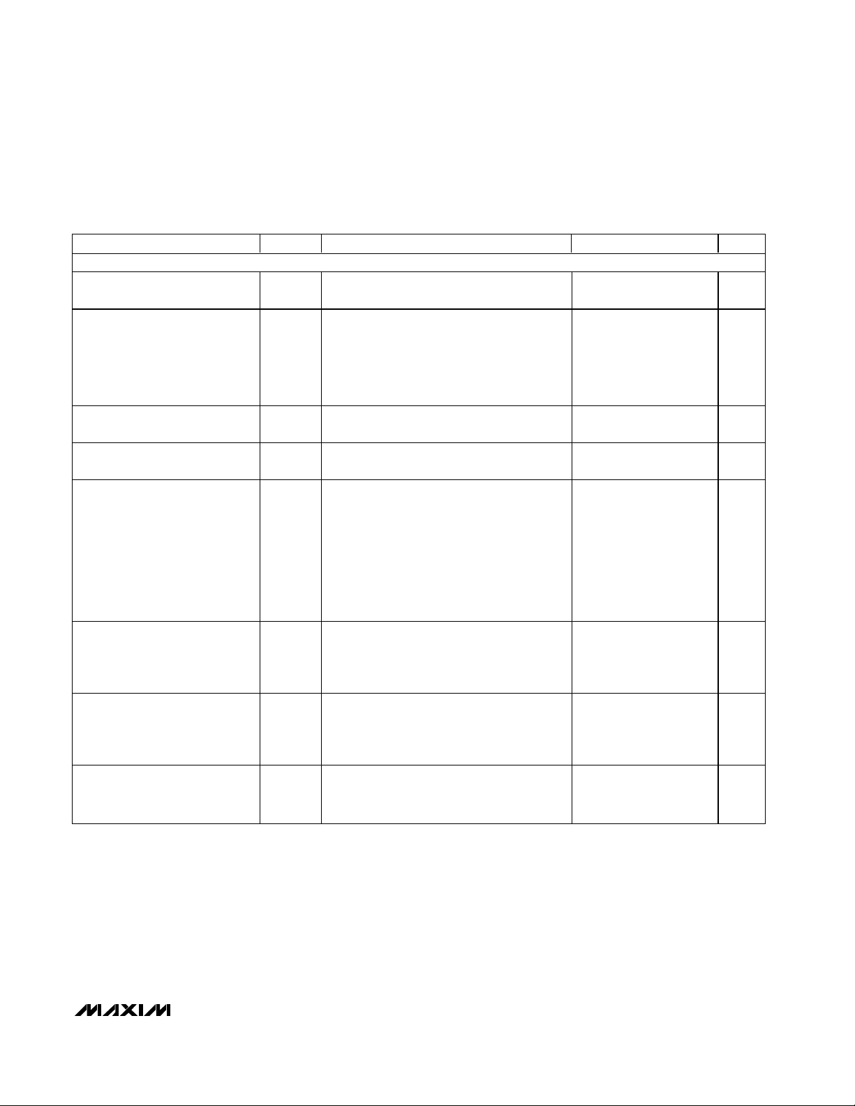
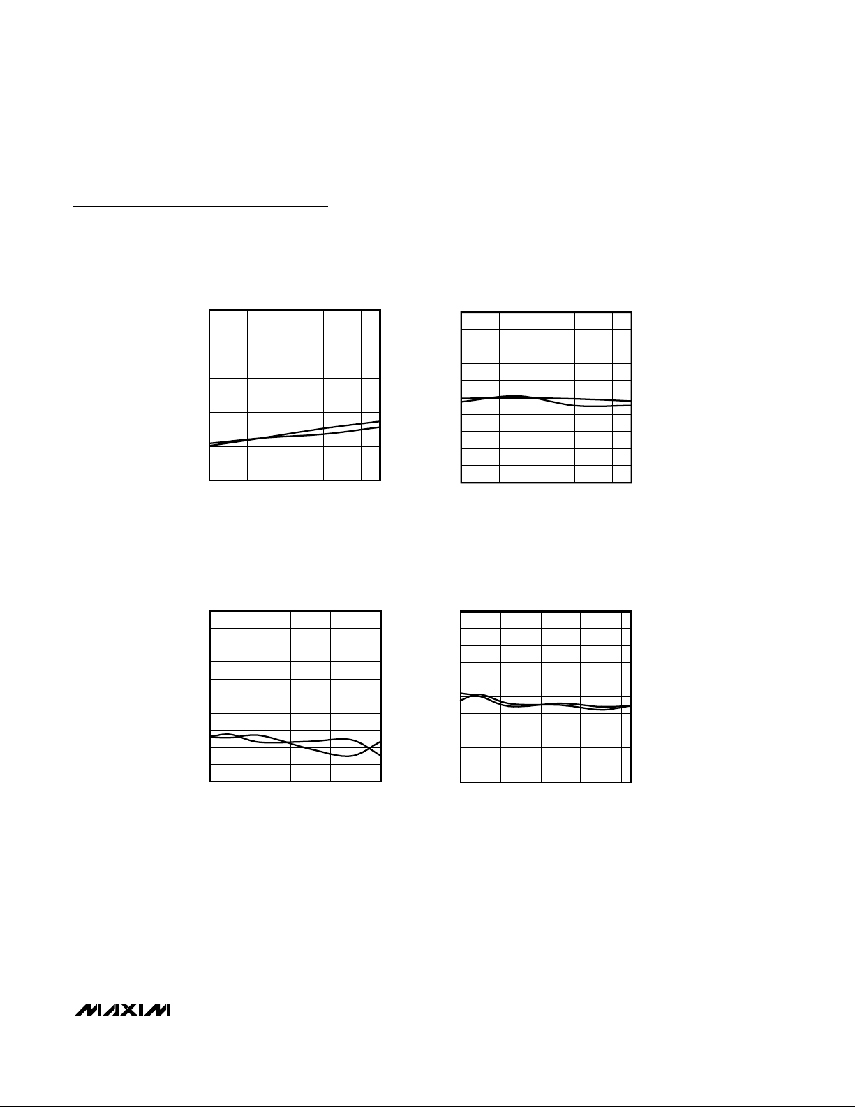
Typical Operating Characteristics
(A
VDD
= D
VDD
= 3V, MAX1407 used, TA = +25°C, unless otherwise noted.)
0
200
100
400
300
600
500
700
2.70 3.00 3.152.85 3.30 3.45 3.60
SUPPLY CURRENT vs.
SUPPLY VOLTAGE
MAX1407 toc01
SUPPLY VOLTAGE (V)
SUPPLY CURRENT (µA)
RUN MODE
IDLE MODE
STANDBY
0
200
100
400
300
600
500
700
-40
10 35-15 60 85
SUPPLY CURRENT vs.
TEMPERATURE
MAX1407 toc02
TEMPERATURE (°C)
SUPPLY CURRENT (µA)
STANDBY
IDLE MODE
RUN MODE
1.0
2.0
1.5
3.0
2.5
3.5
4.0
1.80 2.802.30 3.30
SLEEP CURRENT vs. FALLING V
DD
MAX1407 toc03
SUPLLY VOLTAGE (V)
SLEEP CURRENT (µA)
0
1.0
0.5
2.0
1.5
2.5
3.0
-40 10-15 35 60 85
SLEEP MODE SUPPLY CURRENT
vs. TEMPERATURE
MAX1407 toc04
TEMPERATURE (°C)
SUPPLY CURRENT (µA)
Load Circuits
DV
DD
DV
DD
DOUT
6kΩ
DOUT
C
6kΩ
DGND
a) VOH TO HIGH-Z
LOAD
50pF
b) V
LOAD CIRCUITS FOR DISABLE TIME
TO HIGH-Z
OL
C
LOAD
50pF
DGND
6kΩ
DOUT
6kΩ
DGND
a) HIGH-Z TO VOH AND VOL TO V
LOAD CIRCUITS FOR ENABLE TIME
C
50pF
DOUT
LOAD
b) HIGH-Z TO VOL AND VOH TO V
OH
C
LOAD
50pF
DGND
OL
MAX1407/MAX1408/MAX1409/MAX1414
Low-Power, 16-Bit Multichannel DAS with
Internal Reference,10-Bit DACs, and RTC
_______________________________________________________________________________________ 9
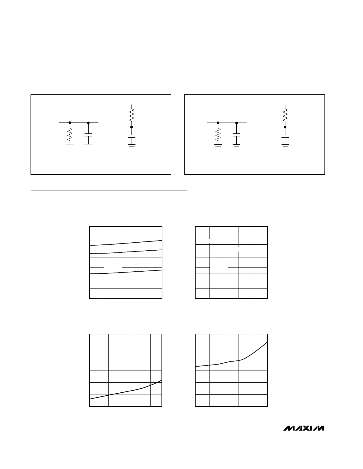
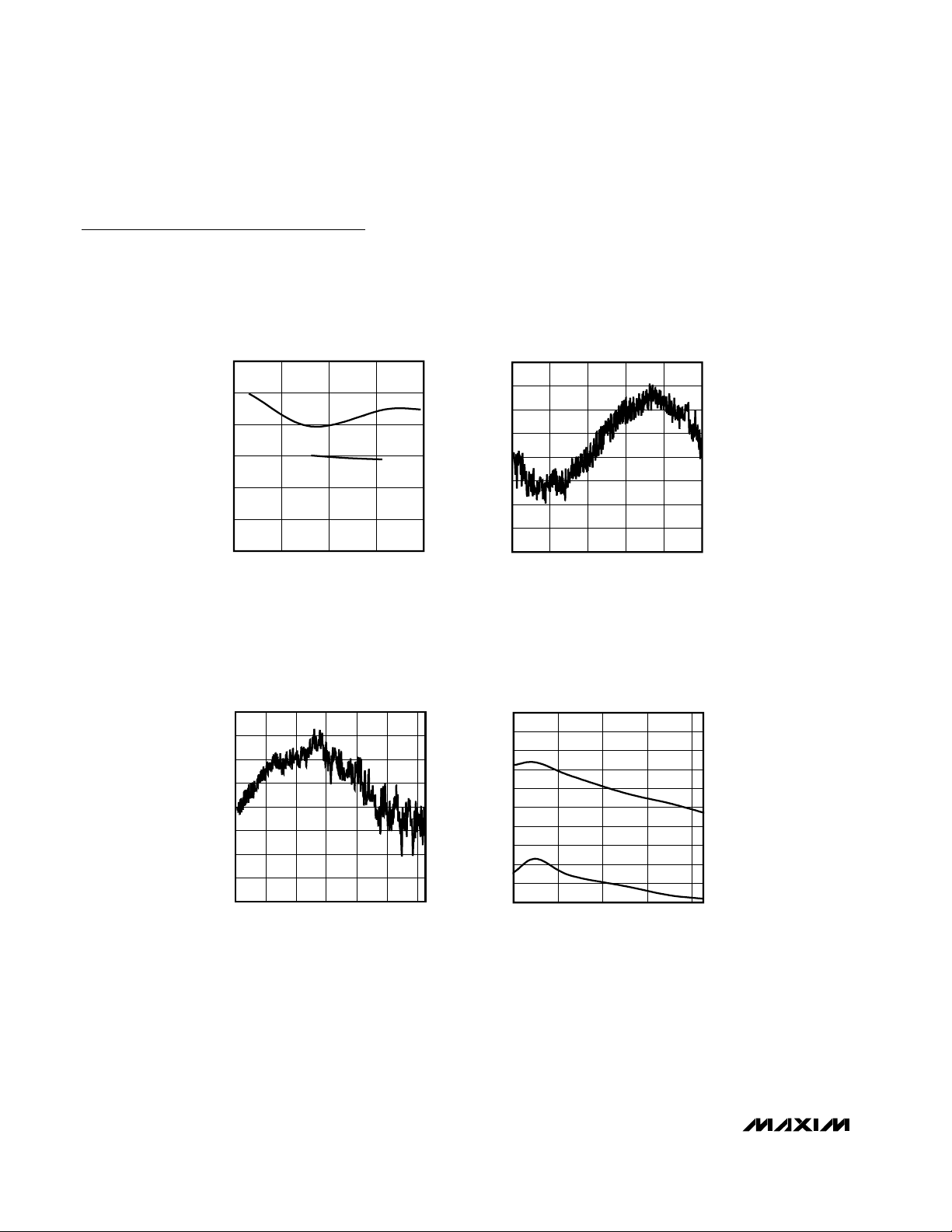
Typical Operating Characteristics (continued)
(A
VDD
= D
VDD
= 3V, MAX1407 used, TA = +25°C, unless otherwise noted.)
0
1
3
2
4
5
2.7 3.12.9 3.3 3.5
MAXIMUM INL vs. V
DD
(UNIPOLAR MODE, T = +25°C,
PSEUDO-DIFFERENTIAL INPUT)
MAX1407 toc05
VDD (V)
MAXIMUM INL (LSB)
A
B
A: GAIN = 1, UNBUFFERED MODE, 60sps
B: GAIN = 1, UNBUFFERED MODE, 30sps
0
1.5
1.0
0.5
2.0
2.5
3.0
3.5
4.0
4.5
5.0
2.7 3.12.9 3.3 3.5
MAXIMUM INL vs. V
DD
(BIPOLAR MODE, T = +25°C,
FULLY DIFFERENTIAL INPUT)
MAX1407 toc06
VDD (V)
MAXIMUM INL (LSB)
A
B
A: GAIN = 2, BUFFERED MODE, 60sps
B: GAIN = 2, BUFFERED MODE, 30sps
0
1.5
1.0
0.5
2.0
2.5
3.0
3.5
4.0
4.5
5.0
04020 60 80
MAXIMUM INL vs. TEMPERATURE
(UNIPOLAR MODE, V
DD
= 3V,
PSEUDO-DIFFERENTIAL INPUT)
MAX1407 toc07
TEMPERATURE (°C)
MAXIMUM INL (LSB)
A
B
A: GAIN = 1, UNBUFFERED MODE, 60sps
B: GAIN = 1, UNBUFFERED MODE, 30sps
0
1.5
1.0
0.5
2.0
2.5
3.0
3.5
4.0
4.5
5.0
04020 60 80
MAXIMUM INL vs. TEMPERATURE
(BIPOLAR MODE, V
DD
= 3V,
FULLY DIFFERENTIAL INPUT)
MAX1407 toc08
TEMPERATURE (°C)
MAXIMUM INL (LSB)
A
B
A: GAIN = 2, BUFFERED MODE, 60sps
B: GAIN = 2, BUFFERED MODE, 30sps
MAX1407/MAX1408/MAX1409/MAX1414
Low-Power, 16-Bit Multichannel DAS with
Internal Reference,10-Bit DACs, and RTC
10 ______________________________________________________________________________________
Typical Operating Characteristics (continued)
(A
VDD
= D
VDD
= 3V, MAX1407 used, TA = +25°C, unless otherwise noted.)
0
1.0
0.5
2.0
1.5
2.5
3.0
0.3 0.70.5 0.9 1.1
MAXIMUM INL vs. COMMON-MODE
INPUT VOLTAGE (BIPOLAR MODE,
BUFFERED MODE, V
DD
= 2.7V, 30sps,
FULLY DIFFERENTIAL INPUT, T = +25°C)
MAX1407 toc09
COMMON-MODE INPUT VOLTAGE (V)
MAXIMUM INL (LSB)
A: GAIN = 1
B: GAIN = 2
A
B
-2.0
-1.5
-1.0
-0.5
0
0.5
1.0
1.5
2.0
-1.25 -0.75 -0.25 0.25 0.75 1.25
INL vs. FULLY DIFFERENTIAL
INPUT VOLTAGE (BIPOLAR MODE,
GAIN = 1, UNBUFFERED MODE,
V
CM
= 0.625V, VDD = 3V, T = +25°C)
MAX1407 toc10
DIFFERENTIAL INPUT VOLTAGE (V)
INL (LSB)
-2.0
-1.5
-1.0
-0.5
0
0.5
1.0
1.5
2.0
0 0.2 0.4 0.8 1.0
INL vs. PSEUDO-DIFFERENTIAL INPUT
VOLTAGE RANGE (UNIPOLAR MODE,
GAIN = 1, UNBUFFERED MODE,
V
NEG
= 0, VDD = 3V, T = +25°C)
MAX1407 toc11
DIFFERENTIAL VOLTAGE (V)
INL (LSB)
1.20.6
0
1.5
1.0
0.5
2.0
2.5
3.0
3.5
4.0
4.5
5.0
04020 60 80
UNCORRECTED OFFSET ERROR
vs. TEMPERATURE
(UNBUFFERED MODE, V
DD
= 3V)
MAX1407 toc12
TEMPERATURE (°C)
OFFSET ERROR (LSB)
A
B
A: GAIN = 1, UNIPOLAR MODE
B: GAIN = 2, BIPOLAR MODE
MAX1407/MAX1408/MAX1409/MAX1414
Low-Power, 16-Bit Multichannel DAS with
Internal Reference,10-Bit DACs, and RTC
______________________________________________________________________________________ 11
REFERENCE
VOLTAGE
(V)
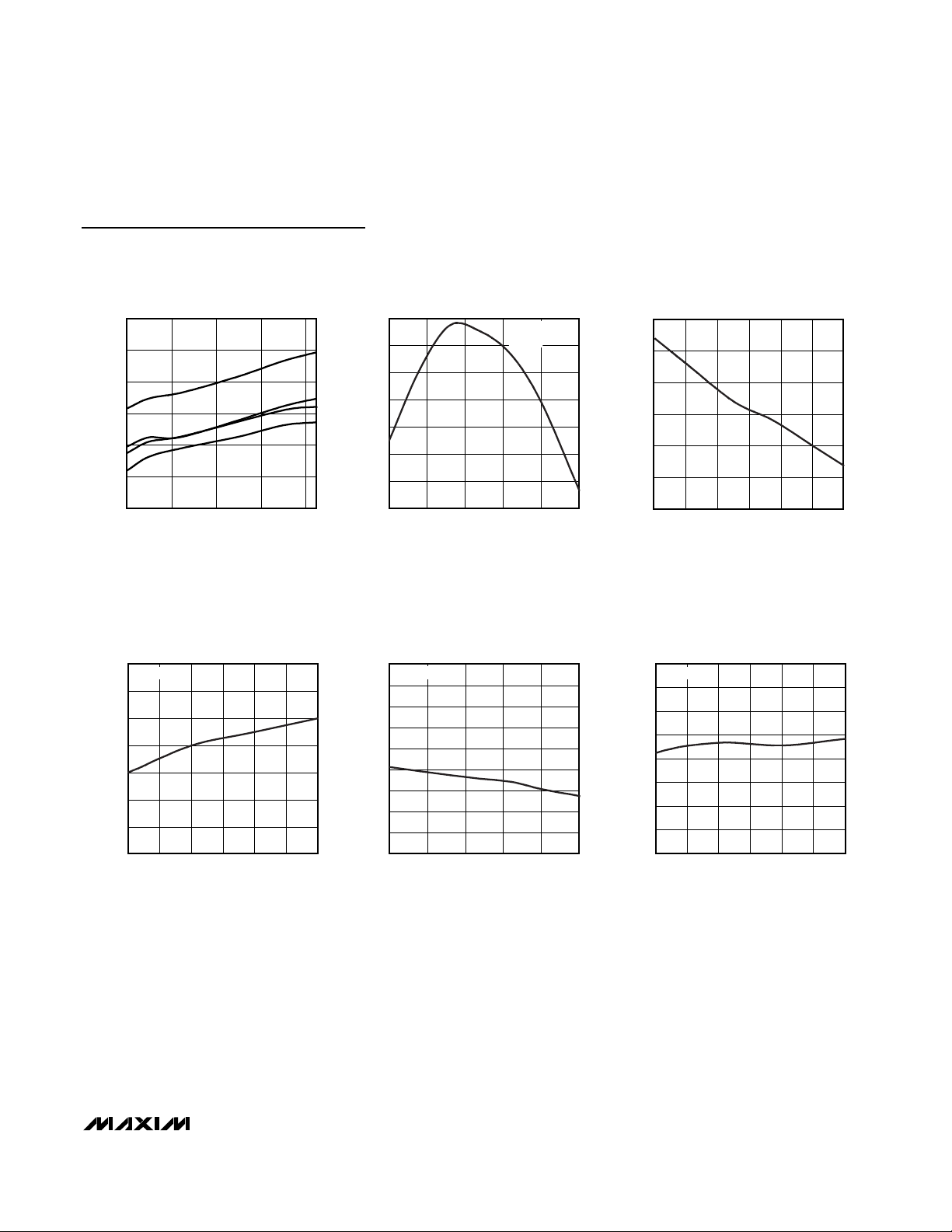
Typical Operating Characteristics (continued)
(A
VDD
= D
VDD
= 3V, MAX1407 used, TA = +25°C, unless otherwise noted.)
GAIN ERROR vs. TEMPERATURE
0.12
VDD = 3V
0.11
0.10
0.09
GAIN ERROR (%)
0.08
C
0.07
0.06
0
A: GAIN = 1, UNIPOLAR MODE, UNBUFFERED MODE
B: GAIN = 1, BIPOLAR MODE, UNBUFFERED MODE
C: GAIN = 2, UNIPOLAR MODE, BUFFERED MODE
D: GAIN = 2, BIPOLAR MODE, BUFFERED MODE
4020 60 80
TEMPERATURE (°C)
REFERENCE VOLTAGE vs.
SUPPLY VOLTAGE
1.24412
NO LOAD
1.24410
1.24408
1.24406
1.24404
1.24402
REFERENCE VOLTAGE (V)
1.24400
1.24398
2.70 3.00 3.152.85 3.30 3.45 3.60
SUPPLY VOLTAGE (V)
REFERENCE VOLTAGE vs.
TEMPERATURE
0.02
B
MAX1407 toc13
D
A
0
-0.02
-0.04
-0.06
% DEVIATION
-0.08
-0.10
-0.12
-40 10-15 35 60 85
TEMPERATURE (°C)
V
REF
= 0
I
REF
= 1.24406V
MAX1407 toc14
1.24410
1.24405
1.24400
1.24395
1.24390
1.24385
1.24380
DAC OFFSET ERROR vs.
TEMPERATURE
MAX1407 toc16
OFFSET ERROR (mV)
-3.4
IDLE MODE
-3.6
-3.8
-4.0
-4.2
-4.4
-4.6
-4.8
-5.0
-5.2
-40 10-15 35 60 85
TEMPERATURE (°C)
-4.400
-4.425
MAX1407 toc17
-4.450
-4.475
-4.500
-4.525
OFFSET ERROR (mV)
-4.550
-4.575
-4.600
REFERENCE VOLTAGE vs.
OUTPUT SOURCE CURRENT
MAX1407 toc15
0 400 600200 800 1000 1200
SOURCE CURRENT (µA)
DAC OFFSET ERROR vs.
SUPPLY VOLTAGE
IDLE MODE
MAX1407 toc18
2.70 3.002.85 3.15 3.30 3.45 3.60
SUPPLY VOLTAGE (V)
MAX1407/MAX1408/MAX1409/MAX1414
Low-Power, 16-Bit Multichannel DAS with
Internal Reference,10-Bit DACs, and RTC
12 ______________________________________________________________________________________
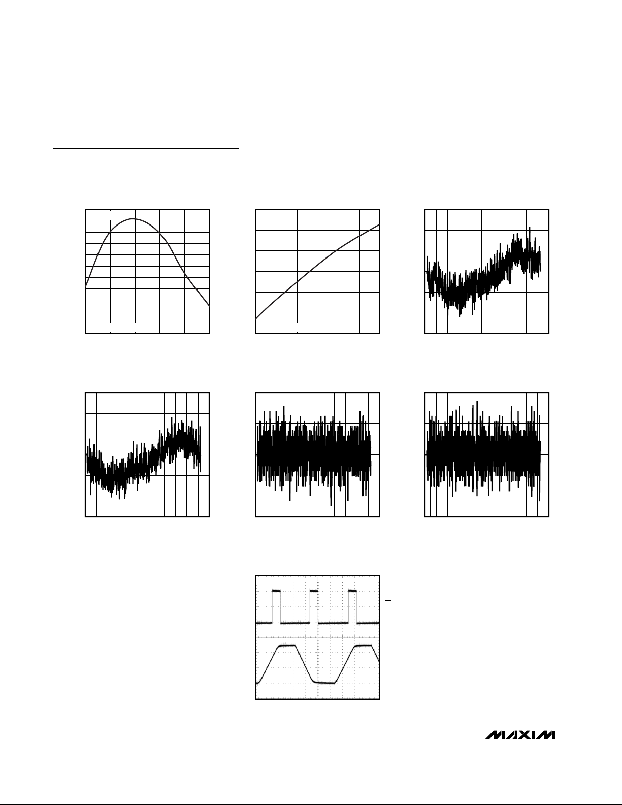
Typical Operating Characteristics (continued)
(A
VDD
= D
VDD
= 3V, MAX1407 used, TA = +25°C, unless otherwise noted.)
-1.50
-1.20
-1.35
-0.60
-0.75
-1.05
0
-0.30
-0.45
0.15
-40 10-15 35 60 85
DAC GAIN ERROR vs.
TEMPERATURE
MAX1407 toc19
TEMPERATURE (°C)
GAIN ERROR (LSB)
-0.15
-0.90
IDLE MODE
INTERNAL REF USED
-0.20
-0.10
-0.15
0
-0.05
0.05
0.10
2.70 3.00 3.152.85 3.30 3.45 3.60
DAC GAIN ERROR vs.
SUPPLY VOLTAGE
MAX1407 toc20
SUPPLY VOLTAGE (V)
GAIN ERROR (LSB)
IDLE MODE
INTERNAL REF USED
-0.15
-0.05
-0.10
0.05
0
0.10
0.15
0 200 300 400100 500 600 700 800 9001000 1100
DAC INTEGRAL NONLINEARITY
vs. DIGITAL CODE (AV
DD
= 2.7V)
MAX1407 toc21
CODE
INL (LSB)
-0.15
-0.05
-0.10
0.05
0
0.10
0.15
0 200 300 400100 500 600 700 800 9001000 1100
DAC INTEGRAL NONLINEARITY
vs. DIGITAL CODE (AV
DD
= 3.6V)
MAX1407 toc22
CODE
INL (LSB)
-0.100
-0.075
0.075
-0.025
-0.050
0
0.025
0.050
0.100
0 200 300 400100 500 600 900800 1000700 1100
DAC DIFFERENTIAL NONLINEARITY
vs. DIGITAL CODE (AV
DD
= 2.7V)
MAX1407 toc23
CODE
DNL (LSB)
-0.100
-0.075
0.075
-0.025
-0.050
0
0.025
0.050
0.100
0 200 300 400100 500 600 900800 1000700 1100
DAC DIFFERENTIAL NONLINEARITY
vs. DIGITAL CODE (AV
DD
= 3.6V)
MAX1407 toc24
CODE
DNL (LSB)
DAC LARGE-SIGNAL OUTPUT
STEP RESPONSE
V
REF
= 1.25V, AVDD = 3.0V, RL = 0
MAX1407 toc25
OUT_
500mV/DIV
CS
2V/DIV
MAX1407/MAX1408/MAX1409/MAX1414
Low-Power, 16-Bit Multichannel DAS with
Internal Reference,10-Bit DACs, and RTC
______________________________________________________________________________________ 13
Typical Operating Characteristics (continued)
(A
VDD
= D
VDD
= 3V, MAX1407 used, TA = +25°C, unless otherwise noted.)
1.2450
1.2445
1.2440
1.2435
1.2430
2.7 3.0 3.3 3.6
DAC OUTPUT VOLTAGE
vs. SUPPLY VOLTAGE
MAX1407 toc26
SUPPLY VOLTAGE (V)
DAC OUTPUT VOLTAGE (V)
OUTPUT AT FULL SCALE
NO LOAD
DAC BUFFER IN UNITY GAIN
1.00
1.10
1.05
1.20
1.15
1.25
1.30
0231 456
DAC OUTPUT VOLTAGE
vs. SOURCE CURRENT
MAX1407 toc27
LOAD CURRENT (mA)
DAC OUTPUT VOLTAGE (V)
OUTPUT AT FULL SCALE
DAC BUFFER IN UNITY GAIN
015
10520253530
40
1.20
1.30
1.35
1.25
1.40
1.45
1.50
1.55
1.60
1.65
1.70
1.75
1.80
DAC OUTPUT VOLTAGE
vs. SINK CURRENT
MAX1407 toc28
SINK CURRENT (µA)
DAC OUTPUT VOLTAGE (V)
-0.15
-0.06
-0.09
-0.12
-0.03
0
0.03
0.06
0.09
0.12
0.15
-40 10-15 35 60 85
DAC OUTPUT VOLTAGE vs.
TEMPERATURE
MAX1407 toc29
TEMPERATURE (°C)
DAC OUTPUT VOLTAGE (%)
V
REF
= 1.24406V
I
REF
= 0
-0.25
-0.15
-0.20
-0.05
-0.10
0.05
0
0.10
-40 10-15 35 60 85
VOLTAGE MONITOR THRESHOLD
vs. TEMPERATURE
MAX1407 toc30
TEMPERATURE (°C)
% DEVIATION
V
1.8V_THRESHOLD
= 1.865V
V
2.7V_THRESHOLD
= 2.75V
MAX1407/MAX1408/MAX1409/MAX1414
Low-Power, 16-Bit Multichannel DAS with
Internal Reference,10-Bit DACs, and RTC
14 ______________________________________________________________________________________
Pin Description
MAX1407
MAX1414
1 ——FB2 Force/Sense DAC2 Feedback Input
— 1 — IN7 Analog Input. Analog input to the negative mux only.
—— 1 FB1 Force/Sense DAC1 Feedback Input
22— D0 Digital Output. Three-state general-purpose digital output.
3 ——FB1 Force/Sense DAC1 Feedback Input
— 3 — IN6 Analog Input. Analog input to the negative mux only.
4 — 2 OUT1 Force/Sense DAC1 Output
— 4 — IN4 Analog Input. Analog input to the positive mux only.
5 5 3 IN0 Analog Input. Analog input to both the positive and negative mux.
6 6 4 REF
7 7 5 AGND
886AVDDAnalog Supply Voltage
9 9 7 CPLL
10 10 8 WU1
11 11 9 WU2
MAX1408 MAX1409 PIN FUNCTION
1.25V Reference Buffer Output/External Reference Input. Reference voltage
for the ADC and the DAC. Connect a 4.7µF capacitor to REF between REF
and AGND.
Analog Ground. Reference point for the analog circuitry. AGND connects to
the IC substrate.
PLL Capacitor Connection Pin. Connect an 18nF ceramic capacitor between
CPLL and AV
Active-Low Wake-Up Input. Internally pulled up. The device will wake-up from
Sleep mode to Standby mode when WU1 is asserted.
Active-Low Wake-Up Input. Internally pulled up. The device will wake-up from
Sleep mode to Standby mode when WU2 is asserted.
DD
.
Active-Low RESET Output. It remains low while AV
12 12 10 RESET
13 13 — IN1 Analog Input. Analog input to both the positive and negative mux.
14 14 — IN2 Analog Input. Analog input to both the positive and negative mux.
15 15 — SHDN Programmable Shutdown Output. Goes low in Sleep mode.
16 16 — DRDY
17 17 11 FOUT 2.4576MHz Clock Output. FOUT can be used to drive the input clock of a µP.
18 18 12 CLKOUT
19 19 13 CLKIN 32kHz Crystal Input. Connect a 32kHz crystal between CLKIN and CLKOUT.
and stays low for a timeout period after AV
RESET is an open-drain output.
Active-Low Data Ready Output. A logic low indicates that a new conversion
result is available in the Data register. DRDY returns high upon completion of
a full output word read operation. DRDY also signals the end of an ADC
offset-calibration.
32kHz Crystal Output. Connect a 32kHz crystal between CLKIN and
CLKOUT.
rises above the threshold.
DD
is below the threshold
DD
MAX1407/MAX1408/MAX1409/MAX1414
Low-Power, 16-Bit Multichannel DAS with
Internal Reference,10-Bit DACs, and RTC
______________________________________________________________________________________ 15
Detailed Information
The MAX1407/MAX1408/MAX1409/MAX1414 are lowpower, general-purpose, multichannel DAS featuring a
multiplexed fully differential 16-bit ∑∆ analog-to-digital
converter (ADC), 10-bit force/sense digital-to-analog
converters (DAC), a real-time clock (RTC) with an
alarm, a bandgap voltage reference, a signal detect
comparator, two power-supply voltage monitors, wakeup control circuitry, and a high-frequency phase-locked
loop (PLL) clock output all controlled by a 3-wire serial
interface. (See Table 1 for the MAX1407/MAX1408/
MAX1409/MAX1414 feature sets and Figures 1, 2, 3 for
the Functional Diagrams). These DAS directly interface
to various sensor outputs and once configured provide
the stimulus, conditioning, and data conversion, as well
as microprocessor support. Figure 4 is a Typical
Application Circuit for the MAX1407/MAX1414.
The 16-bit ∑∆ ADC is capable of programmable continuous conversion rates of 30Hz or 60Hz and gains of
1/3, 1, and 2V/V to suit applications with different power
and dynamic range constraints. The force/sense DACs
provide 10-bit linearity for precise sensor applications.
Pin Description (continued)
Table 1. MAX1407/MAX1408/MAX1409/MAX1414 Feature Sets
MAX1407
MAX1414
20 20 14 INT
21 21 15 DOUT
22 22 16 DIN
23 23 17 SCLK
24 24 18 CS
25 25 19 DGND Digital Ground. Reference point for digital circuitry.
26 26 20 DV
27 27 — IN3 Analog Input. Analog input to both the positive and negative mux.
28 ——OUT2 Force/Sense DAC2 Output
— 28 — IN5 Analog Input. Analog input to the positive mux only.
MAX1408 MAX1409 PIN FUNCTION
Active-Low Interrupt Output. INT goes low when the PLL output is ready,
when the signal-detect comparator is tripped, or when the alarm is triggered.
Serial Data Output. DOUT outputs serial data from the internal shift register
on SCLK’s falling edge. When CS is high, DOUT is three-stated.
Serial Data Input. Data on DIN is written to the input shift register and is
clocked in at SCLK’s rising edge when CS is low.
Serial Clock Input. Apply an external serial clock to transfer data to and from
the device. This serial clock can be continuous, with data transmitted in a
train of pulses, or intermittent while CS is low.
Active-Low Chip-Select Input. CS is used to select the active device in
systems with more than one device on the serial bus. Data will not be
clocked into DIN unless CS is low. When CS is high, DOUT is three-stated.
DD
Digital Supply Voltage
ADC
PART
MAX1407 4 2 Yes 0 Yes Yes Yes 8
MAX1414 4 2 Yes 50 Yes Yes Yes 8
MAX1408 8 0 Yes 0 Yes Yes Yes 8
MAX1409 1 1 No 0 Yes No No 4
AUXILIARY
ANALOG
INPUTS
FORCE/
SENSE
DAC
THREE-
STATE
DIGITAL
OUTPUT
COMPARATOR
THRESHOLD
(mV)
EXTERNAL
RTC
ADC DATA
READY
(DRDY)
POWERSUPPLY
SHUTDOWN
CONTROL
DIFFERENTIAL
INPUT MUX
ADC

MAX1407/MAX1408/MAX1409/MAX1414
Low-Power, 16-Bit Multichannel DAS with
Internal Reference,10-Bit DACs, and RTC
16 ______________________________________________________________________________________
With the use of two external resistors, the DAC output
can go from 0.05V to AVDD- 0.2V. The ADCs and
DACs both utilize a precise low-drift 1.25V internal
bandgap reference for conversions and setting of the
full-scale range. For applications that require increased
accuracy, power-down the internal reference and connect an external reference at REF. The RTC is leap year
compensated until 9999 and provides an alarm function
that can be used to wake-up the system or cause an
interrupt at a predefined time. The power-supply voltage monitors detect when AV
DD
falls below a trip
threshold voltage at either +1.8V or +2.7V causing the
reset to be asserted. The 4-wire serial interface is used
to communicate directly between SPI, QSPI, and
MICROWIRE devices for system configuration and
readback functions.
Analog Input Protection
Internal protection diodes clamp the analog input to
AVDDand AGND, which allow the channel input pins to
swing from AGND - 0.3V to AVDD+ 0.3V without damage. However, for accurate conversions near full scale,
the inputs must not exceed AVDDby more than 50mV
or be lower than AGND by 50mV.
Analog Mux
The MAX1407/MAX1408/MAX1414 include a dual 8 to 1
multiplexer for the positive and negative inputs of the
ADC. The MAX1409 has a dual 4 to 1 multiplexer at the
inputs of the ADC. Figures 1, 2, and 3 illustrate which
signals are present at the inputs of each multiplexer for
the MAX1407/MAX1408/MAX1409/MAX1414. The
MUXP and MUXN bits of the MUX register choose
which inputs will be seen at the input to the ADC
(Tables 4 and 5) and the signal-detect comparator. See
the MUX Register description under the On-Chip
Registers section for multiplexer functionality.
Input Buffers
The MAX1407/MAX1408/MAX1409/MAX1414 provide
input buffers to isolate the analog inputs from the capacitive load presented by the ADC modulator (Figure 5 and
6). The buffers are chopper stabilized to reduce the effect
of their DC offsets and low-frequency noise. Since the
buffers can represent more than 25% of the total analog
power dissipation (typically 220µA), they may be shut
down in applications where minimum power dissipation is
required and the capacitive input load is not a concern
(see ADC and Power1 Registers). Disable the buffers in
applications where the inputs must operate close to
AGND or above +1.4V. The buffers are individually
enabled or disabled.
Figure 1. MAX1407/MAX1414 Functional Diagram
CPLL FOUT CLKIN CLKOUT
AV
DD
DV
DD
CS
SCLK
DIN
DOUT
IN3
IN2
IN1
IN0
*MAX1414 HAS A +50mV SIGNAL-DETECT COMPARATOR THRESHOLD.
OUT2
OUT1
REF
AV
FB2
FB1
REF
AGND
IN3
IN2
IN1
IN0
DD
SERIAL
INTERFACE
8:1
INPUT
MUX
8:1
INPUT
MUX
AGND
2.4576MHz
PLL
1.8V/2.7V
SUPERVISORS
GENERATOR
RESET
RESET
BUF
BUF
µP
32.768kHz
OSCILLATOR
COMPARATOR
1.25V
BANDGAP
REFERENCE
RTC AND
ALARM
MAX1407/MAX1414
16-BIT ADC
PGA
BUF
REF
10-BIT DAC
10-BIT DAC
WAKE-UP
LOGIC
INTERRUPT
GENERATOR
DIGITAL
OUTPUT
DGND
WU2
WU1
SHDN
INT
DRDY
D0
OUT1
FB1
OUT2
FB2

MAX1407/MAX1408/MAX1409/MAX1414
Low-Power, 16-Bit Multichannel DAS with
Internal Reference,10-Bit DACs, and RTC
______________________________________________________________________________________ 17
Figure 3. MAX1409 Functional Diagram
Figure 2. MAX1408 Functional Diagram
CS
SCLK
DIN
DOUT
IN5
IN4
IN3
IN2
IN1
IN0
REF
AV
DD
IN7
IN6
REF
AGND
IN3
IN2
IN1
IN0
AV
DD
SERIAL
INTERFACE
8:1
INPUT
MUX
8:1
INPUT
MUX
AGND
CPLL FOUT CLKIN CLKOUT
BUF
BUF
µP
RESET
RESET
32.768kHz
OSCILLATOR
COMPARATOR
1.25V
BANDGAP
REFERENCE
PGA
BUF
REF
2.4576MHz
PLL
1.8V/2.7V
SUPERVISORS
GENERATOR
RTC AND
ALARM
16-BIT ADC
INTERRUPT
GENERATOR
MAX1408
DV
DD
WAKE-UP
LOGIC
DIGITAL
OUTPUT
DGND
WU2
WU1
SHDN
INT
DRDY
D0
CS
SCLK
DIN
DOUT
OUT1
IN0
REF
AV
DD
FB1
IN0
REF
AGND
AV
DD
SERIAL
INTERFACE
4:1
INPUT
MUX
4:1
INPUT
MUX
AGND
CPLL FOUT CLKIN CLKOUT
BUF
BUF
µP
32.768kHz
OSCILLATOR
COMPARATOR
1.25V
BANDGAP
REFERENCE
PGA
BUF
REF
2.4576MHz
PLL
1.8V/2.7V
SUPERVISORS
GENERATOR
RESET
RESET
RTC AND
ALARM
16-BIT ADC
10-BIT DAC
GENERATOR
MAX1409
DV
DD
WAKE-UP
LOGIC
INTERRUPT
DGND
WU2
WU1
INT
OUT1
FB1

MAX1407/MAX1408/MAX1409/MAX1414
Low-Power, 16-Bit Multichannel DAS with
Internal Reference,10-Bit DACs, and RTC
18 ______________________________________________________________________________________
Buffered Mode
When used in buffered mode, the buffers isolate the
inputs from the sampling capacitors. The samplingrelated gain error is dramatically reduced since only a
small dynamic load is present from the chopper. The
multiplexer exhibits an input leakage current of 0.5nA
(typ). With high-source resistances, this leakage current may result in a large DC offset error.
Figure 4. MAX1407/MAX1414 Typical Application Circuit
Figure 5. Analog Input—Buffered Mode
= 3.3V OR V
V
LX
LX
MAX1833
OUT
RST
DD
10µF
18nF
BAT
0.1µF 0.1µF
0.1µF
10µF
SENSOR
GND
4.7µF
SHDN
CPLL
SHDN
IN0
REF
R
L
IN1
R
T
OUT1
R
F
FB1
WE
RE
CE
FB2
OUT2
BATT
V
BAT
AV
DD
MAX1407
MAX1414
AGND DGND
DV
DD
RESET
CLKIN
CLKOUT
FOUT
CS
SCLK
DIN
DOUT
INT
DRDY
WU1 I/O
WU2 I/O
32.768kHz
RESET
CLKIN
OUTPUT
SCK
MOSI
MISO
INPUT
INPUT
V
DD
µP/µC
V
SS
R
EXT
C
EXT
R
MUX
C
PIN
R
IN
C
ST
C
AMP
C
SAMPLE
C
C
MAX1407/MAX1408/MAX1409/MAX1414
Low-Power, 16-Bit Multichannel DAS with
Internal Reference,10-Bit DACs, and RTC
______________________________________________________________________________________ 19
Unbuffered Mode
When used in unbuffered mode, the switched capacitor
sampling front end of the modulator presents a dynamic load to the driving circuitry. The size of the internal
sampling capacitor and the input sampling frequency
(Figure 6) determines the dynamic load (see Dynamic
Input Impedance section). As the gain increases, the
input sampling capacitance also increases. Since the
MAX1407/MAX1408/MAX1409/MAX1414 sample at a
constant rate for all gain settings, the dynamic load presented by the inputs varies with the gain setting.
PGA Gain
An integrated programmable-gain amplifier (PGA) provides three user-selectable gains: +1/3V/V, +1V/V, and
+2V/V to maximize the dynamic range of the ADC. Bits
GAIN1 and GAIN0 set the desired gain (see ADC
Register). The gain of +1/3V/V allows the direct measurement of the supply voltage through an internal multiplexer input or through an auxillary input.
ADC Modulator
The MAX1407/MAX1408/MAX1409/MAX1414 perform
analog-to-digital conversions using a single-bit, second-order, switched-capacitor delta-sigma modulator.
The delta-sigma modulation converts the input signal
into a digital pulse train whose average duty cycle represents the digitized signal information. The pulse train
is then processed by a digital decimation filter.
The modulator provides 2nd-order frequency shaping
of the quantization noise resulting from the single bit
quantizer. The modulator is fully differential for maximum signal-to-noise ratio and minimum susceptibility to
power-supply noise. The modulator operates at one of
two different sampling rates resulting in an output data
rate of either 30Hz or 60Hz (see ADC Register).
ADC Offset Calibration
The MAX1407/MAX1408/MAX1409/MAX1414 are capable of performing digital offset correction to eliminate
changes due to power-supply voltage or system temperature. At the end of a calibration cycle, a 16-bit calibration value is stored in the Offset register in two’s
compliment format. After completing a conversion, the
MAX1407/MAX1408/MAX1409/MAX1414 subtract the
calibration value from the ADC conversion result and
write the offset compensated data to the Data register
(see Offset Register section). Either a positive or nega-
tive offset can be calibrated. During offset calibration,
DRDY will go high. DRDY goes low after calibration is
complete. The offset register can be programmed to
skew the ADC offset with a maximum range from -215to
(+215- 1)LSBs, e.g., if the programmed 2’s complement
value is +2LSB (-2LSB), this translates to a -2LSB
(+2LSB) shift in bipolar mode or a -4LSB (+4LSB) shift in
unipolar mode.To maintain optimum performance, recalibrate the ADC if the temperature changes by more than
20°C. Offset calibration should also be performed after
any changes in PGA gain, bipolar/unipolar input range,
buffered/unbuffered mode, or conversion speed. During
calibration, the two mulitplexers will be disabled and the
inputs to the ADC will internally be shorted to a common-mode voltage.
ADC Digital Filter
The on-chip digital filter processes the 1-bit data
stream from the modulator using a SINC3filter function.
The SINC3filters settle in three data word periods. The
settling time is 3/60Hz or 50ms (for RATE bit in ADC
register set to 1) and 3/30Hz or 100ms (for RATE bit set
to “0”).
ADC Digital Filter Characteristics
The transfer function for a SINC3filter function is that of
three cascaded SINC1filters. This can be described in
the Z-domain by:
and in the frequency domain by:
where N, the decimation factor, is the ratio of the modulator frequency f
M
to the output frequency fN.
Figure 6. Analog Input—Unbuffered Mode
R
EXT
C
EXT
R
MUX
C
PIN
R
SW
CSTC
SAMPLE
C
C
H ƒ
Hz
()
=
()
1
−
()
1
=
N
1
()
sin
1
N
sinππ
3
−
N
z
1
−
−
z
3
ƒ
N
ƒ
M
ƒ
ƒ
M
MAX1407/MAX1408/MAX1409/MAX1414
Low-Power, 16-Bit Multichannel DAS with
Internal Reference,10-Bit DACs, and RTC
20 ______________________________________________________________________________________
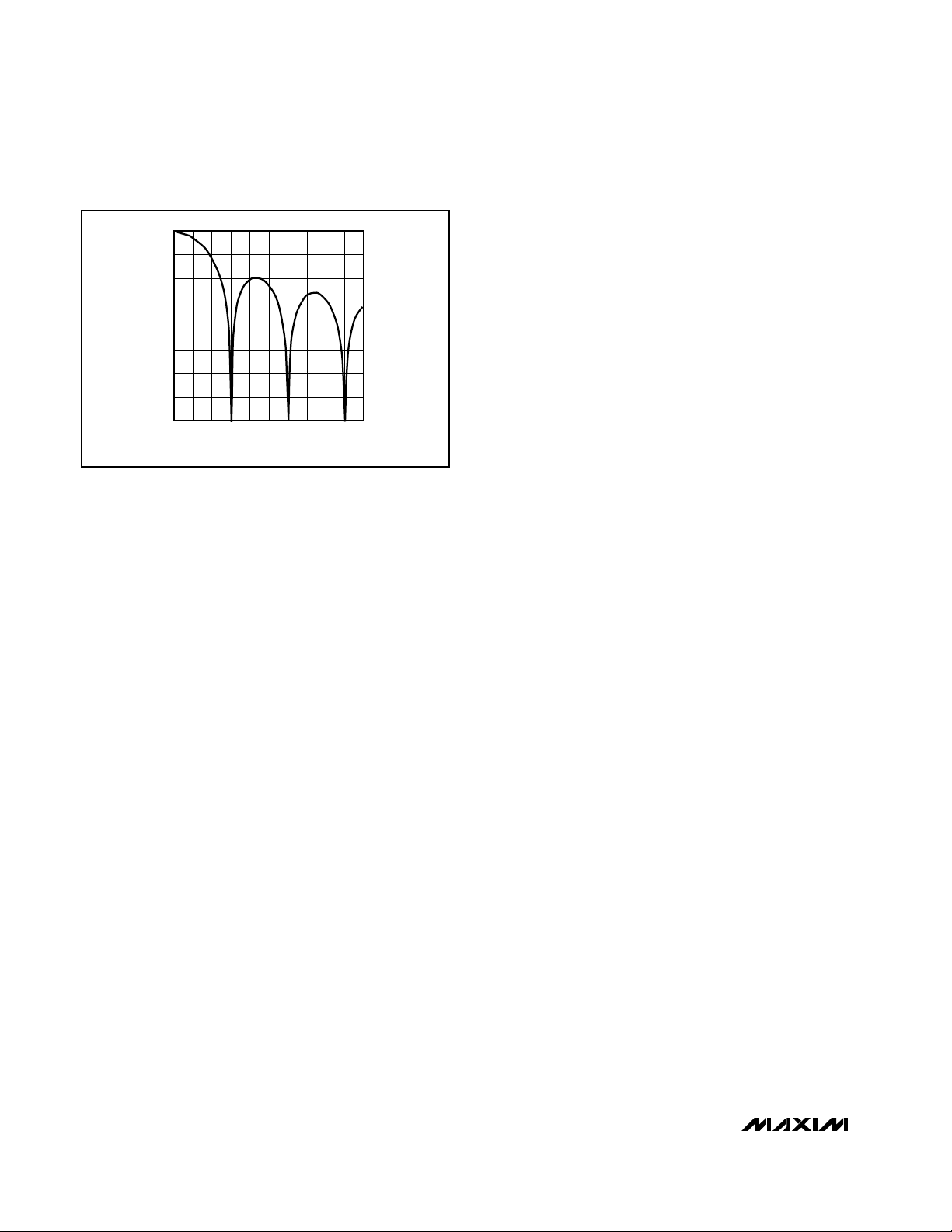
Figure 7 shows the filter frequency response. The
SINC3characteristic cutoff frequency is 0.262 times the
first notch frequency. This results in a cutoff frequency
of 15.72Hz for a first filter notch frequency of 60Hz (output data rate of 60Hz). The response shown in Figure 7
is repeated at either side of the digital filter’s sample
frequency (fM) (fM= 15.36kHz for 30Hz and fM=
30.72kHz for 60Hz) and at either side of the related har-
monics (2fM, 3fM,....).
The output data rate for the digital filter corresponds
with the positioning of the first notch of the filter’s frequency response. Therefore, for the plot of Figure 7
where the first notch of the filter is at 60Hz, the output
data rate is 60Hz. The notches of this (sinx/x)3 filter are
repeated at multiples of the first notch frequency. The
SINC3filter provides an attenuation of better than
100dB at these notches.
For step changes at the input, enough settling time
must be allowed before valid data can be read. The
settling time depends upon the output data rate chosen
for the filter. The settling time of the SINC3filter to a fullscale step input can be up to four times the output data
period, or three times if the step change is synchrozied
with FSYNC.
Force/Sense DAC
(MAX1407/MAX1409/MAX1414)
The MAX1407/MAX1414 incorporate two 10-bit force/
sense DACs while the MAX1409 has one. The DACs
use a precise 1.25V internal bandgap reference for setting the full-scale range. Program the DAC1 and DAC2
registers through the serial interface to set the output
voltages of the DACs seen at OUT1 and OUT2.
Shorting FB1(2) and OUT1(2) configures the DAC in a
unity-gain setting. Connecting resistors in a voltagedivider configuration between OUT1(2), FB1(2), and
GND sets a different closed-loop gain for the output
amplifier (see the Applications Information section).
The DAC output amplifier typically settles to ±
1
/
2
LSB
from a full-scale transition within 65µs, when it is connected in unity gain and loaded with 12kΩ in parallel
with 200pF. Loads less than 2kΩ may degrade performance. See the Typical Operating Characteristics section for the source-and-sink capabilty of the DAC
output.
The MAX1407/MAX1409/MAX1414 feature a softwareprogrammable shutdown mode for the DACs that
reduce the total power consumption when they are not
used. The two DACs can be powered-down independently or simultaneously by clearing the DA1E and
DA2E bits (see Power1 Register). DAC outputs OUT1
and OUT2 go high impedance when powered down.
The DACs are automatically powered up and ready for
a conversion when Idle or Run mode is entered.
Voltage Monitors
The MAX1407/MAX1408/MAX1409/MAX1414 include
two on-board voltage monitors. When AVDDis below
the RESET trip threshold, RESET goes low and the RST
bit of the Status register is set to “1”. When AV
DD
is
below the Low VDDtrip threshold, the LVD bit of the
Status register is set to 1.
RESET
Voltage Monitor
The RESET voltage monitor is powered up at all times
(provided that VM = 0 and LVDE = 1 or VM = 1 and
LSDE = 1). A threshold voltage of either +1.8V or +2.7V
may be selected for the RESET voltage monitor (see
Power2 Register). At initial power-up, the RESET trip
threshold is set to 2.7V. If the RESET voltage monitor is
tripped, the RST bit of the status register is set to “1”
and RESET goes low. RESET is held low for 1.54
seconds (typ) after AV
DD
rises above the RESET voltage
monitor threshold. If AVDDis no longer below the RESET
threshold, reading the Status register will clear RST.
Low VDDVoltage Monitor
When the device is operating in Run, Idle, or Standby
mode (see Power Modes) and AVDDgoes below +2.7V,
the low V
DD
monitor trips, indicating that the supply voltage is below the safe minimum for proper operation.
When tripped, the Low V
DD
Voltage Monitor sets the LVD
bit of the Status register to 1. If AV
DD
is no longer below
+2.7V, reading the Status register will clear LVD. The low
VDDmonitor is powered down in Sleep mode. When it is
powered down, the LVD bit stays unchanged. The LVD is
cleared if it is read in Sleep mode.
Figure 7. Frequency Response of the SINC3Filter (Notch at
60Hz)
0
-20
-40
-60
-80
GAIN (dB)
-100
-120
-140
-160
0 40608020 100 120 140 160 180 200
FREQUENCY (Hz)

MAX1407/MAX1408/MAX1409/MAX1414
Low-Power, 16-Bit Multichannel DAS with
Internal Reference,10-Bit DACs, and RTC
______________________________________________________________________________________ 21
Internal/External Reference
The MAX1407/MAX1408/MAX1409/MAX1414 have an
internal low-drift +1.25V reference used for both ADC
and DAC conversion. The buffered reference output
can be used as a reference source for other devices in
the system. The internal reference requires a 4.7µF lowESR ceramic capacitor or tantalum capacitor connected between REF and AGND. For applications that
require increased accuracy, power-down the internal
reference by writing a 0 to the REFE bit of the Power1
register and connect an external reference source to
REF. The valid external reference voltage range is
1.25V ±100mV.
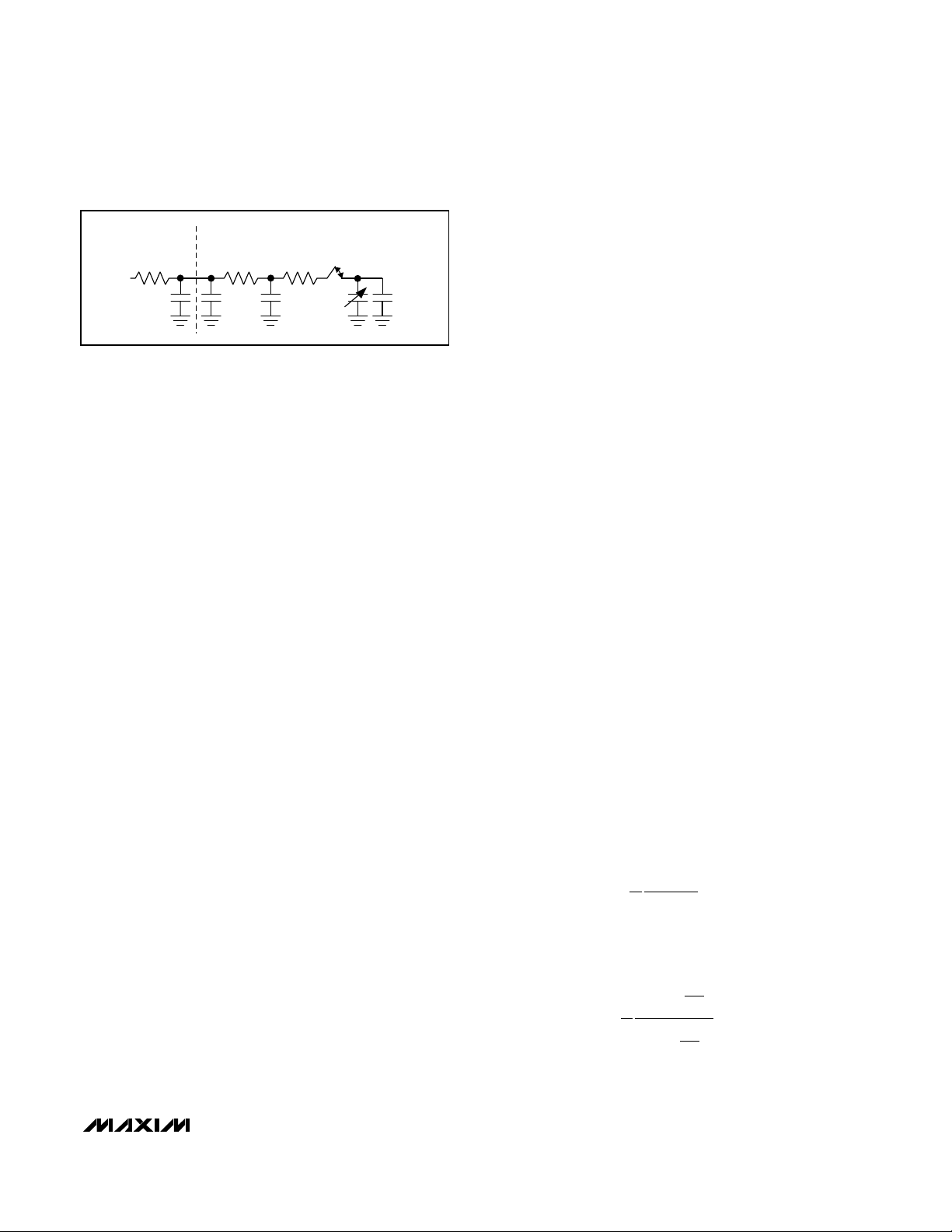
Crystal Oscillator
The on-chip oscillator requires an external crystal (or
resonator) connected between CLKIN and CLKOUT
with an operating frequency of 32.768kHz. This oscillator is used for the RTC, alarm, signal-detect comparator, and PLL. The oscillator is operational down to 1.8V.
In any crystal-based oscillator circuit, the oscillator frequency is based on the characteristics of the crystal. It
is important to select a crystal that meets the design
requirements, especially the capacitive load (CL) that
must be placed across the crystal pins in order for the
crystal to oscillate at its specified frequency. CLis the
capacitance that the crystal needs to “see” from the
oscillator circuit; it is not the capacitance of the crystal
itself. The MAX1407/MAX1408/MAX1409/MAX1414
have 6pF of capacitance across the CLKIN and CLKOUT pins. Choose a crystal with a 32.768kHz oscillation
frequency and a 6pF capacitive load such as the C002RX32-E from Epson Crystal. Using a crystal with a
C
L
that is larger than the load capacitance of the oscillator circuit will cause the oscillator to run faster than
the specified nominal frequency of the crystal.
Conversely, using a crystal with a C
L
that is smaller
than the load capacitance of the oscillator circuit will
cause the oscillator to run slower than the specified
nominal frequency of the crystal.
Phase-Locked Loop (PLL) and FOUT
An on-board phase-locked loop generates a
2.4576MHz clock at FOUT from the 32.768kHz crystal
oscillator. FOUT can be used to clock a µP or other digital circuitry. Connect an 18nF ceramic capacitor from
CPLL to AVDDto create the 2.4576MHz clock signal at
FOUT. To power down the PLL, clear PLLE in the
Power2 register (see Power2 Register) or write to the
Sleep register. FOUT will be active for 1.95ms (t
DFOF
)
after receiving either power-down command and then
go low. This provides extra clock signals to the µP to
complete a shutdown sequence. The PLL is active in all
modes except the sleep mode (see Power Modes). To
reactivate the PLL, the following conditions must be
met: AV
DD
is greater than the low VDDvoltage monitor
threshold, RESET is deasserted, and the PLLE bit is
equal to “1”. FOUT is enabled 31.25ms (t
DFON
) after
the PLL is activated. At initial power-up, the PLL is
enabled. If RESET is asserted while the PLL is running,
the PLL does not shut down.
Real-Time Clock (RTC)
The integrated RTC provides the current second,
minute, hour, date, month, day, year, century, and millenium information. An internally generated reference
clock of 1.024kHz (derived from the 32.768kHz crystal)
drives the RTC. The RTC operates in either 24-hour or
12-hour format with an AM/PM indicator (see RTC_Hour
Register). An internal calendar compensates for months
with less than 31 days and includes leap year correction through the year 9999. The RTC operates from a
supply voltage of +1.8V to +3.6V and consumes less
than 1µA current.
Time of Day Alarm
The MAX1407/MAX1408/MAX1409/MAX1414 offer a time
of day alarm which generates an interrupt when the RTC
reaches a preset combination of seconds, minutes,
hours, and day (see Alarm Registers). In addition to setting a “single-shot” alarm, the Time of Day Alarm can
also be programmed to generate an alarm every second, minute, hour, day, or week. “Don’t care” states can
be inserted into one or more fields if it is desired for them
to be ignored for the alarm condition. The Time of Day
Alarm wakes up the device into Standby mode if it is in
Sleep mode. The Time of Day Alarm operates from a
supply voltage of +1.8V to +3.6V.
Interrupt (
IINNTT
)
INT indicates one of three conditions. After receiving a
valid interrupt (INT goes low), read the Status register
and the Al_Status register (if the alarm is enabled) to
identify the source of the interrupt. The three sources of
interrupts are from the CLK, SDC, and ALIRQ bits.
PLL Ready
On power-up, INT is high. 7.82ms (t
DFI
) after the PLL
output appears on FOUT, INT goes low (see Figure 15).
The CLK bit of the Status register is set to “1” after
FOUT is enabled. Reading the Status register clears the
CLK bit. INT remains low until the device detects a start
bit through the serial interface from the µP. The purpose
of this interrupt is to inform the µP that the FOUT clock
signal is present.
MAX1407/MAX1408/MAX1409/MAX1414
Low-Power, 16-Bit Multichannel DAS with
Internal Reference,10-Bit DACs, and RTC
22 ______________________________________________________________________________________
Signal Detect
The INT pin will also go low and stay low when the differential voltage on the selected analog inputs exceeds
the signal-detect comparator trip threshold (0mV for the
MAX1407/MAX1408/MAX1409 and 50mV for the
MAX1414). This will latch the SDC bit of the Status register to one. Additional signal detect interrupts cannot
be generated unless the SDC bit is cleared. To clear
the SDC bit, the Status register must be read and the
input must be below the signal-detect threshold.
Powering down the signal detect-comparator without
reading the Status register will also clear the SDC bit.
Similar to the power-up case, INT goes high when the
device detects a start bit through the serial interface
from the µP.
Time of Day Alarm
If the device is in Sleep mode, the alarm will wake up
the device and set the ALIRQ bit. INT is asserted when
the PLL is turned on. If an alarm occurs while the
device is awake (BIASE = 1), the ALIRQ bit will be set
and INT will go low. INT remains low until the device
detects a start bit through the serial interface from the
µP. ALIRQ is reset to 0 when any alarm register is read
or written to.
Shutdown (
SSHHDDNN
)
SHDN is an active-low output that can be used to control an external power supply. Powering up the PLL
(PLLE = 1) or writing a “1” to the SHDE bit of the
Power2 register causes SHDN to go high. SHDN goes
low when the SHDE bit is set to 0 only if the PLL is powered down (PLLE = 0). The SHDN output stays high for
2.93ms (t
DPD
) after receiving a power-down command,
allowing the external power supply to stay alive so that
the µP can properly complete a shutdown sequence.
SHDN is not available on the MAX1409. Note: Entering
Sleep mode automatically sets PLLE and SHDE to 0.
Any wake-up event will cause SHDN to go high. (See
Wake-Up section.)
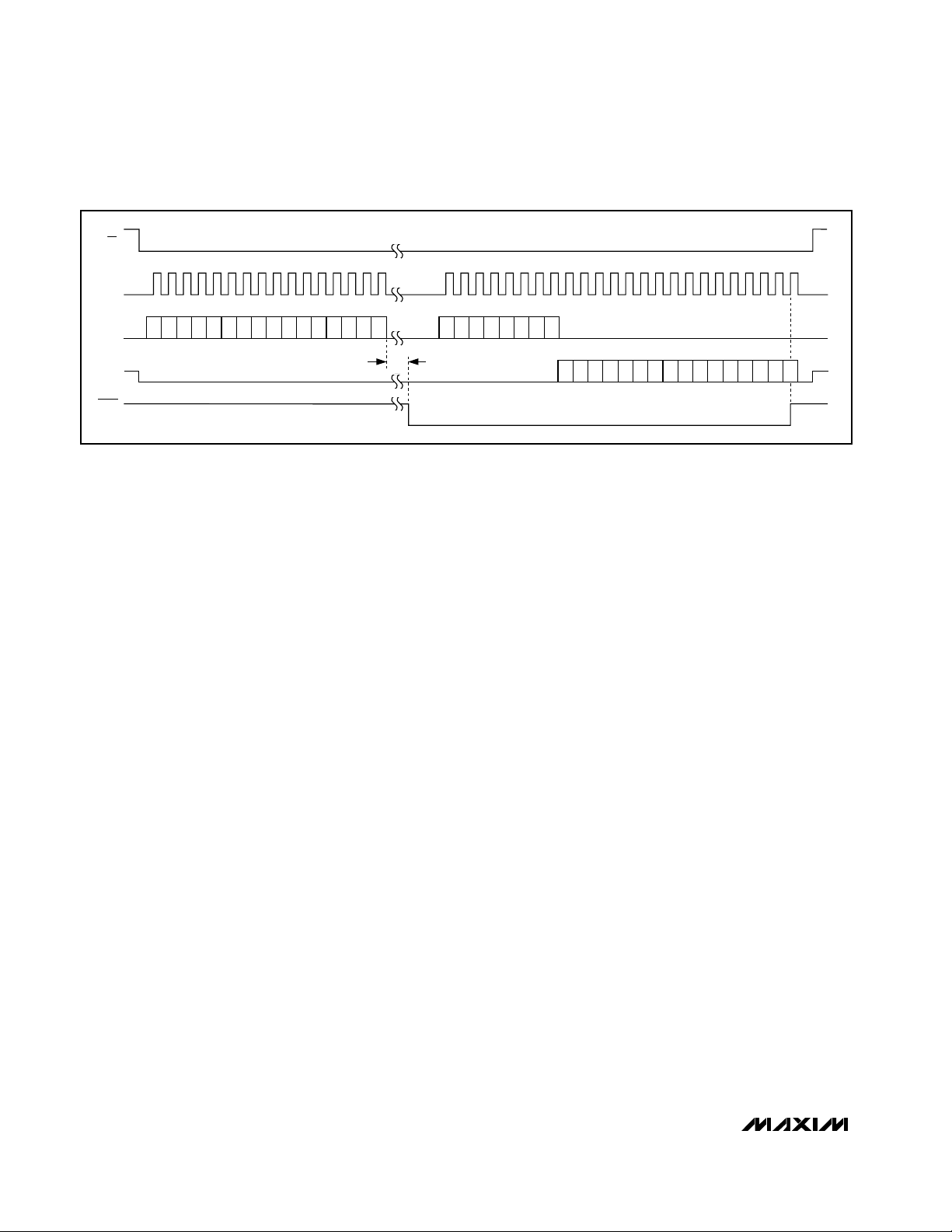
Data Ready (
DDRRDDYY
)
This pin will go low and stay low upon completion of an
ADC conversion or end of an ADC calibration. This signals the µP that a valid conversion or calibration result
has been written to the DATA or the OFFSET register.
The DRDY pin goes high either when the µP has finished reading the conversion/calibration result on the
last rising edge of SCLK (see Figure 8), or when the
next conversion result is about to be written to the
DATA register. When no read operation is performed,
DRDY pulses at 60Hz with a pulse high time of
162.76µs (or 30Hz with a pulse high time of 325.52µs)
DRDY is not available on the MAX1409. To see when
the ADC has completed a normal conversion or a calibration conversion for the MAX1409, check the status
of the ADD bit in the Status register.
Serial Digital Interface
The SPI/QSPI/MICROWIRE-serial interface consists of
chip select (CS), serial clock (SCLK), data in (DIN), and
data out (DOUT) (See Figure 9). The serial interface
provides access to 29 on-chip registers, allowing control to all the power modes and functional blocks,
including the ADCs, DACs, and RTC. Table 2 lists the
address and read/write accessibility of all the registers.
A logic high on CS three-states DOUT and causes the
MAX1407/MAX1408/MAX1409/MAX1414 to ignore any
signals on SCLK and DIN. To clock data into or out of
the internal shift register, drive CS low. SCLK synchronizes the data transfer. The rising edge of SCLK clocks
DIN into the shift register, and the falling edge of SCLK
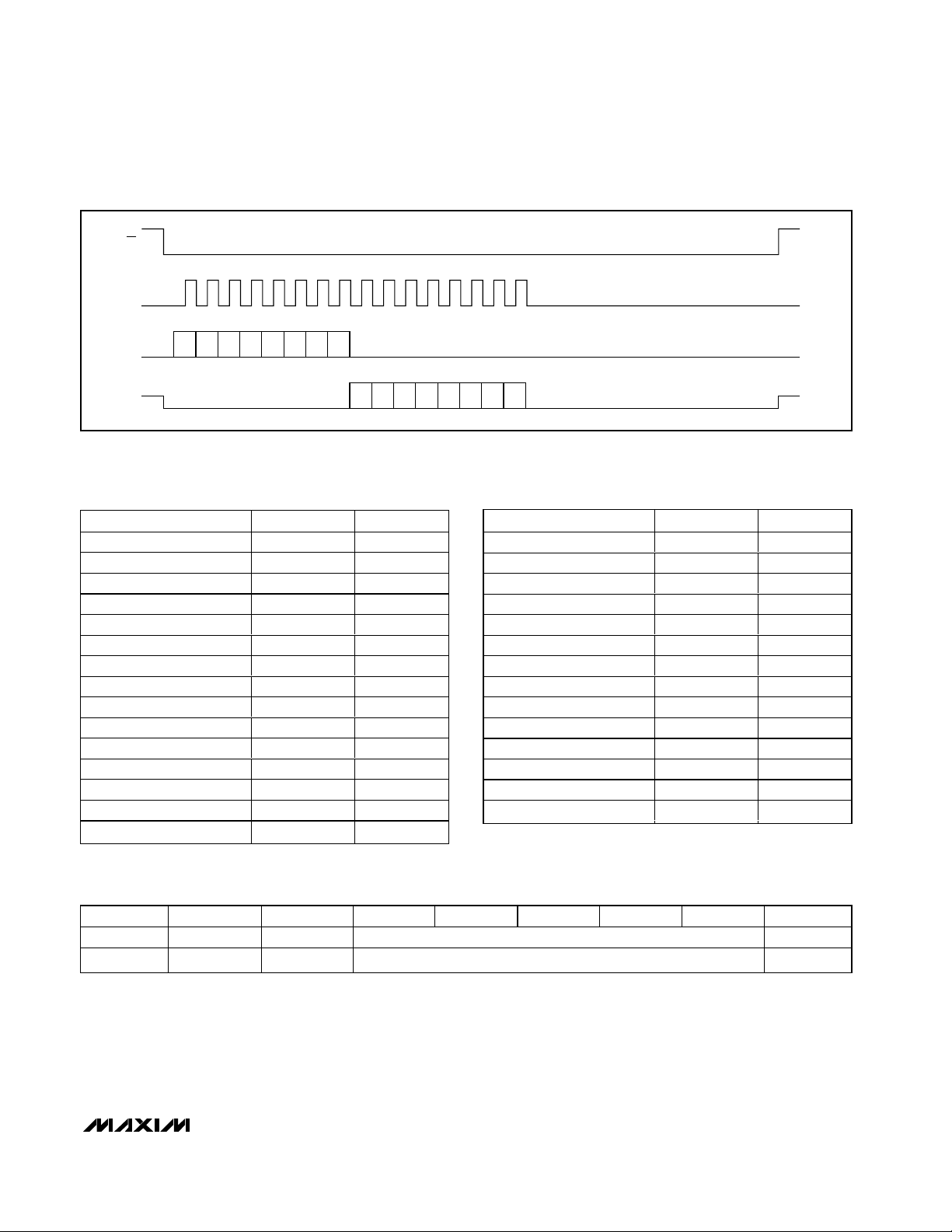
Figure 8. ADC Conversion Timing Diagram
CS
SCLK
DIN
DOUT
DRDY
1 0 A4 A3 A2 A1 A0 x 1 1 A4 A3 A2 A1 A0 x
D7 D6 D5 D4 D3 D2 D1 D0
ADC
CONV
D15 D14 D13 D12 D11 D10
D7 D6 D5 D4 D3 D2 D1 D0D8D9
MAX1407/MAX1408/MAX1409/MAX1414
Low-Power, 16-Bit Multichannel DAS with
Internal Reference,10-Bit DACs, and RTC
______________________________________________________________________________________ 23
clocks DOUT out of the shift register. DIN and DOUT are
transferred as MSB first (data is left justified). Figure 10
shows detailed serial interface timing.
All communication with the MAX1407/MAX1408/
MAX1409/MAX1414 begins with a command byte on
DIN, where the first logic 1 on DIN will be recognized as
the START bit (MSB) for the command byte (Table 3).
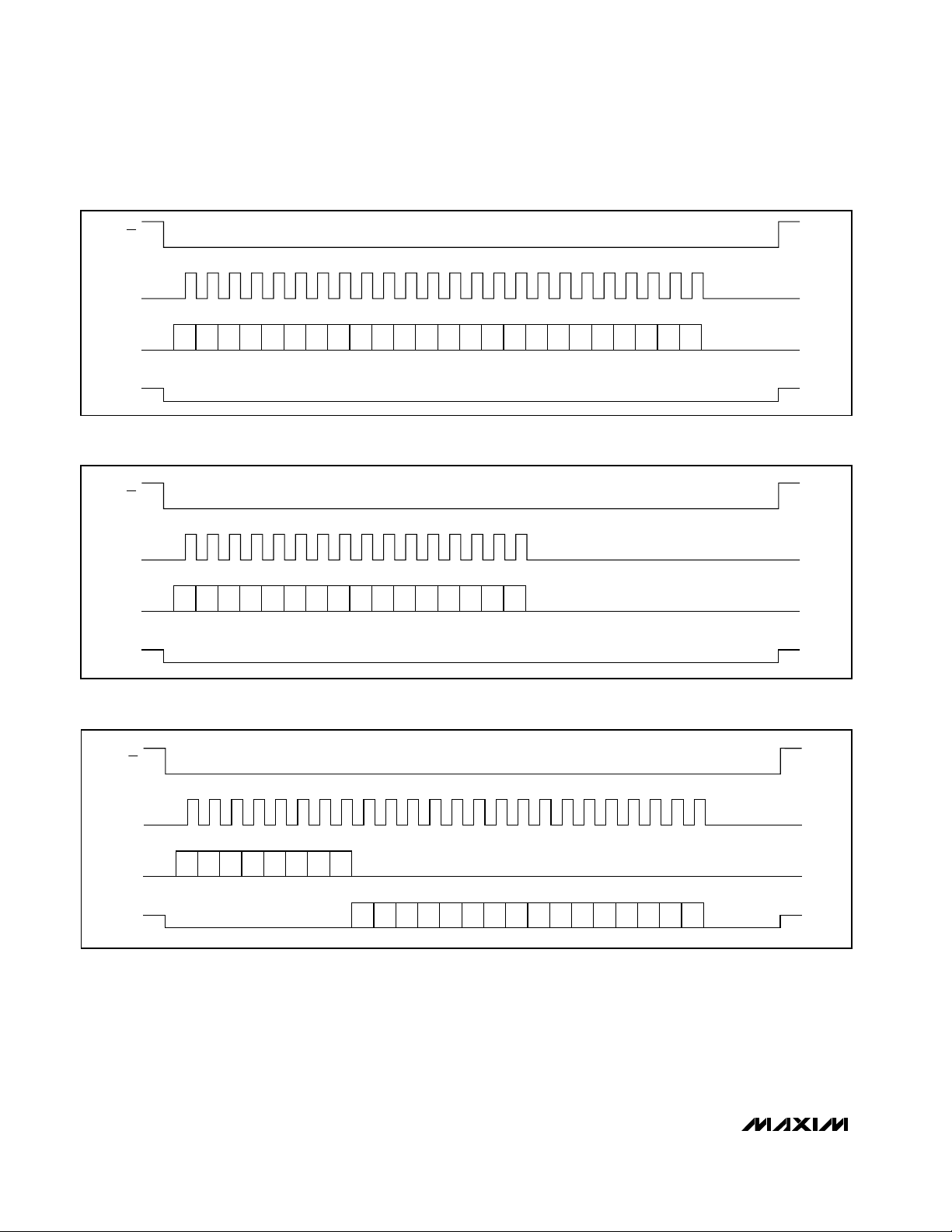
The following seven clock cycles load the command into
a shift register. These seven bits specify which of the
registers will be accessed, whether a read or write operation will take place, and the length of the subsequent
data (0-bit, 8-bit, 16-bit, or burst mode). Idle DIN low
between writes to the MAX1407/MAX1408/MAX1409/
MAX1414. Figures 11–14 show the read and write timing
for 8- and 16-bit data. Data is updated on the last rising
edge of the SCLK in the command word. CS should not
go high between data transfers. If CS is toggled before
the end of a write or read operation, the device can
enter an incorrect mode. Clock in 72 zeros to clear this
state and re-arm the serial interface.
After loading the command byte into the shift register,
additional clocks shift out data on DOUT for a read and
shift in data on DIN for a write operation.
Figure 9. SPI/QSPI Interface Connections
Figure 10. Detailed Serial Interface Timing
CLKOUT
MAX1407
MAX1408
MAX1409
MAX1414
CLKIN
32.768kHz
FOUT
RESET
CS
SCLK
DIN
DOUT
INT
DRDY
WU1 I/O
WU2 I/O
µP/µC
CLKIN
RESET
OUTPUT
SCK
MOSI
MISO
INPUT
INPUT
CS
t
CSS
t
DS
t
DH
t
DV
SCLK
DIN
DOUT
t
CSH
DRDY NOT AVAILABLE ON MAX1409
t
CYC
t
CL
t
CH
• • •
• • •
• • •
• • •
t
CSH
t
DO
t
TR
MAX1407/MAX1408/MAX1409/MAX1414
Low-Power, 16-Bit Multichannel DAS with
Internal Reference,10-Bit DACs, and RTC
24 ______________________________________________________________________________________
CS allows the SCLK, DIN, and DOUT signals to be
shared among several devices. When short on processor I/O pins, connect CS to DGND, and operate the serial digital interface in CPOL = 1, CPHA = 1 or CPOL = 0,
CPHA = 0 modes using SCLK, DIN, and DOUT.
Figure 11. Serial Interface 16-Bit Write Timing Diagram
Figure 12. Serial Interface 8-Bit Write Timing Diagram
Figure 13. Serial Interface 16-Bit Read Timing Diagram
CS
SCLK
DIN
DOUT
CS
SCLK
DIN
DOUT
CS
1 0 A4 A3 A2 A1 D7 D6 D5 D4 D3 D2 D1 D0D8D9A0 x D15 D14 D13 D12 D11 D10
1 0 A4 A3 A2 A1 D7 D6 D5 D4 D3 D2 D1 D0A0 x
SCLK
DIN
DOUT
1 1 A4 A3 A2 A1 A0 x
D7 D6 D5 D4 D3 D2 D1 D0D8D9D15 D14 D13 D12 D11 D10
MAX1407/MAX1408/MAX1409/MAX1414
Low-Power, 16-Bit Multichannel DAS with
Internal Reference,10-Bit DACs, and RTC
______________________________________________________________________________________ 25
Figure 14. Serial Interface 8-Bit Read Timing Diagram
Table 2. Register Summary and Addressing
Table 3. Command Byte Format
CS
SCLK
DIN
DOUT
TARGET REGISTER R/W ACCESS ADD4:ADD0
ADC Register R/W 00000
MUX Register R/W 00001
Data Register R 00010
Offset Register R/W 00011
DAC1 Register R/W 00100
DAC2 Register R/W 00101
Status Register R 00110
Al_Burst Register R/W 01000
Al_Sec Register R/W 01001
Al_Min Register R/W 01010
Al_Hour Register R/W 01011
Al_Day Register R/W 01100
Al_Status Register R 01101
Al ar m /Cl ock_C trl Reg i ster R/W 01110
RTC_Burst Register R/W 01111
1 1 A4 A3 A2 A1 A0 x
D7 D6 D5 D4 D3 D2 D1 D0
TARGET REGISTER R/W ACCESS ADD4:ADD0
RTC_Sec Register R/W 10000
RTC_Min Register R/W 10001
RTC_Hour Register R/W 10010
RTC_Date Register R/W 10011
RTC_Month Register R/W 10100
RTC_Day Register R/W 10101
RTC_Year Register R/W 10110
RTC_Century Register R/W 10111
Power1 Register R/W 11000
Power2 Register R/W 11001
Sleep Register W 11010
Standby Register W 11011
Idle Register W 11100
Run Register W 11101
COMMAND BIT 7 (MSB) BIT 6 BIT 5 BIT 4 BIT 3 BIT 2 BIT 1 BIT 0 (LSB)
Write 1 0 ADD4:ADD0 (see Table 2) X
Read 1 1 ADD4:ADD0 (see Table 2) X

MAX1407/MAX1408/MAX1409/MAX1414
Low-Power, 16-Bit Multichannel DAS with
Internal Reference,10-Bit DACs, and RTC
26 ______________________________________________________________________________________
MODE: Conversion Mode bit. A logic zero selects a
normal ADC conversion, while a logic 1 selects an offset
calibration conversion. After completing a calibration
conversion, MODE automatically resets to zero.
RATE: Conversion Rate bit. A logic zero selects a 30Hz
conversion rate while a logic 1 selects a 60Hz conversion rate.
GAIN1, GAIN0: Gain bits. The Gain bits select the PGA
gain. For an ADC gain of +1/3, +1, and 2V/V, [GAIN1
GAIN0] are 00, 01, and 10, respectively.
BUFP: Positive Buffer bit. When this bit is 0, the positive
input buffer is bypassed and powered down. When this
bit is 1 and the BUFE bit in the Power1 register is 1, the
positive input buffer drives the ADC input sampling
capacitors.
BUFN: Negative Buffer bit. When this bit is 0, the negative input buffer is bypassed and powered-down. When
this bit is 1 and the BUFE bit in the Power1 register is 1,
the negative input buffer drives the ADC input sampling
capacitors.
BIP: Unipolar/Bipolar bit. A logic zero selects unipolar
mode while a logic 1 selects bipolar mode.
STA1: Start bit. Setting STA1 to a logic 1 resets the registers inside the ADC filter, updates the ADC configuration according to the ADC register, and initiates an
analog-to-digital conversion or offset calibration. The
initial conversion requires three cycles for valid output
data, and each subsequent conversion cycle will output
valid data. After completing the intial conversion, STA1
automatically resets to 0; however, the ADC will continue to do conversions until it is powered down.
Writing to the ADC register with STA1 set to 0 updates
the ADC register without changing the ADC configuration and allows the ADC to continue conversions uninterrupted. This allows the ADC and MUX configuration
to be updated simultaneously. See STA2 bit of the MUX
register.
ADC REGISTER (00000)
On-Chip Registers
MUXP2, MUXP1, MUXP0: Positive Multiplexer bits.
MUXP[2:0] direct one-of-eight positive inputs to the
positive input of the ADC. Table 4 relates the MUXP bits
to the positive multiplexer inputs.
MUXN2, MUXN1, MUXN0: Negative Multiplexer bits.
MUXN[2:0] direct one-of-eight (one-of-four for the
MAX1409) negative inputs to the negative input of the
ADC. Table 5 relates the MUXN bits to the negative
multiplexer inputs.
DBIT: Digital Output bit. This bit controls the output
state of D0. When the output buffer is enabled, D0 is
low if Dbit is equal to 0, and high if Dbit is equal to 1.
D0 is enabled by the D0E bit of the Power2 register.
STA2: Start bit. Setting STA2 to a logic 1 updates the
mux selection, resets the registers inside the ADC filter,
updates the ADC configuration according to the ADC
register, and initiates an analog-to-digital conversion.
The initial conversion requires three cycles for valid output data, and each subsequent conversion cycle will
output valid data. STA2 automatically resets to 0 after
the initial conversion completes. The ADC will continue
to do conversions until it is powered down. Writing to
the MUX register with the STA2 bit set to 0, updates the
MUX register and selection, but leaves the ADC configuration unchanged. The MUX input can be switched
with the ADC continuously converting without the digital
filter resetting.
MUX REGISTER (00001)
FIRST BIT (MSB) (LSB)
NAME MODE RATE GAIN1 GAIN0 BUFP BUFN BIP STA1
DEFAULTS 00000000
FIRST BIT (MSB) (LSB)
NAME MUXP2 MUXP1 MUXP0 MUXN2 MUXN1 MUXN0 DBIT STA2
DEFAULTS 00000000

MAX1407/MAX1408/MAX1409/MAX1414
Low-Power, 16-Bit Multichannel DAS with
Internal Reference,10-Bit DACs, and RTC
______________________________________________________________________________________ 27
The Data register contains the 16-bit result from the
most recently completed ADC conversion. The data format is binary for unipolar mode and two’s complement
for bipolar mode. After power-up, the DATA register
contains all zeros.
Table 4. Positive Mux Decoding
Table 5. Negative Mux Decoding
DATA REGISTER—Read-Only (00010)
MAX1407/MAX1414
AV
DD
REF REF REF 0 0 1
OUT1 IN4 OUT1 0 1 0
IN0 IN0 IN0 0 1 1
IN1 IN1 — 100
IN2 IN2 — 101
IN3 IN3 — 110
OUT2 IN5 — 111
MAX1407/MAX1414
AGND AGND AGND 0 0 0
REF REF REF 0 0 1
FB1 IN6 FB1 0 1 0
IN0 IN0 IN0 0 1 1
IN1 IN1 — 100
IN2 IN2 — 101
IN3 IN3 — 110
FB2 IN7 — 111
POSITIVE MUX INPUT
MAX1408 MAX1409
AV
DD
NEGATIVE MUX INPUT
MAX1408 MAX1409
AV
DD
MUXP2 MUXP1 MUXP0
000
MUXN2 MUXN1 MUXN0
FIRST BIT (MSB)
ADC15 ADC14 ADC13 ADC12 ADC11 ADC10 ADC9 ADC8
ADC7 ADC6 ADC5 ADC4 ADC3 ADC2 ADC1 ADC0
(LSB)

MAX1407/MAX1408/MAX1409/MAX1414
Low-Power, 16-Bit Multichannel DAS with
Internal Reference,10-Bit DACs, and RTC
28 ______________________________________________________________________________________
The Offset register contains the 16-bit result from the
most recently completed ADC offset calibration. The
data format is two’s complement and is subtracted from
the filter output before writing to the Data register. After
power-up, the Offset register contains all zeros.
Each change in ambient operating condition (power
supply and temperature), PGA gain, bipolar/unipolar
input range, buffered/unbuffered mode, or conversion
speed requires an offset calibration. The offset for a
given ADC configuration can be read and stored by the
µP to avoid ADC recalibration. When returning to an
ADC configuration where the offset was stored, write
back the stored offset to the Offset register. The stored
offset stays valid as long as the ambient operating condition remains unchanged (within ±20°C).
Force Sense DAC Registers
(MAX1407/MAX1409/MAX1414 only)
Writing to the DAC1 register updates the output of
DAC1. Writing to the DAC2 register updates the output
of DAC2. The DAC data is 10-bit long and left justified.
Follow the timing diagrams of Figure 11 and Figure 13
to program these registers. Writing a logic 0 to the
DA1E or DA2E bit in the POWER2 register disables
DAC1 or DAC2, respectively. At power-up, DAC1 and
DAC2 are disabled.
OFFSET REGISTER (00011)
DAC2 REGISTER (00101)
Writing to the DAC1 register will update the DAC1 output
(OUT1). The output voltage in a unity gain configuration is
V
REF
x N/(210), where N is the integer value of DAC1[9:0]
(0 to 1023), and V
REF
is the reference voltage for the
DAC. The DAC1 data is 10-bit long and left justified. After
power-up, the DAC1 register contains all zeros.
DAC1 REGISTER (00100)
Writing to the DAC2 register will update the DAC2 output
(OUT2). The output voltage in a unity-gain configuration is
V
REF
x N/(210), where N is the integer value of DAC2[9:0]
(0 to 1023), and V
REF
is the reference voltage for the
DAC. The DAC2 data is 10-bit long and left justified. After
power-up, the DAC2 register contains all zeros.
FIRST BIT (MSB)
OFF15 OFF14 OFF13 OFF12 OFF11 OFF10 OFF9 OFF8
OFF7 OFF6 OFF5 OFF4 OFF3 OFF2 OFF1 OFF0
FIRST BIT (MSB)
DAC1[9] DAC1[8] DAC1[7] DAC1[6] DAC1[5] DAC1[4] DAC1[3] DAC1[2]
DAC1[1] DAC1[0] x xxxxx
(LSB)
(LSB)
FIRST BIT (MSB)
DAC2[9] DAC2[8] DAC2[7] DAC2[6] DAC2[5] DAC2[4] DAC2[3] DAC2[2]
DAC2[1] DAC2[0] x xxxxx
(LSB)

MAX1407/MAX1408/MAX1409/MAX1414
Low-Power, 16-Bit Multichannel DAS with
Internal Reference,10-Bit DACs, and RTC
______________________________________________________________________________________ 29
WU2: Wake-Up2 status bit. When WU2 is pulled low,
WU2 is set to a logic 1. Reading the Status register
clears WU2, unless WU2 is still low. When WU2 is
pulled low when the device is awake (not in Sleep
mode), WU2 is cleared.
WU1: Wake-Up1 status bit. When WU1 is pulled low,
WU1 is set to a logic 1. Reading the Status register
clears WU1, unless WU1 is still low. When WU1 is
pulled low when the device is awake (not in Sleep
mode), WU1 is cleared.
RST: Reset status bit. When AVDDdrops below the
RESET Voltage Monitor trip threshold (+1.8V or +2.7V),
RST is set to 1. This corresponds to the assertion of the
RESET pin. Reading the Status register clears RST,
unless AV
DD
is still below the RESET Voltage Monitor
trip threshold. At power-up, RST is at a logic 1 until the
Status register is read.
LVD: Low VDDstatus bit. When AVDDdrops below the
Low V
DD
Voltage Monitor trip threshold (+2.7V), LVD is
set to a logic 1. Reading the Status register clears LVD
unless AV
DD
is still below 2.7V. At power-up, LVD is at
a logic 1 until the Status register is read. When the Low
VDDVoltage Monitor is powered down (LVDE = 0), the
LVD bit stays unchanged.
SDC: Signal-Detect Comparator status bit. SDC is set
to “1” when the differential polarity voltage across the
signal-detect comparator exceeds the signal-detect
threshold (0mV for the MAX1407/MAX1408/MAX1409
and 50mV for the MAX1414). This corresponds to the
assertion of the INT pin. Reading the Status register
clears SDC unless the condition remains true. SDC is
also reset to 0 when the signal-detect comparator is
powered down (SDCE = 0).
CLK: FOUT Clock Enable status bit. CLK is set to “1”
after the FOUT clock pin has been enabled in t
DFON
milliseconds (see Figure 15). Reading the Status register
clears the CLK bit.
ADD: ADC Done Status bit. ADD is set to “1” to indicate
that the ADC has completed either a normal conversion
or a calibration conversion, and the conversion result is
available to be read. This corresponds to the assertion
of the DRDY pin. Reading either the Data or Offset
register clears the ADD bit. Reading the Status register
WILL NOT clear this bit.
Alarm Registers
The Al_Sec, Al_Min, Al_Hour, Al_Day registers are programmed through the serial port to store the preset
time data in binary-coded decimal format (BCD). See
Table 6 for decimal to BCD conversion. These registers
can be accessed individually or consecutively using
burst mode (see Al_Burst Register section).
To enable the alarm, set the AE bit of the
Alarm/Clock_Ctrl Register to 1 (see Alarm and RTC
Programming section). When an alarm occurs in any
mode, the ALIRQ bit of the AL_Status register will
change from 0 to 1, and the INT output will go low
unless you are in Sleep mode. If not already awake, the
device will wake-up from Sleep mode to Standby mode
and INT goes low when the PLL output is available. The
crystal oscillator, RTC, wake-up circuitry, reset voltage
monitor, low V
DD
voltage monitor (if applicable), and
the PLL are all powered up in standby mode.
Four alarm registers (Al_Sec, Al_Min, Al_Hour, and
Al_Day) are used to store the preset time value for the
alarm function. Bit 7 of the Al_Sec, Al_Min, Al_Hour,
Al_Day registers is the mask bit and is used to program
how often the alarm occurs. Table 7 shows how Bit 7 of
the four alarm registers should be set for the time of
day alarm to occur. Other combinations of mask bits
are possible to set different alarms.
STATUS REGISTER (00110)
Table 6. BCD Conversion
FIRST BIT (MSB) (LSB)
NAME WU2 WU1 RST LVD SDC CLK ADD —
DEFAULT 0 0 1 1 0 0 0 0
DECIMAL DIGIT BCD
0 0000
1 0001
2 0010
3 0011
4 0100
5 0101
6 0110
7 0111
8 1000
9 1001
UNUSED CODES
1010
1011
1100
1101
1110
1111

MAX1407/MAX1408/MAX1409/MAX1414
Low-Power, 16-Bit Multichannel DAS with
Internal Reference,10-Bit DACs, and RTC
30 ______________________________________________________________________________________
AL_BURST REGISTER (01000)
Writing to this register begins the alarm burst mode
transfer. All the alarm clock registers are consecutively
read from or written to starting with Bit7 of the Al_Sec
register followed by the Al_Min register, Al_Hour register, and finally the Al_Day register.
Table 7. Common Mask Bits Combinations
M_SEC: Alarm mask bit. A logic 1 masks out the sec-
onds alarm comparator.
10SEC[2:0]: These are the 10-second bits (0–50 sec-
onds) of the alarm.
SEC[3:0]: These are the second bits (0–9 seconds) of
the alarm.
AL_SEC REGISTER (01001)
M_MIN: Alarm mask bit. A logic 1 masks out the minute
alarm comparator.
10MIN[2:0]: These are the 10-minute bits (0–50 min-
utes) of the alarm.
MIN[3:0]: These are the minute bits (0–9 minutes) of
the alarm.
AL_MIN REGISTER (01010)
AL_SEC AL_MIN M_HOUR M_DAY
FIRST BIT (MSB) (LSB)
NAME M_SEC 10SEC2 10SEC1 10SEC0 SEC3 SEC2 SEC1 SEC0
DEFAULT 0 0 000000
ALARM REGISTER MASK BITS (BIT 7)
1 1 1 1 Alarm occurs once per second Once per second
0 1 1 1 Alarm occurs when seconds match Once per minute
001 1
000 1
000 0
Alarm occurs when minutes and
seconds match
Alarm occurs when hours, minutes, and
seconds match
Alarm occurs when day, hours, minutes,
and seconds match
FUNCTION HOW OFTEN?
Once per hour
Once per day
Once per week
FIRST BIT (MSB) (LSB)
NAME M_MIN 10MIN2 10MIN1 10MIN0 MIN3 MIN2 MIN1 MIN0
DEFAULT 0 0 000000

MAX1407/MAX1408/MAX1409/MAX1414
Low-Power, 16-Bit Multichannel DAS with
Internal Reference,10-Bit DACs, and RTC
______________________________________________________________________________________ 31
M_HR: Alarm mask bit. A logic 1 masks out the hour
alarm comparator.
12/24: 12/24-hour mode bit. A logic 1 selects 12-hour
mode while a logic 0 selects 24-hour mode. This bit
must be the same as the 12/24-bit of the RTC_Hour
register for correct operation.
AP: AM/PM bit. In 12-hour mode, a logic 1 indicates
PM and a logic 0 indicates AM. In 24-hour mode, this
bit is the second 10-hour bit (20 hours).
10HR: This is the 10-hour bit (0–10 hours) of the alarm.
HR[3:0]: These are the hour bits (0–9 hours) of the
alarm.
AL_HOUR REGISTER (01011)
M_DAY: Alarm mask bit. A logic 1 masks out the day
alarm comparator.
DAY[2:0]: These are the day of the week bits (Sunday
–Saturday). The following table is the Hex code for
each day of the week.
ALIRQ: Alarm Interrupt Request Bit. A logic 1 indicates
that the current time has matched the preset time in the
alarm registers (this corresponds to the assertion of the
INT pin). ALIRQ resets to 0 when any alarm register is
read or written to.
AL_DAY REGISTER (01100)
AL_STATUS REGISTER (01101)
FIRST BIT (MSB) (LSB)
NAME M_HR 12/24 AP 10HR HR3 HR2 HR1 HR0
DEFAULT 0 0 000000
FIRST BIT (MSB) (LSB)
NAME M_DAY ————DAY2 DAY1 DAY0
DEFAULT 0 0 0 0 0 0 0 1
AL_DAY SUN MON TUE WED THU FRI SAT
DAY[2:0] 1h 2h 3h 4h 5h 6h 7h
FIRST BIT (MSB) (LSB)
NAME ALIRQ ———————
DEFAULT 0 0 0 0 0 0 0 0
MAX1407/MAX1408/MAX1409/MAX1414
Low-Power, 16-Bit Multichannel DAS with
Internal Reference,10-Bit DACs, and RTC
32 ______________________________________________________________________________________
WE: Write Enable bit. WE must be set to “1” before any
write operation to the clock and the alarm register. A
logic 0 disables write operations to the clock and alarm
registers, including the AE bit. The WE signal takes
effect after the 8th SCLK rising edge for an 8-bit write.
AE: Alarm Enable bit. A logic 0 disables the alarm function. When AE equals “1”, the ALIRQ bit in the Al_Status
register will be set to 1 whenever the current time
matches that of the alarm registers.
Real-Time Clock (RTC)
The RTC_Sec, RTC_Min, RTC_Hour, RTC_Date,
RTC_Month, RTC_Day, RTC_Year, and RTC_Century
registers can be accessed one register at a time or in
Burst mode (see RTC_BURST REGISTER section). The
RTC runs continuously and does not stop for read or
write operations. To prevent the data from changing
during a read operation, complete all read operations
on the RTC registers (single register reads and burst
reads) in less than 1ms.
Using single reads to read all the RTC registers could
lead to errors as much as a century. Since the registers
are updated between read operations, the register contents may change before all RTC registers have been
read, when reading one register at a time. The most
accurate way to get the time information of the RTC
registers is with a burst read. In the burst read, a snapshot of the eight RTC registers (RTC_Sec, RTC_Min,
RTC_Hour, RTC_Date, RTC_Month, RTC_Day,
RTC_Year, RTC_Century) is taken once and read
sequentially with the MSB of the Seconds register first.
They must all be read out as a group of eight registers
of eight bits each, for proper execution of the burst
read function. The worst-case error that can occur
between the “actual” time and the “reported” time is
one second. As with a read operation, using single
writes to update the RTC can lead to collisions. To
guarantee an accurate update of the RTC, use the
Burst Write mode (see Alarm and RTC Programming
section).
The RTC defaults to 24-hr mode, 00:00:00, Sunday,
January 01, 1970 during power-up. January 01, 1970
falls on a Thursday, but since this RTC is not timebased, the default values do not have an impact on the
functionality of the clock, and they merely provide some
means for testing. If the alarm or RTC registers are programmed to some unused states, the device chooses
the default values.
RTC_BURST REGISTER (01111)
Writing to this address begins the burst mode transfer.
In this mode, all the real-time clock registers are continuously read or written starting with Bit 7 of the
RTC_Sec, RTC_Min, RTC_Hour, RTC_Date,
RTC_Month, RTC_Day, RTC_Year, and RTC_Century
registers. When reading, the contents of DIN will be
ignored and each register’s 8-bit data will be clocked
out at DOUT on the falling edge of SCLK (total of 64
clock cycles). When writing, start with the Seconds’
register MSB first and continue through the Century
register (see Alarm and RTC Programming section).
ALARM/CLOCK_CTRL REGISTER (01110)
CH: Clock Halt bit. Writing a “1” to CH disables the
real-time clock and oscillator.
10SEC[2:0]: These are the 10 second bits (10–50 seconds) of the RTC.
SEC[3:0]: These are the second bits (0–9 seconds) of
the RTC.
RTC_SEC REGISTER (10000)
FIRST BIT (MSB) (LSB)
NAME WE ——————AE
DEFAULT 00000000
FIRST BIT (MSB) (LSB)
NAME CH 10SEC2 10SEC1 10SEC0 SEC3 SEC2 SEC1 SEC0
DEFAULT 0 0 0 0 0 0 0 0
MAX1407/MAX1408/MAX1409/MAX1414
Low-Power, 16-Bit Multichannel DAS with
Internal Reference,10-Bit DACs, and RTC
______________________________________________________________________________________ 33
10MIN[2:0]: These are the 10 minute bits (0–50 min-
utes) of the RTC.
MIN[3:0]: These are the minute bits (0–9 minutes) of
the RTC.
12/24: 12/24-hour mode bit. A logic 1 selects 12-hour
mode while a logic 0 selects 24-hour mode. This bit
must be the same as the 12-/24-bit of the AL_Hour register for correct operation.
AP: AM/PM-bit. In 12-hour mode, a logic 1 indicates
PM and a logic 0 indicates AM. In 24 hour mode, this
bit is the second 10-hour bit (20 hours).
10HR: This is the 10-hour bit (0–10 hours) of the RTC.
HR[3:0]: These are the hour bits (0–9 hours) of the RTC.
RTC_MIN REGISTER (10001)
RTC_HOUR REGISTER (10010)
10DATE[1:0]: These are the 10 day bits (0–30 days) of
the RTC.
DATE[3:0]: These are the day bits (0–9 days) of the RTC.
10MO: This is the 10 month bit (0–10 months) of the RTC.
RTC_MONTH REGISTER (10100)
RTC_DATE REGISTER (10011)
FIRST BIT (MSB) (LSB)
NAME — 10MIN2 10MIN1 10MIN0 MIN3 MIN2 MIN1 MIN0
DEFAULT 0 0 0 0 0 0 0 0
FIRST BIT (MSB) (LSB)
NAME — 12/24 AP 10HR HR3 HR2 HR1 HR0
DEFAULT 0 0 000000
FIRST BIT (MSB) (LSB)
NAME ——10DATE1 10DATE0 DATE3 DATE2 DATE1 DATE0
DEFAULT 0 0 0 0 0 0 0 1
FIRST BIT (MSB) (LSB)
NAME ———10MO MO3 MO2 MO1 MO0
DEFAULT 0 0 0 0 0 0 0 1
MAX1407/MAX1408/MAX1409/MAX1414
Low-Power, 16-Bit Multichannel DAS with
Internal Reference,10-Bit DACs, and RTC
34 ______________________________________________________________________________________
10MO: This is the 10 month bit (10–12 months) MO[3:0]: These are the month bits (0–9 months) for the
RTC. The following table is the Hex code for the twelve
months of the year.
MILL[3:0]: These are the millennium bits (0000–9000
years) of the RTC.
CENT[3:0]: These are the century bits (000–900 years)
of the RTC.
DAY[2:0]: These bits select the day of the week
(Sunday–Saturday). The following table is the Hex code
for day of the week.
10YEAR[3:0]: These are the 10 year bits (0–90 years) of
the RTC.
YEAR[3:0]: These are the year bits (0–9 years) of the RTC.
RTC_DAY REGISTER (10101)
RTC_YEAR REGISTER (10110)
RTC_CENTURY REGISTER (10111)
MONTH JAN FEB MAR APR MAY JUN
10MO MO[3:0] 01h 02h 03h 04h 05h 06h
MONTH JUL AUG SEP OCT NOV DEC
10MO MO[3:0] 07h 08h 09h 10h 11h 12h
FIRST BIT (MSB) (LSB)
NAME —————DAY2 DAY1 DAY0
DEFAULT 0 0 0 0 0 0 0 1
AL_DAY SUN MON TUE WED THU FRI SAT
DAY[2:0] 1h 2h 3h 4h 5h 6h 7h
FIRST BIT (MSB) (LSB)
NAME 10YEAR3 10YEAR2 10YEAR1 10YEAR0 YEAR3 YEAR2 YEAR1 YEAR0
DEFAULT
01110000
FIRST BIT (MSB) (LSB)
NAME MILL3 MILL2 MILL1 MILL0 CENT3 CENT2 CENT1 CENT0
DEFAULT 0 0 0 1 1 0 0 1
MAX1407/MAX1408/MAX1409/MAX1414
Low-Power, 16-Bit Multichannel DAS with
Internal Reference,10-Bit DACs, and RTC
______________________________________________________________________________________ 35
REFE: Internal Reference Power Enable. When REFE is
set to 1, the internal reference is powered up. When
REFE is set to 0, the internal reference is powered down
allowing an external reference to be connected to REF.
ADCE: ADC Power Enable. When ADCE is set to 1, the
ADC is powered up. When ADCE is set to 0, the ADC is
powered down.
BUFE: ADC Input Buffer Power Enable. A logic 1
enables the power-up of the ADC input buffers, while a
logic 0 powers-down the buffers.
MUXE: Multiplexer enable. A logic 0 disables the multiplexer outputs while a logic 1 enables them.
Power-Control Registers
Table 8 shows the bit values of some key registers in
different power modes under various conditions. Use
this as a quick reference when programming the
MAX1407/MAX1408/MAX1409/MAX1414 family.
Table 8. Related Bit Values During Specified Mode
N/A: Programming the part into these modes would not alter the content of the corresponding bit.
POWER1 REGISTER (11000)
CIRCUIT BLOCK BIT INITIAL POWER-UP SLEEP STANDBY IDLE RUN WAKE-UP EVENT
32kHz Oscillator CH 0 (oscillator is on) N/A N/A N/A N/A N/A
RTC CH 0 (RTC is on) N/A N/A N/A N/A N/A
Low VDD Voltage
Monitor (2.7V)
RESET Voltage
Monitor (1.8V)
Reset Bit RST 1 (RESET asserted) N/A N/A N/A N/A N/A
Low VDD Status Bit LVD
Voltage-Monitor
Threshold Selection
Bias Circuit BIASE
PLL PLLE 1 (PLL is on) 0 1 1 1 1
PLL Output PLLE 1 (FOUT is enabled) 0 1 1 1 1
SHDN Output SHDE 1 ( S HD N p i n = hi g h) 0111 1
DAC1 DA1E 0 0 0 1 1 N/A
DAC2 DA2E 0 0 0 1 1 N/A
ADC MUX
Bandgap Reference REFE 0 0 0 1 1 N/A
Signal-Detect
Comparator
ADC Buffers BUFE 0 0 0 0 1 N/A
ADC
LVDE
LSDE
VM 0 (select 2.7V) N/A N/A N/A N/A N/A
MUX
SDCE 0 0 0 1 1 N/A
ADC
1 (2.7V monitor is
on)
0 (1.8V monitor is
off)
1 (low V
Biase = 1 (biase
circuit is on)
)
DD
0 0 0 1 1 N/A
0 0 0 0 1 N/A
1 if VM = 0
0 if VM = 1
0 if VM = 0
1 if VM = 1
N/A N/A N/A N/A N/A
0111 1
111 1
0 if VM = 0
1 if VM = 1
0 if VM = 0
1 if VM = 1
0 if VM = 0
1 if VM = 1
N/A
FIRST BIT (MSB) (LSB)
NAME REFE ADCE BUFE MUXE DA1E DA2E ——
DEFAULT 00000000
MAX1407/MAX1408/MAX1409/MAX1414
Low-Power, 16-Bit Multichannel DAS with
Internal Reference,10-Bit DACs, and RTC
36 ______________________________________________________________________________________
POWER2 REGISTER (11001)
DA1E: DAC1 Power Enable. A logic 1 powers DAC1,
while a logic 0 powers it down. The output buffer goes
high impedance in power-down mode.
DA2E: DAC2 Power Enable. A logic 1 powers DAC2,
while a logic 0 powers it down. The output buffer goes
high impedance in power-down mode.
SHDE: Shutdown Enable bar. If SHDE is set to 1,
SHDN is pulled high. A wake-up event such as an
assertion of WU1 or WU2, a time-of-day alarm, or by
writing to the Power1, Power2, Standby, Idle, or Run
registers sets this bit to 1 and drives SHDN high. If the
SHDE bit is set to 0 in Standby, Idle, or Run mode and
the PLL is still operational (PLLE = 1), the SHDN pin will
remain high until 2.93ms (t
DPD
) after PLLE is set to 0.
PLLE: Phase-Locked Loop Power Enable. A logic 1
powers the PLL and enables FOUT while a logic 0 powers down the PLL and disables FOUT. A wake-up event
sets this bit to 1. See Wake-Up section.
LVDE: +2.7V Voltage Monitor Power Enable. A logic 1
powers the +2.7V voltage comparator circuitry, while a
logic 0 powers down the +2.7V voltage comparator circuitry. A wake-up event sets LVDE to 1. See Wake-Up
section.
LSDE: +1.8V Voltage Monitor Power Enable. A logic 1
powers the +1.8V voltage comparator circuitry, while a
logic 0 powers down the +1.8V voltage comparator circuitry. See Wake-Up section.
SDCE: Signal-Detect Comparator Power Enable. A
logic 1 powers the signal-detect comparator while a
logic 0 powers down this comparator.
D0E: D0 Enable bit. A logic 0 three-states the D0
ouput. When D0E is set to “1”, the output of D0 is contolled by the state of DBIT in the MUX register.
Programming the device in different modes does not
alter the state of this bit.
VM: RESET Voltage Monitor Threshold Selection bit. A
logic 0 selects a +2.7V threshold while a logic 1 selects
a +1.8V threshold for the RESET Voltage Monitor. The
VM bit effects the LVDE and LSDE bits in different
modes of operation (see Table 8).
BIASE: Bias Enable. A logic 1 powers up the master
bias circuit block. A wake-up event sets this bit to a
logic 1. See Wake-Up section.
SLEEP REGISTER (11010)
Addressing the Sleep register places the MAX1407/
MAX1408/MAX1409/MAX1414 in Sleep mode. This
occurs after the last bit of the command byte is clocked
into the device. It requires an 8-bit write, no data bits
are needed. Sleep mode powers down all functional
blocks except for the crystal oscillator, RTC, alarm, serial interface, wake-up circuitry, and RESET voltage
monitor. While in Sleep mode, pulling either WU1 or
WU2 low or an alarm event places the device into
Standby mode.
STANDBY REGISTER (11011)
Addressing the Standby register places the MAX1407/
MAX1408/MAX1409/MAX1414 in Standby mode. This
occurs after the last bit of the address byte is clocked
into the device. It requires an 8-bit write, no data bits
are needed. Standby mode powers up the same blocks
as Sleep mode, as well as the master bias circuitry, the
PLL, and the Low V
DD
Voltage Monitor. FOUT is also
enabled and SHDN is set high in Standby mode.
IDLE REGISTER (11100)
Addressing the Idle register places the MAX1407/
MAX1408/MAX1409/MAX1414 in Idle mode. This
occurs after the last bit of the address byte is clocked
into the device. Requires an 8-bit write, no data bits are
needed. In Idle mode, all circuits are powered up with
the exception of the ADC and the ADC Input Buffers.
RUN REGISTER (11101)
Addressing the Run register puts the MAX1407/
MAX1408/MAX1409/MAX1414 into Run mode. This
occurs after the last bit of the address byte is clocked
into the device. Requires an 8-bit write, no data bits are
needed. All the functional blocks are powered up in
Run mode.
FIRST BIT (MSB) (LSB)
NAME SHDE PLLE LVDE LSDE SDCE D0E VM BIASE
DEFAULT 11100001

MAX1407/MAX1408/MAX1409/MAX1414
Low-Power, 16-Bit Multichannel DAS with
Internal Reference,10-Bit DACs, and RTC
______________________________________________________________________________________ 37
Applications Information
Alarm and RTC Programming
Three write operations are needed for every update of
the ALARM and RTC registers. First set the WE bit of
the Alarm/Clock_CTRL Register to 1. Update the Alarm,
RTC, and Alarm/Clock_CTRL Register with the new values, and then set the WE bit back to 0. This will avoid
collisions in setting the time.
Power-On Reset or Power-Up
At initial power-up, the MAX1407/MAX1408/MAX1409/
MAX1414 are in Standby mode. Figure 15 illustrates the
timing of various signals during initial Power-Up, Sleep
mode, and Wake-Up. t
DSLP
after AVDDexceeds +2.7V,
RESET goes high. t
DFON
after RESET goes high, FOUT
is enabled. INT is enabled to t
DFI
after FOUT is
enabled.
Power Modes
The MAX1407/MAX1408/MAX1409/MAX1414 have fou
distinct power modes, Sleep mode, Standby mode, Idle
mode, and Run mode. Table 9 lists the power-on status
of the various blocks of the MAX1407/MAX1408/
MAX1409/MAX1414. Each individual circuit block can
be powered up through the serial interface by writing to
the appropriate power registers.
Sleep Mode
In Sleep mode, only the crystal oscillator, RTC, data
registers, wake-up circuitry, and RESET Voltage
Monitor are powered up. Sleep mode is entered by
addressing the Sleep register through the serial interface. Sleep mode preserves any data in the data registers. To exit Sleep mode, pull either WU1 or WU2 low or
address other Power mode registers (Standby, Idle,
Run, Power1, or Power2 registers). Asserting WU1 or
WU2 or the occurence of a Time of Day Alarm while in
Sleep mode places the device in Standby mode.
Standby Mode
After initial power-up or after exiting Sleep mode
through a wake-up event, the MAX1407/MAX1408/
MAX1409/MAX1414 are in Standby mode. Standby
mode can also be entered by addressing the Standby
register. In Standby mode, SHDN is high, FOUT is
enabled, the Low VDDvoltage monitor and the PLL are
powered up, and INT is low. INT will return to a logic
high after the µP begins writing to any register through
the serial interface (once a start bit is detected through
the serial interface).
Idle Mode
In Idle mode, only the ADC and ADC input buffers are
shutdown. All the other blocks are powered up. Enter
Idle mode by addressing the Idle register.
Run Mode
In Run mode, all the functional blocks are powered up
and the ADC is ready to start conversion. Enter Run
mode by either writing to the Run register or by individually powering up each circuit through the serial interface.
Wake-Up
Wake-Up mode is entered whenever a wake-up event,
such as an assertion of WU1 or WU2 or a time-of-day
alarm occurs. The Low VDDmonitor, PLL, FOUT are
enabled, and SHDN goes high. Different from the
Standby mode, the status of the other power blocks
remains unchanged.
Analog Filtering
The digital filter does not provide any rejection close to
the harmonics of the modulator sample frequency.
However, due to the high oversampling ratio of the
MAX1407/MAX1408/MAX1409/MAX1414, these bands
occupy only a small fraction of the spectrum and most
broadband noise is filtered. Therefore, the analog filtering requirements in front of the MAX1407/MAX1408/
MAX1409/MAX1414 are considerably reduced compared to a conventional converter with no on-chip filtering. In addition, because the part’s common-mode
rejection of 90dB extends out to several kHz, commonmode noise susceptibility in this frequency range is
substantially reduced.
Depending on the application, it may be necessary to
provide filtering prior to the MAX1407/MAX1408/
MAX1409/MAX1414 to eliminate unwanted frequencies
the digital filter does not reject. It may also be necessary
in some applications to provide additional filtering to
ensure that differential noise signals outside the frequency band of interest do not saturate the analog modulator.
If passive components are placed in front of the
MAX1407/MAX1408/MAX1409/MAX1414 when the part
is used in unbuffered mode, ensure that the source
impedance is low enough not to introduce gain errors in
the system. This can significantly limit the amount of
passive anti-aliasing filtering that can be applied in
front of the MAX1407/MAX1408/MAX1409/MAX1414 in
unbuffered mode. However, when the part is used in
buffered mode, large source impedances will simply
result in a small DC offset error (a 1kΩ source resistance will cause an offset error of less than 0.5µV).
Therefore, where significant source impedances are
required, operate the device in buffered mode.
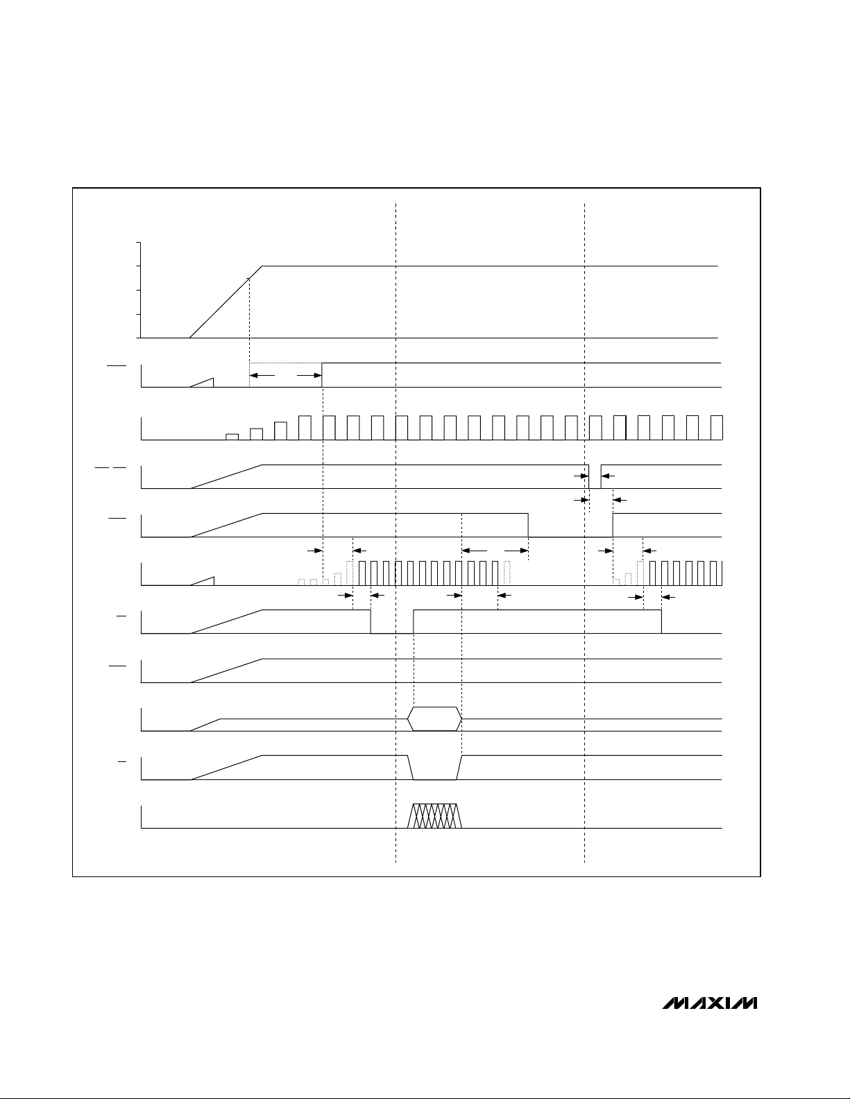
MAX1407/MAX1408/MAX1409/MAX1414
Low-Power, 16-Bit Multichannel DAS with
Internal Reference,10-Bit DACs, and RTC
38 ______________________________________________________________________________________
Dynamic Input Impedance
When designing with the MAX1407/MAX1408/
MAX1409/MAX1414, as with any other switched-capacitor ADC input, consider the advantages and disadvan-
tages of series input resistance. A series resistor
reduces the transient current impulse to the external
driving amplifier. This improves the amplifier phase
margin and reduces the possibility of ringing. The resis-
Figure 15. Initial Power-up, Sleep Mode, and Wake-Up Timing Diagram with AVDD>2.7V
4
AV
DD
RESET
(OPEN-DRAIN)
3
2
1
0v
HI
LO
2.7V
t
DSLP
WU1,WU2
SHDN
FOUT
(2.4576MHz)
INT
DRDY
DOUT
SCLK,
DIN
HI
LO
HI
LO
HI
LO
HI
LO
HI
LO
HI
LO
HI
THREE-STATED
LO
HI
CS
LO
HI
LO
t
DFON
t
DFI
SLEEP
WRITE
t
DFOF
t
DPD
t
WU
t
DPU
32kHz CLOCK
(INT. PULLUP)
INITIAL POWER-UP SLEEP MODE WAKE-UP
t
DFON
t
DFI

MAX1407/MAX1408/MAX1409/MAX1414
Low-Power, 16-Bit Multichannel DAS with
Internal Reference,10-Bit DACs, and RTC
______________________________________________________________________________________ 39
tor spreads the transient-load current from the sampler
over time due to the RC time constant of the circuit.
However, an improperly chosen series resistance can
hinder performance in high-resolution converters. The
settling time of the RC network can limit the speed at
which the converter can operate properly, or reduce
the settling accuracy of the sampler. In practice, this
means ensuring that the RC time constant, resulting
from the product of the driving source impedance and
the capacitance presented by both the device’s input
and any external capacitance is sufficiently small to
allow settling to the desired accuracy. Table 10 summarizes the maximum allowable series resistance vs.
external shunt capacitance for each different gain setting in order to ensure 16-bit performance in unbuffered
mode (for 60sps conversion rate).
Performing a Conversion or Offset-
Calibration with the ADC
Upon power-up, the MAX1407/MAX1408/MAX1409/
MAX1414 are in Standby mode. At this point, the ADC
register default settings are set for a normal ADC conversion (MODE = 0), conversion rate of 30Hz (RATE = 0),
gain of 1/3 V/V (GAIN [00]), input buffers bypassed and
powered down (BUFP = BUFN = 0), and unipolar mode
Table 9. Power States of Individual Blocks at Different Modes of Operation
x = powered-up
N/A = programming the parts into the wake-up mode would not alter the content of these blocks
Table 10. REXT, CEXT Values for Less than 16-Bit Gain Error in Unbuffered Mode
CIRCUIT BLOCKS
Serial Interface xxxx x
Wake-Up Circuitry xxxx x
Crystal Oscillator xxxx x
RTC with Alarm xxxx x
RESET Voltage Monitor xxxx x
Low VDD Voltage Monitor — xxx x
Master Bias Circuit — xxx x
PLL — xxx x
FOUT — xxx x
SHDN = High — xxx x
DAC1 —— x x N/A
DAC2 —— x x N/A
Bandgap —— x x N/A
Bandgap Buffer —— x x N/A
Signal Detect Comparator —— x x N/A
ADC Multiplexer —— x x N/A
ADC Input Buffers ——— x N/A
ADC ——— x N/A
SLEEP STANDBY IDLE RUN WA K E- U P EVEN T
POWER MODES
PGA GAIN
(V/V)
1 194 56 33 19 9
2 100 30 16 9 4.5
= 0pF C
C
EXT
EXT
EXTERNAL RESISTANCE R
= 50pF C
= 100pF C
EXT
EXT
(kΩ)
= 200pF C
EXT
EXT
= 500pF
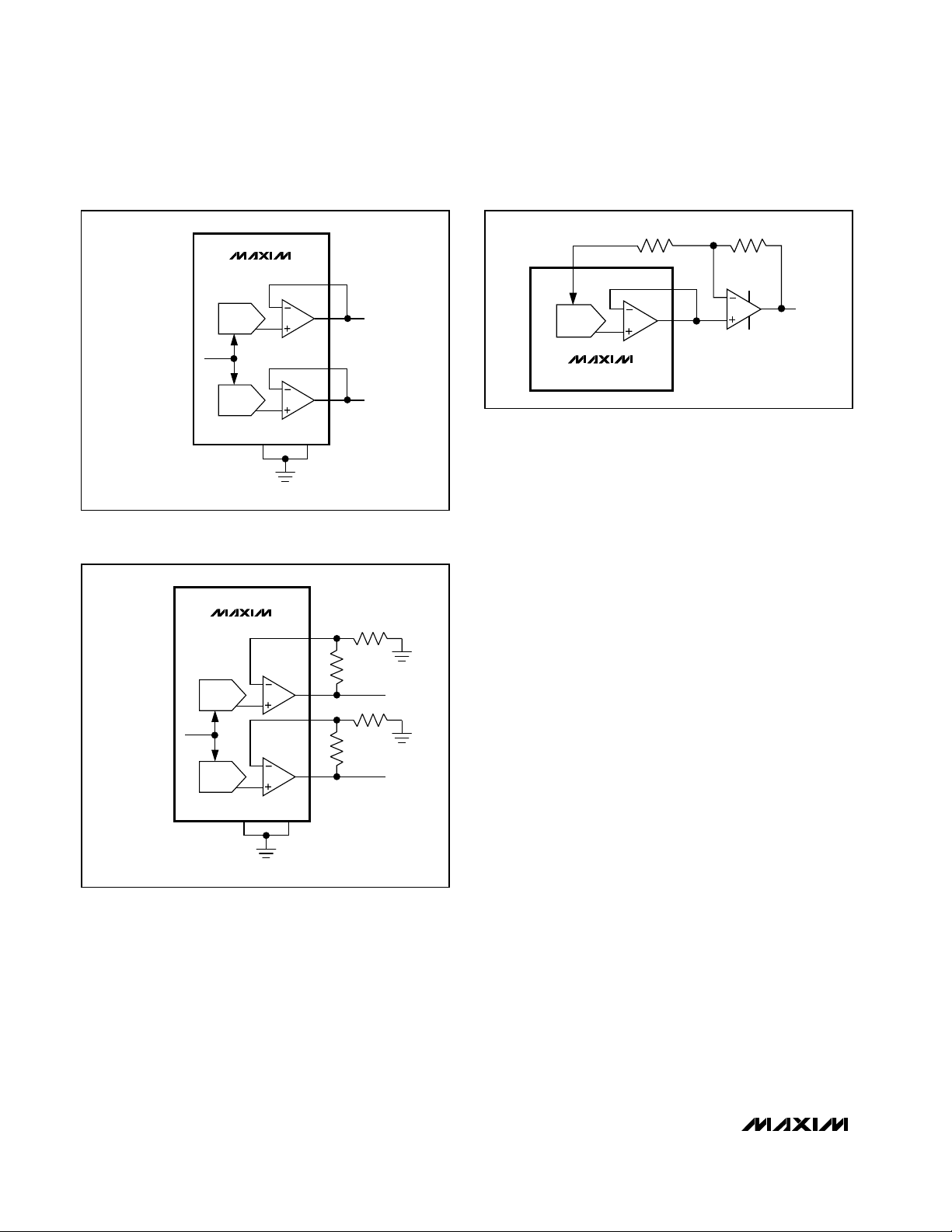
MAX1407/MAX1408/MAX1409/MAX1414
Low-Power, 16-Bit Multichannel DAS with
Internal Reference,10-Bit DACs, and RTC
40 ______________________________________________________________________________________
(BIP = 0). To initiate an ADC conversion: 1) Enter Run
mode by addressing the Run register 2) Select the
desired channels for conversion by writing to the MUX
register, (e.g., 94h selects IN1 for the positive channel
and IN2 for the negative channel) 3) Initiate the conversion by writing to the ADC register, (e.g., 01h). The first
conversion result becomes available in 100ms. The ADC
will keep doing conversions at a rate of 30Hz until powered down.
To perform an on-chip offset calibration on a specific
configuration, write to the ADC register with the MODE
bit and STA1 bit set to 1. The ADC will do one calibration using the inputs to the ADC specified in the MUX
register and then stop. The calibration result will be
stored in the Offset register in two’s complement form.
Subsequent ADC conversion results will have the offset
value subtracted before written to the DATA register.
The MODE bit will be reset to 0 automatically upon
completion of the calibration. The ADC is now ready for
a normal conversion.
The offset for a given ADC configuration can be stored
by the µP to avoid another ADC recalibration. Write the
stored offset back to the offset register when returning
back to that particular ADC configuration where the calibration was taken. Subsequent ADC conversion results
will have the offset value subtracted before they are
written to the DATA register.
DAC Unipolar Output
For a unipolar output, the output voltages and the reference have the same polarity. Figure 16 shows the
MAX1407/MAX1409/MAX1414s’ unipolar output circuit,
which is also the typical operating circuit for the DACs.
Table 11 lists some unipolar input codes and their corresponding output voltages.
For larger output swing see Figure 17. This circuit
shows the output amplifiers configured with a closedloop gain of +2V/V to provide 0 to 2.5V full-scale range
with the 1.25V reference.
DAC Bipolar Output
The MAX1407/MAX1409/MAX1414 DAC outputs can be
configured for bipolar operation using the application
circuit on Figure 18:
Figure 16. Unipolar Output Circuit
Figure 17. Unipolar Rail-to-Rail Output Circuit
Figure 18. Bipolar Output Circuit
R1 R2
MAX1407/MAX1409/MAX1414
DAC 1
REF
DAC 2
AGND
THE MAX1409 HAS ONE DAC
= 1.25V
V
REF
MAX1407/MAX1409/MAX1414
DAC 1
REF
DAC 2
AGND
DGND
DGND
FB1
FB2
FB1
FB2
10kΩ
10kΩ
10kΩ
10kΩ
OUT1
OUT2
OUT1
OUT2
REF
DAC_
MAX1407/MAX1409/MAX1414
FB_
OUT_
+5V
-5V
R2 = R1
V
OUT
THE MAX1409 HAS ONE DAC
= 1.25V
V
REF

MAX1407/MAX1408/MAX1409/MAX1414
Low-Power, 16-Bit Multichannel DAS with
Internal Reference,10-Bit DACs, and RTC
______________________________________________________________________________________ 41
Table 11. Unipolar Code Table
Table 12. Bipolar Code Table
Figure 19. Power-Supply Circuit Using MAX1833 Step-Up DC-DC Converter
Figure 20. Power-Supply Circuit Using MAX1759 Buck-Boost DC-DC Converter
DAC CONTENTS
MSB LSB
1111 1111 11 +V
1000 0000 01 +V
1000 0000 00 +V
0111 1111 11 +V
0000 0000 01 +V
ANALOG OUTPUT
(1023/1024)
REF
(513/1024)
REF
(512/1024) = +V
REF
(511/1024)
REF
REF
0000 0000 00 0
10µH
V
BAT
LX
MAX1833
BATT
E1*
OUT
RST
SHDN
GND
10µF
(1/1024)
/2
REF
= 3.3V OR V
V
DD
10µF
18nF
CPLL
SHDN
IN0
AGND DGND
DAC CONTENTS
MSB LSB
1111 1111 11 +V
1000 0000 01 +V
1000 0000 00 0
0111 1111 11 -V
0000 0000 01 -V
0000 0000 00 -V
BAT
0.1µF 0.1µF
AV
DD
MAX1407
MAX1408
MAX1414
DV
DD
RESET RESET
INPUTWU1
ANALOG OUTPUT
(511/512)
REF
(1/512)
REF
(1/512)
REF
(511/512)
REF
(512/512) = -V
REF
0.1µF
V
DD
µP/µC
V
SS
REF
*ONE Li+ COIN, TWO ALKALINE, OR TWO BUTTON CELLS
0.33µF
CXN CXP
IN
V
E1*
BAT
*ONE Li+ COIN, ONE Li+, 2-3 ALKALINE, 2-3 NIMH, OR 2-3 BUTTON CELLS
MAX1759
GNDFB PGND
10µF
OUT
POK
SHDN
R
R
= 3.3V
V
DD
10µF
18nF
CPLL
SHDN
IN0
AGND DGND
AV
DD
MAX1407
MAX1408
MAX1414
0.1µF 0.1µF
DV
DD
RESET RESET
0.1µF
V
DD
µP/µC
INPUTWU1
V
SS

MAX1407/MAX1408/MAX1409/MAX1414
Low-Power, 16-Bit Multichannel DAS with
Internal Reference,10-Bit DACs, and RTC
42 ______________________________________________________________________________________
where NB is the decimal value of the DAC’s binary
input code. Table 12 shows digital codes (offset binary)
and corresponding output voltages for Figure 18
assuming R1 = R2.
Power Supplies
Power to the MAX1407/MAX1408/MAX1409/MAX1414
family can be supplied in a number of ways. Figures 19,
20, 21, and 22 are power-supply circuits using a step-up
converter, buck-boost converter, step-down converter,
and a direct battery, respectively. Choose the correct
power-supply circuit for your specific application.
Connect the MAX1407/MAX1408/MAX1409/MAX1414
AVDDand DVDDpower supplies together. While the
latch-up performance of the MAX1407/MAX1408/
MAX1409/MAX1414 is adequate, it is important that
power is applied to the device before the analog input
signals (IN_) to avoid latch-up. If this is not possible,
limit the current flow into any of these pins to 50mA.
Electrochemical Sensor Operation
The MAX1407/MAX1408/MAX1409/MAX1414 family interface with electrochemical sensors. The 10-bit DACs with
the force/sense buffers have the flexibility to connect to
many different types of sensors. Figure 23 shows how to
interface with a two electrode potentiostat. A single DAC
is required to set the bias across the sensor relative to
ground and an external precision resistor completes the
transimpedance amplifier configuration to convert the
current generated by the sensor to a voltage to be measured by the ADC. The induced error from this source is
negligible due to FB1’s extremely low input bias current.
Internally, the ADC can differentially measure directly
across the external transimpedance resistor, RF, eliminating any errors due to voltages drifting over time, temperature, or supply voltage. Figure 24 shows a two electrode
potentiostat application that is driven at the working electrode and measured at the counter electrode. With this
application, the DAC connected to the working electrode
is configured in unity gain and the DAC connected to the
Figure 21. Power-Supply Circuit Using MAX640 Step-Down DC-DC Converter
Figure 22. Power-Supply Circuit Using Direct Battery Connection
100µH
V+
MAX640
SHDN
VFBLBI GND
V
BAT
E1*
*ONE TRANSISTOR (9V), ONE J CELL (6V), OR FOUR ALKALINE CELLS
33µF
LX
D1
VOUT
2R
R
VDD (+3.3V)
100µF
IN0
18nF
CPLL
AV
DD
MAX1407
MAX1408
MAX1409
MAX1414
AGND DGND
0.1µF 0.1µF
DV
DD
RESET RESET
WU1 INPUT
E1*
10µF
18nF
V
BAT
0.1µF
0.1µF
0.1µF
CPLL
AV
DD
MAX1407
MAX1408
MAX1409
MAX1414
AGND DGND
DV
DD
RESET RESET
WU1 INPUT
V
DD
µP/µC
V
SS
*ONE Li+ COIN OR TWO BUTTON CELLS
VV
=
OUT REF
2
1024
NB
−
1
V
DD
µP/µC
V
SS
0.1µF

MAX1407/MAX1408/MAX1409/MAX1414
Low-Power, 16-Bit Multichannel DAS with
Internal Reference,10-Bit DACs, and RTC
______________________________________________________________________________________ 43
counter electrode is configured as a transimpedance
amplifier to measure the current. Figure 25 shows a three
electrode potentiostat application that is driven at all the
electrodes and measured at the working electrode. With
this application, the DAC connected to the working elec-
trode sets the bias voltage relative to the reference electrode and also measures the current that the sensor produces. The DAC connected to the reference and counter
electrodes takes advantage of the force/sense outputs to
Figure 23. Self-Biased Two Electrode Potentiostat Application
Figure 24. Driven Two Electrode Potentiostat Application
Figure 25. Driven Three Electrode Potentiostat Application
Figure 26. Optical Reflectometry Application
MAX1407
MAX1409
MAX1414
REF
10-BIT DAC
AUX.
VOLTAGE
INPUTS
ALL I/O AVAILABLE AS INPUTS TO ADC AND COMPARATOR.
MAX1409 HAS IN0, OUT1, FB1, AND REF ONLY.
IN0
IN1
IN2
IN3
BAND
GAP
BUF
OUT1
FB1
REF
4.7µF
F
I
SENSOR
F
R
WE
CE
MAX1407
MAX1414
REF
10-BIT DAC
AUX.
VOLTAGE
INPUTS
ALL I/O AVAILABLE AS INPUTS TO ADC AND COMPARATOR.
IN0
IN1
IN2
IN3
REF
10-BIT DAC
BAND
GAP
BUF
OUT1
FB1
FB2
OUT2
REF
4.7µF
F
F
R
I
WE
RE
CE
SENSOR
MAX1407
MAX1414
REF
10-BIT DAC
AUX.
VOLTAGE
INPUTS
ALL I/O AVAILABLE AS INPUTS TO ADC AND COMPARATOR.
IN0
IN1
IN2
IN3
REF
10-BIT DAC
BAND
GAP
BUF
OUT1
FB1
OUT2
FB2
REF
4.7µF
F
I
SENSOR
F
R
WE
CE
V
IFR
4.7µF
BAT
LED
QB
B
R
F
PHOTODIODE
MAX1407
MAX1414
REF
10-BIT DAC
REF
10-BIT DAC
AUX.
VOLTAGE
INPUTS
ALL I/O AVAILABLE AS INPUTS TO ADC AND COMPARATOR.
IN0
IN1
IN2
IN3
BAND
GAP
BUF
OUT1
FB1
OUT2
FB2
REF

MAX1407/MAX1408/MAX1409/MAX1414
Low-Power, 16-Bit Multichannel DAS with
Internal Reference,10-Bit DACs, and RTC
44 ______________________________________________________________________________________
maintain the reference electrode bias voltage by virtue of
the feedback path through the sensor.
Optical Reflectometry
Figure 26 illustrates the MAX1407/MAX1414 in an optical
reflectometry application. The first DAC is used with an
external transistor to set the bias current through the LED
and the second DAC is used to properly bias and convert
the photodiode current to a voltage measured by the
ADC. The low input bias current into the DAC feedback
pin (FB2) allows the measurement of very small currents.
The DACs provide the flexibility in setting an accurate
and stable LED current and adjusting the bias across the
photodiode. Set the LED bias current externally if the
MAX1409 is used in this application.
Thermistor Measurement
A thermistor connected in a half-bridge configuration
as shown in Figure 27 is used to measure temperatures
very accurately with the MAX1407/MAX1408/
MAX1409/MAX1414. The internal reference drives the
thermistor as well as the ADC, so the reference variation is cancelled out when calculating the temperature.
The only significant errors are from the RLresistor and
the thermistor itself. The ADC performs a unipolar conversion with the PGA set to a gain of 1V/V.
Figure 27. Thermistor Application Circuit
MAX1407
MAX1408
MAX1409
MAX1414
REF
DRDY NOT AVAILABLE ON THE MAX1409
BAND
GAP
WAKE-UP
INTERRUPT
GENERATOR
REF
DRDY
INT
R
L
R
T
AGND
4.7µF
BUF
8:1
MUX
16b ADC
CMP
REF
IN0
8:1
MUX
Figure 28. Thermocouple Application Circuit
MAX1407
MAX1408
MAX1414
REF
C
C
BAND
GAP
WAKE-UP
INTERRUPT
GENERATOR
REF
DRDY
INT
R
R
4.7µF
BUF
8:1
MUX
16b ADC
CMP
AGND
THERMOCOUPLE
JUNCTION
IN1
IN0
IN2
8:1
MUX
CJC

MAX1407/MAX1408/MAX1409/MAX1414
Low-Power, 16-Bit Multichannel DAS with
Internal Reference,10-Bit DACs, and RTC
______________________________________________________________________________________ 45
Thermocouple Measurement
Figure 28 shows a thermocouple connected to the differential inputs of the MAX1407/MAX1408/MAX1409/
MAX1414. In this application, the internal buffers are
enabled to allow for the decoupling shown at the input.
The decoupling eliminates noise pickup from the thermocouple. With the internal buffers enabled, the input
common-mode range is reduced so the IN2 input is
biased to the internal reference voltage at +1.25V. When
the buffer is enabled, the IN1 input is limited to +1.4V.
Strain-Gauge Operation
Connect the differential inputs of the MAX1407/
MAX1408/MAX1409/MAX1414 to the bridge network of
the strain gauge as shown in Figure 29. When connected to the internal reference, the ADC can resolve below
10µV at the differential inputs. The internal buffers provide a high input impedance as long as the signal is
within the reduced common-mode range of the input
buffers. The bridge may also be driven directly from the
supply voltage. In this configuration, the ADC first measures the supply voltage and then the differential input
in sequence, and then calculates the ratio.
Grounding and Layout
For best performance, use printed circuit boards with
separate analog and digital ground planes. The device
perfomance will be highly degraded when using wirewrap boards.
Design the printed circuit board so that the analog and
digital sections are separated and confined to different
areas of the board. Join the digital and analog ground
planes at one point. If the MAX1407/MAX1408/
MAX1409/MAX1414 is the only device requiring an
AGND to DGND connection, then the ground planes
should be connected at the AGND pin of the MAX1407/
MAX1408/MAX1409/MAX1414. In systems where multiple devices require AGND to DGND connections, the
connection should still be made at only one point. Make
the star ground as close to the MAX1407/MAX1408/
MAX1409/MAX1414 as possible.
Avoid running digital lines under the device because
these may couple noise onto the die. Run the analog
ground plane under the MAX1407/MAX1408/
MAX1409/MAX1414 to minimize coupling of digital
noise. Make the power-supply lines to the MAX1407/
MAX1408/MAX1409/MAX1414 as wide as possible to
provide low-impedance paths and reduce the effects of
glitches on the power-supply line.
Shield fast switching signals such as clocks with digital
ground to avoid radiating noise to other sections of the
board. Avoid running clock signals near the analog
inputs. Avoid crossover of digital and analog signals.
Traces on opposite sides of the board should run at
right angles to each other. This will reduce the effects
of feedthrough on the board. A microstrip technique is
best, but is not always possible with double-sided
boards. In this technique, the component side of the
board is dedicated to ground planes while signals are
placed on the solder side.
Good coupling is important when using high-resolution
ADCs. Decouple all analog supplies with 1µF capacitors in parallel with 0.1µF HF ceramic capacitors to
AGND. Place these components as close to the device
as possible to achieve the best decoupling.
Crystal Layout
Since it is possible for noise to be coupled onto the
crystal pins, care must be taken when placing the
external crystal on a PC board layout. It is very important to follow a few basic layout guidelines concerning
Figure 29. Strain-Gauge Application Circuit
REF OR AV
DD
R
A
R
D
R
B
R
C
IN0
IN1
DRDY NOT AVAILABLE ON THE MAX1409
8:1
MUX
8:1
MUX
MAX1407
MAX1408
MAX1414
REF
16-BIT ADC
CMP
WAKE-UP
BAND
GAP
INTERRUPT
GENERATOR
BUF
DRDY
INT
REF
4.7µF

MAX1407/MAX1408/MAX1409/MAX1414
Low-Power, 16-Bit Multichannel DAS with
Internal Reference,10-Bit DACs, and RTC
46 ______________________________________________________________________________________
the placement of the crystal on the PC board layout to
insure that extra clock “ticks” do not couple onto the
crystal pins.
1) It is important to place the crystal as close as possi-
ble to the CLKIN and CLKOUT pins. Keeping the
trace lengths between the crystal and pins as small
as possible reduces the probability of noise coupling by reducing the length of the “antennae”.
Keeping the trace lengths small also decreases the
amount of stray capacitance.
2) Keep the crystal bond pads and trace width to the
CLKIN and CLKOUT pins as small as possible. The
larger these bond pads and traces are, the more
likely it is that noise can couple from adjacent signals.
3) If possible, place a guard ring (connect to ground)
around the crystal. This helps to isolate the crystal
from noise coupled from adjacent signals.
4) Insure that no signals on other PC board layers run
directly below the crystal or below the traces to the
CLKIN and CLKOUT pins. The more the crystal is
isolated from other signals on the board, the less
likely it is that noise will be coupled into the crystal.
There should be a minimum of 0.200 inches
between any digital signal and any trace connected
to CLKIN or CLKOUT.
5) It may also be helpful to place a local ground plane
on the PC board layer immediately below the crystal
guard ring. This helps to isolate the crystal from
noise coupling from signals on other PC board layers. Note: The ground plane needs to be in the
vicinity of the crystal only and not on the entire
board.
Definitions
Integral Nonlinearity
Integral nonlinearity (INL) is the deviation of the values
on an actual transfer function (with offset and gain error
removed) from a straight line. This straight line can be
either a best straight-line fit or a line drawn between the
endpoints of the transfer function, once offset and gain
errors have been nullified. The static linearity parameters for the MAX1407/MAX1408/MAX1409/MAX1414 are
measured using the endpoint method.
Differential Nonlinearity
Differential nonlinearity (DNL) is the difference between
an actual step width and the ideal value of 1LSB. A
DNL error specification of less than 1LSB guarantees
no missing codes and a monotonic transfer function.
Pin Configurations (continued)
TOP VIEW
1
1
IN7
2
DO
3
IN6
4
IN4
5
IN0
6
REF
AGND
AV
CPLL
WU1
WU2
RESET
IN1
IN2
7
MAX1408
8
DD
9
10
11
12
13
14
28
27
26
25
24
23
22
21
20
19
18
17
16
15
IN5
IN3
DV
DD
DGND
CS
SCLK
DIN
DOUT
INT
CLKIN
CLKOUT
FOUT
DRDY
SHDN
FB1
OUT1
IN0
AGND
AV
CPLL
WU1
WU2
RESET
2
3
4
MAX1409
5
6
DD
7
8
9
10
20
19
18
17
16
15
14
13
12
11
DV
DD
DGND
CS
SCLKREF
DIN
DOUT
INT
CLKIN
CLKOUT
FOUT

MAX1407/MAX1408/MAX1409/MAX1414
Low-Power, 16-Bit Multichannel DAS with
Internal Reference,10-Bit DACs, and RTC
______________________________________________________________________________________ 47
Typical Operating Circuit
LX
CONVERTER
BATT
V
BAT
DC-DC
GND
SENSOR
OUT
RST
SHDN
CPLL
AV
DD
SHDN
IN0
REF
IN1
MAX1407
MAX1414
OUT1
FB1
WE
RE
CE
FB2
OUT2
AGND DGND
DV
DD
RESET
CLKIN
CLKOUT
FOUT
CS
SCLK
DIN
DOUT
INT
DRDY
WU1 I/O
WU2 I/O
RESET
CLKIN
OUTPUT
SCK
MOSI
MISO
INPUT
INPUT
V
DD
µP/µC
V
SS

MAX1407/MAX1408/MAX1409/MAX1414
Low-Power, 16-Bit Multichannel DAS with
Internal Reference,10-Bit DACs, and RTC
Maxim cannot assume responsibility for use of any circuitry other than circuitry entirely embodied in a Maxim product. No circuit patent licenses are
implied. Maxim reserves the right to change the circuitry and specifications without notice at any time.
48 ____________________Maxim Integrated Products, 120 San Gabriel Drive, Sunnyvale, CA 94086 408-737-7600
© 2001 Maxim Integrated Products Printed USA is a registered trademark of Maxim Integrated Products.
Package Information
SSOP.EPS
 Loading...