

General Description
The MAX1393/MAX1396 micropower, serial-output, 12bit, analog-to-digital converters (ADCs) operate with a
single power supply from +1.5V to +3.6V. These ADCs
feature automatic shutdown, fast wake-up, and a highspeed 3-wire interface. Power consumption is only
0.734mW (VDD= +1.5V) at the maximum conversion rate
of 312.5ksps. AutoShutdown™ between conversions
reduces power consumption at slower throughput rates.
The MAX1393/MAX1396 require an external reference
V
REF
that has a wide range from 0.6V to VDD. The
MAX1393 provides one true-differential analog input
that accepts signals ranging from 0 to V
REF
(unipolar
mode) or ±V
REF
/2 (bipolar mode). The MAX1396 provides two single-ended inputs that accept signals ranging from 0 to V
REF
. Analog conversion results are
available through a 5MHz 3-wire SPI™-/QSPI™-/
MICROWIRE™-/digital signal processor (DSP)-compatible serial interface. Excellent dynamic performance,
low voltage, low power, ease of use, and small package sizes make these converters ideal for portable battery-powered data-acquisition applications, and for
other applications that demand low power consumption
and minimal space.
The MAX1393/MAX1396 are available in a space-saving
(3mm x 3mm) 10-pin TDFN package or 10-pin µMAX
®
package. The parts operate over the extended (-40°C to
+85°C) and military (-55°C to +125°C) temperature ranges.
Applications
Portable Datalogging
Data Acquisition
Medical Instruments
Battery-Powered Instruments
Process Control
Features
♦ 312.5ksps, 12-Bit Successive-Approximation
Register (SAR) ADCs
♦ Single True-Differential Analog Input Channel
with Unipolar-/Bipolar-Select Input (MAX1393)
♦ Dual Single-Ended Input Channel with Channel-
Select Input (MAX1396)
♦ ±1 LSB INL, ±1 LSB DNL, No Missing Codes
♦ ±2 LSB Total Unadjusted Error (TUE)
♦ 70dB SINAD at 75kHz Input Frequency
♦ External Reference (0.6V to V
DD
)
♦ Single-Supply Voltage (+1.5V to +3.6V)
♦ 0.915mW at 300ksps, 1.8V
♦ 0.305mW at 100ksps, 1.8V
♦ 3.1µW at 1ksps, 1.8V
♦ < 1µA Shutdown Current
♦ AutoShutdown Between Conversions
♦ SPI-/QSPI-/MICROWIRE-/DSP-Compatible,
3- or 4-Wire Serial Interface
♦ Small (3mm x 3mm) 10-Pin TDFN or µMAX
(3mm x 5mm) Package
MAX1393/MAX1396
1.5V to 3.6V, 312.5ksps, 1-Channel True-Differential/
2-Channel Single-Ended, 12-Bit, SAR ADCs
________________________________________________________________ Maxim Integrated Products 1
19-3644; Rev 0; 5/05
For pricing, delivery, and ordering information, please contact Maxim/Dallas Direct! at
1-888-629-4642, or visit Maxim’s website at www.maxim-ic.com.
PART TEMP RANGE PIN-PACKAGE ANALOG INPUTS TOP MARK
MAX1393ETB -40°C to +85°C 10 TDFN-EP** 1-CH DIFF AOZ
MAX1393EUB -40°C to +85°C 10 µMAX 1-CH DIFF —
MAX1393MTB* -55°C to +125°C 10 TDFN-EP** 1-CH DIFF —
MAX1393MUB* -55°C to +125°C 10 µMAX 1-CH DIFF —
MAX1396ETB -40°C to +85°C 10 TDFN-EP** 2-CH S/E APC
MAX1396EUB* -40°C to +85°C 10 µMAX 2-CH S/E —
MAX1396MTB* -55°C to +125°C 10 TDFN-EP** 2-CH S/E —
MAX1396MUB* -55°C to +125°C 10 µMAX 2-CH S/E —
AutoShutdown is a trademark of Maxim Integrated Products, Inc.
SPI/QSPI are trademarks of Motorola, Inc.
MICROWIRE is a trademark of National Semiconductor Corp.
µMAX is a registered trademark of Maxim Integrated Products, Inc.
Typical Operating Circuit and Pin Configurations appear at
end of data sheet.
*Future product—contact factory for availability.
**EP = Exposed pad.
查询MAX1393供应商
MAX1393/MAX1396
2 _______________________________________________________________________________________
1.5V to 3.6V, 312.5ksps, 1-Channel True-Differential/
2-Channel Single-Ended, 12-Bit, SAR ADCs
ABSOLUTE MAXIMUM RATINGS
ELECTRICAL CHARACTERISTICS
(V
DD
= +1.5V to +3.6V, V
REF
= VDD, C
REF
= 0.1µF, f
SCLK
= 5MHz, TA= T
MIN
to T
MAX
, unless otherwise noted. Typical values are at
T
A
= +25°C.)
Stresses beyond those listed under “Absolute Maximum Ratings” may cause permanent damage to the device. These are stress ratings only, and functional
operation of the device at these or any other conditions beyond those indicated in the operational sections of the specifications is not implied. Exposure to
absolute maximum rating conditions for extended periods may affect device reliability.
VDDto GND..............................................................-0.3V to +4V
SCLK,
CS, OE, CH1/CH2, UNI/BIP,
DOUT to GND.........................................-0.3V to (V
DD
+ 0.3V)
AIN+, AIN-, AIN1, AIN2, REF to GND ........-0.3V to (V
DD
+ 0.3V)
Maximum Current into Any Pin .........................................±50mA
Continuous Power Dissipation (T
A
= +70°C)
10-Pin TDFN (derate 18.5mW/°C above +70°C) ....1481.5mW
10-Pin µMAX (derate 5.6mW/°C above +70°C) ........444.4mW
Operating Temperature Ranges
MAX139_E_ _...................................................-40°C to +85°C
MAX139_M_ _................................................-55°C to +125°C
Junction Temperature......................................................+150°C
Storage Temperature Range .............................-60°C to +150°C
Lead Temperature (soldering, 10s) .................................+300°C
PARAMETER
CONDITIONS
UNITS
DC ACCURACY (Note 1)
Resolution 12 Bits
Integral Nonlinearity INL ±1 LSB
Differential Nonlinearity DNL No missing code overtemperature ±1 LSB
Offset Error 0.5 ±2 LSB
Gain Error Offset nulled 0.5 ±2 LSB
Total Unadjusted Error TUE ±2 LSB
Offset-Error Temperature
Coefficient
LSB/°C
Gain-Error Temperature
Coefficient
LSB/°C
Channel-to-Channel Offset
Matching
MAX1396 only
LSB
Channel-to-Channel Gain
Matching
MAX1396 only
LSB
Input Common-Mode Rejection CMR VCM = 0 to VDD, MAX1393 only
mV/V
DYNAMIC SPECIFICATIONS (Note 2)
V
REF
= VDD = 1.6 70
V
REF
= VDD = 1.8–2.5 69Signal-to-Noise Plus Distortion SINAD
V
REF
= VDD = 2.5–3.6 70
dB
V
REF
= VDD = 1.6
V
REF
= VDD = 1.8–2.5 70 71
Signal-to-Noise Ratio SNR
V
REF
= VDD = 2.5–3.6 71
dB
Total Harmonic Distortion THD -83 -75 dBc
Spurious-Free Dynamic Range SFDR -85 -76 dBc
Intermodulation Distortion IMD
f
IN1
= 73kHz at -6.5dBFS,
f
IN2
= 77kHz at -6.5dBFS
-78 dB
Channel-to-Channel Crosstalk MAX1396 only -70 dB
SYMBOL
MIN TYP MAX
±0.004
±0.001
±0.1
±0.1
±0.1
70.5
MAX1393/MAX1396
_______________________________________________________________________________________ 3
1.5V to 3.6V, 312.5ksps, 1-Channel True-Differential/
2-Channel Single-Ended, 12-Bit, SAR ADCs
ELECTRICAL CHARACTERISTICS (continued)
(V
DD
= +1.5V to +3.6V, V
REF
= VDD, C
REF
= 0.1µF, f
SCLK
= 5MHz, TA= T
MIN
to T
MAX
, unless otherwise noted. Typical values are at
T
A
= +25°C.)
PARAMETER
SYMBOL
CONDITIONS
MIN
TYP
MAX
UNITS
Full-Power Bandwidth -3dB point 4
MHz
MAX1393
Full-Linear Bandwidth SINAD > 68dB
MAX1396
kHz
CONVERSION RATE
Conversion Time t
CONV
13 clock cycles 2.6 µs
Throughput Rate
16 clock cycles per conversion; includes
ksps
Power-Up and Acquisition Time t
ACQ
Three SCLK cycles
ns
Aperture Delay t
AD
8ns
Aperture Jitter t
AJ
30 ps
Serial Clock Frequency f
CLK
0.1 5.0
MHz
ANALOG INPUTS (AIN+, AIN-, AIN1, AIN2)
Unipolar 0
Input Voltage Range V
IN
Bipolar, MAX1393 only, (AIN+ - AIN-)
V
Common-Mode Input Voltage
Range
V
CM
0
V
Input Leakage Current
Channel not selected, or conversion
stopped, or in shutdown mode
±1 µA
Input Capacitance 16 pF
REFERENCE INPUT (REF)
REF Input Voltage Range V
REF
0.6
V
DD
+
V
REF Input Capacitance 24 pF
REF DC Leakage Current
µA
REF Input Dynamic Current 312.5ksps 20 60 µA
DIGITAL INPUTS (SCLK, CS, OE, CH1/CH2, UNI/BIP)
Input-Voltage Low V
IL
0.3 x
V
Input-Voltage High V
IH
0.7 x
V
Input Hysteresis
0.06 x
V
Input Leakage Current I
IL
Inputs at GND or V
DD
±1 µA
CS, OE 1
Input Capacitance C
IN
CH1/CH2, UNI/BIP
pF
DIGITAL OUTPUT (DOUT)
Output-Voltage Low V
OL
I
SINK
= 2mA
0.1 x
V
Output-Voltage High V
OH
I
SOURCE
= 2mA
0.9 x
V
200
150
power-up, acquisition, and conversion time
600
-V
/2 +V
REF
Bipolar, MAX1393 only, [(AIN+) + (AIN-)] / 2
V
DD
0.025 ±2.5
V
DD
312.5
V
REF
REF
V
DD
0.05
V
DD
/2
V
DD
12.5
V
DD
MAX1393/MAX1396
4 _______________________________________________________________________________________
1.5V to 3.6V, 312.5ksps, 1-Channel True-Differential/
2-Channel Single-Ended, 12-Bit, SAR ADCs
ELECTRICAL CHARACTERISTICS (continued)
(V
DD
= +1.5V to +3.6V, V
REF
= VDD, C
REF
= 0.1µF, f
SCLK
= 5MHz, TA= T
MIN
to T
MAX
, unless otherwise noted. Typical values are at
T
A
= +25°C.)
PARAMETER
CONDITIONS
UNITS
Tri-State Leakage Current I
LT
OE = V
DD
±1 µA
Tri-State Output Capacitance C
OUT
OE = V
DD
10 pF
POWER SUPPLY
Positive Supply Voltage V
DD
1.5 3.6 V
VDD = 1.6V
200
f
SAMPLE
= 100ksps
V
DD
= 3V
260
VDD = 1.6V
600
f
SAMPLE
= 312.5ksps
V
DD
= 3V
800
Power-down mode (Note 4) 5 10
Positive Supply Current (Note 3) I
DD
Power-down mode (Note 5) 0.2
µA
Power-Supply Rejection PSR
µV/V
TIMING CHARACTERISTICS
(V
DD
= +1.5V to +3.6V, V
REF
= VDD, C
REF
= 0.1µF, f
SCLK
= 5MHz, TA= T
MIN
to T
MAX
, unless otherwise noted. Typical values are at
T
A
= +25°C.) (Figure 1)
PARAMETER
CONDITIONS
SCLK Clock Period t
CP
ns
SCLK Pulse-Width High t
CH
90 ns
SCLK Pulse-Width Low t
CL
90 ns
CS Fall to SCLK Rise Setup t
CSS
80 ns
SCLK Rise to CS Fall Ignore t
CSO
0ns
SCLK Fall to DOUT Valid t
DOV
C
LOAD
= 0 to 30pF 10 80 ns
OE Rise to DOUT Disable t
DOD
620ns
OE Fall to DOUT Enable t
DOE
920ns
CS Pulse-Width High or Low t
CSW
80 ns
OE Pulse-Width High or Low t
OEW
80 ns
CH1/CH2 Setup Time (to the
First SCLK)
t
CHS
MAX1396 only 10 ns
CH1/CH2 Hold Time (to the First
SCLK)
t
CHH
MAX1396 only 0 ns
UNI/BIP Setup Time (to the First
SCLK)
t
UBS
MAX1393 only 10 ns
UNI/BIP Hold Time (to the First
SCLK)
t
UBH
MAX1393 only 0 ns
Note 1: V
DD
= 1.5V, V
REF
= 1.5V, and V
AIN
= 1.5V.
Note 2: V
DD
= 1.5V, V
REF
= 1.5V, V
AIN
= 1.5V
P-P
, f
SCLK
= 5MHz, f
SAMPLE
= 312.5ksps, and fIN(sine wave) = 75kHz.
Note 3: All digital inputs swing between V
DD
and GND. V
REF
= VDD,fIN= 75kHz sine wave, V
AIN
= V
REFP-P,CLOAD
= 30pF on DOUT.
Note 4: CS = V
DD
, OE = UNI/BIP = CH1/CH2 = VDDor GND, SCLK is active.
Note 5: CS = V
DD
, OE = UNI/BIP = CH1/CH2 = VDDor GND, SCLK is inactive.
Note 6: Change in V
AIN
at code boundary 4094.5.
SYMBOL
MIN TYP MAX
176
225
520
710
±2.5
VDD = 1.5V to 3.6V, full-scale input (Note 6) ±150 ±1000
SYMBOL
MIN TYP MAX UNITS
200 10,000
MAX1393/MAX1396
_______________________________________________________________________________________ 5
1.5V to 3.6V, 312.5ksps, 1-Channel True-Differential/
2-Channel Single-Ended, 12-Bit, SAR ADCs
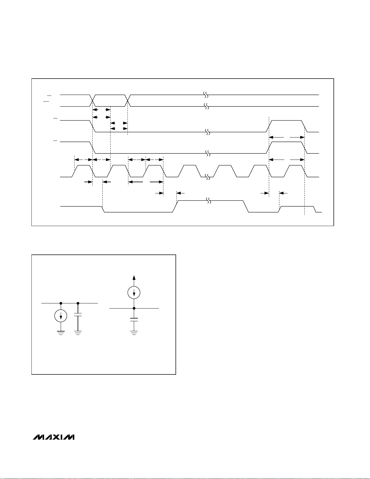
CS
SCLK
DOUT
OE
UNI/BIP OR
CH1/CH2
t
UBS
t
CHS
t
UBH
t
CHH
t
CSO
t
CSS
t
CL
t
CH
t
CP
t
DOE
HIGH-Z
t
DOV
t
OEW
t
CSW
t
DOD
HIGH-Z
Figure 1. Detailed Serial-Interface Timing Diagram
GND
50pF
50pF
DOUT
DOUT
GND
V
DD
a) HIGH IMPEDANCE TO VOH, V
OL
TO VOH,
AND V
OH
TO HIGH IMPEDANCE
b) HIGH IMPEDANCE TO V
OL, VOH
TO VOL,
AND V
OL
TO HIGH IMPEDANCE
10mA
10mA
Figure 2. Load Circuits for Enable/Disable Times
1.5V to 3.6V, 312.5ksps, 1-Channel True-Differential/
2-Channel Single-Ended, 12-Bit, SAR ADCs
MAX1393/MAX1396
6 _______________________________________________________________________________________
DNL ERROR vs. REFERENCE VOLTAGE
MAX1393/96 toc04
REFERENCE VOLTAGE (V)
DNL ERROR (LSB)
3.12.62.11.61.1
-0.8
-0.6
-0.4
-0.2
0
0.2
0.4
0.6
0.8
1.0
-1.0
0.6 3.6
VDD = 3.6V
MAX DNL
MIN DNL
OFFSET ERROR vs. SUPPLY VOLTAGE
MAX1393/96 toc05
SUPPLY VOLTAGE (V)
OFFSET ERROR (µV)
V
REF
= 1.5V
TEMPERATURE = +25°C
-300
-200
-100
0
100
200
300
400
-400
3.33.01.8 2.1 2.4 2.71.5 3.6
AIN1
AIN2
OFFSET ERROR vs. TEMPERATURE
MAX1393/96 toc06
TEMPERATURE (°C)
OFFSET ERROR (µV)
95-25 5 35 65
-300
-200
-100
0
100
200
300
400
-400
-55 125
VDD = 2.6V
OFFSET ERROR
vs. REFERENCE VOLTAGE
MAX1393/96 toc07
REFERENCE VOLTAGE (V)
OFFSET ERROR (µV)
3.11.1 1.6 2.1 2.6
-300
-200
-100
0
100
200
300
400
-400
0.6 3.6
VDD = 3.6V
GAIN ERROR vs. SUPPLY VOLTAGE
MAX1393/96 toc08
SUPPLY VOLTAGE (V)
GAIN ERROR (µV)
3.33.01.8 2.1 2.4 2.7
-300
-200
-100
0
100
200
300
400
-400
1.5 3.6
V
REF
= 1.5V
TEMPERATURE = +25°C
GAIN ERROR vs. TEMPERATURE
MAX1393/96 toc09
TEMPERATURE (°C)
GAIN ERROR (µV)
95-25 5 35 65
-300
-200
-100
0
100
200
300
400
-400
-55 125
VDD = 2.6V
AIN1
AIN2
Typical Operating Characteristics
(VDD= +1.5V, V
REF
= +1.5V, C
REF
= 0.1µF, CL= 30pF, f
SCLK
= 5MHz. TA= +25°C, unless otherwise noted.)
INL vs. CODE
MAX1393/96 toc01
CODE
INL (LSB)
358430722048 25601024 1536512
-0.8
-0.6
-0.4
-0.2
0
0.2
0.4
0.6
0.8
1.0
-1.0
0 4096
VDD = 1.5V
V
REF
= 1.5V
INL ERROR vs. REFERENCE VOLTAGE
MAX1393/96 toc02
REFERENCE VOLTAGE (V)
INL ERROR (LSB)
3.12.62.11.61.1
-0.8
-0.6
-0.4
-0.2
0
0.2
0.4
0.6
0.8
1.0
-1.0
0.6 3.6
VDD = 3.6V
MAX INL
MIN INL
DNL vs. CODE
MAX1393/96 toc03
CODE
DNL (LSB)
358430722048 25601024 1536512
-0.8
-0.6
-0.4
-0.2
0
0.2
0.4
0.6
0.8
1.0
-1.0
0 4096
VDD = 1.5V
V
REF
= 1.5V

MAX1393/MAX1396
_______________________________________________________________________________________ 7
SUPPLY CURRENT
vs. CONVERSION RATE
MAX1393/96 toc13
f
SAMPLE
(ksps)
SUPPLY CURRENT (µA)
30025020015010050
200
400
600
800
0
0 350
f
SCLK
= 5MHz, f
SAMPLE
= 312.5ksps
AIN = FULL SCALE, 75kHz SINE WAVE
C
L
= 30pF
VDD = V
REF
= 1.6V
VDD = V
REF
= 3.0V
SHUTDOWN CURRENT
vs. SUPPLY VOLTAGE
MAX1393/96 toc14
SUPPLY VOLTAGE (V)
SHUTDOWN CURRENT (µA)
3.33.02.72.42.11.8
0.1
0.2
0.3
0.4
0.5
0
1.5 3.6
SERIAL CLOCK IDLE
SHUTDOWN SUPPLY CURRENT
vs. TEMPERATURE
MAX1393/96 toc15
TEMPERATURE (°C)
SHUTDOWN SUPPLY CURRENT (µA)
9565355-25
0.4
0.8
1.2
1.6
2.0
0
-55 125
VDD = 1.8V
VDD = 3.6V
SCLK-TO-DOUT TIMING
MAX1393/96 toc16
C
LOAD
(pF)
DOUT DELAY (ns)
500400300200100
10
20
30
40
50
60
70
80
90
100
0
0 600
VDD = 3.6V
VDD = 1.5V
FFT
MAX1393/96 toc17
FREQUENCY (kHz)
MAGNITUDE (dB)
12010080604020
-100
-75
-50
-25
0
-125
0 140 160
VDD = 2.5V
V
REF
= 2.5V
f
S
= 312.5ksps
f
IN
= 75kHz
THD = -90.3dB
SINAD = 72.1dB
SFDR = 93.3dB
SAMPLING ERROR
vs. SOURCE IMPEDANCE
MAX1393/96 toc18
SOURCE IMPEDANCE (Ω)
SAMPLING ERROR (LSB)
200015001000500
-3
-2
-1
0
1
2
3
4
-4
0 2500
AIN HIGH-TO-LOW FS TRANSITION
AIN LOW-TO-HIGH FS TRANSITION
1.5V to 3.6V, 312.5ksps, 1-Channel True-Differential/
2-Channel Single-Ended, 12-Bit, SAR ADCs
GAIN ERROR
vs. REFERENCE VOLTAGE
MAX1393/96 toc10
REFERENCE VOLTAGE (V)
GAIN ERROR (µV)
3.11.1 1.6 2.1 2.6
-300
-200
-100
0
100
200
300
400
-400
0.6 3.6
VDD = 3.6V
SUPPLY CURRENT
vs. SUPPLY VOLTAGE
MAX1393/96 toc11
SUPPLY VOLTAGE (V)
SUPPLY CURRENT (µA)
3.33.02.72.42.11.8
500
600
700
800
400
1.5 3.6
V
REF
= 1.5V, CL = 33pF
f
SCLK
= 4.8MHz, f
SAMPLE
= 300ksps
AIN = FULL SCALE, 10kHz SINE WAVE
SUPPLY CURRENT vs. TEMPERATURE
MAX1393/96 toc12
TEMPERATURE (°C)
SUPPLY CURRENT (µA)
9565355-25
450
500
550
600
400
-55 125
V
REF
= 1.5V, CL = 33pF
f
SCLK
= 4.8MHz, f
SAMPLE
= 300ksps
AIN = FULL SCALE, 10kHz SINE WAVE
Typical Operating Characteristics (continued)
(VDD= +1.5V, V
REF
= +1.5V, C
REF
= 0.1µF, CL= 30pF, f
SCLK
= 5MHz. TA= +25°C, unless otherwise noted.)

MAX1393/MAX1396
Detailed Description
The MAX1393/MAX1396 use an input track and hold
(T/H) circuit along with a SAR to convert an analog input
signal to a serial 12-bit digital output data stream. The
serial interface provides easy interfacing to microprocessors and DSPs. Figure 3 shows the simplified functional
diagram for the MAX1393 (1 channel, true differential)
and the MAX1396 (2 channels, single ended).
True-Differential Analog Input T/H
The equivalent input circuit of Figure 4 shows the
MAX1393/MAX1396 input architecture, which is composed of a T/H, a comparator, and a switched-capacitor
DAC. The T/H enters its tracking mode on the falling
edge of CS (while OE is held low). The positive input
capacitor is connected to AIN+ (MAX1393), or to AIN1 or
AIN2 (MAX1396). The negative input capacitor is connected to AIN- (MAX1393) or GND (MAX1396). The T/H
enters its hold mode on the 3rd falling edge of SCLK
8 _______________________________________________________________________________________
1.5V to 3.6V, 312.5ksps, 1-Channel True-Differential/
2-Channel Single-Ended, 12-Bit, SAR ADCs
PIN
NAME FUNCTION
11V
DD
Positive Supply Voltage. Connect VDD to a 1.5V to 3.6V power supply. Bypass VDD to GND
with a 0.1µF capacitor as close to the device as possible.
2—AIN- Negative Analog Input
—2AIN2 Analog Input Channel 2
3—AIN+ Positive Analog Input
—3AIN1 Analog Input Channel 1
44GND Ground
55REF
External Reference Voltage Input. V
REF
= 0.6V to (VDD + 0.05V). Bypass REF to GND with a
0.1µF capacitor as close to the device as possible.
6—
Input-Mode Select. Drive UNI/BIP high to select unipolar input mode. Pull UNI/BIP low to
select bipolar input mode. In unipolar mode, the output data is in straight binary format. In
bipolar mode, the output data is in two’s complement format.
—6
Channel-Select Input. Pull CH1/CH2 low to select channel 1. Drive CH1/CH2 high to select
channel 2.
77OE
Active-Low Output Enable. Pull OE low to enable DOUT. Drive OE high to disable DOUT.
Connect to CS to interface with SPI, QSPI, and MICROWIRE devices or set low to interface
with DSP devices.
88CS Active-Low Chip-Select Input. A falling edge on CS initiates power-up and acquisition.
99DOUT
Serial-Data Output. DOUT changes state on the falling edge of SCLK. DOUT is high
impedance when OE is high.
10 10 SCLK
Serial-Clock Input. SCLK drives the conversion process and clocks data out. Acquisition ends
on the 3rd falling edge after the CS falling edge. The LSB is clocked out on the SCLK 15th
falling edge and the device enters AutoShutdown mode (see Figures 8 , 9, and 10).
——EP Exposed Pad. Not internally connected. Connect the exposed pad to GND or leave floating.
Pin Description
DOUT
V
DD
REF
12-BIT SAR
ADC
CS
SCLK
OE
GND
OUTPUT
SHIFT
REGISTER
CONTROL
LOGIC AND
TIMING
*INDICATES THE MAX1396
AIN+ (AIN1)*
AIN- (AIN2)*
INPUT
MUX
AND T/H
UNI/BIP
(CH1/CH2)*
MAX1393
MAX1396
Figure 3. Simplified Functional Diagram
MAX1393 MAX1396
UNI/BIP
CH1/CH2

and the difference between the sampled positive and
negative input voltages is converted. The time required
for the T/H to acquire an input signal is determined by
how quickly its input capacitance is charged. The
required acquisition time lengthens as the input signal’s
source impedance increases. The acquisition time,
t
ACQ
, is the minimum time needed for the signal to be
acquired. It is calculated by the following equation:
t
ACQ
≥ 9 x (R
SOURCE
+ RIN) x CIN+ t
PU
where:
R
SOURCE
is the source impedance of the input signal.
RIN= 500Ω, which is the equivalent differential analog
input resistance.
CIN= 16pF, which is the equivalent differential analog
input capacitance.
tPU= 400ns.
Note: t
ACQ
is never less than 600ns and any source
impedance below 400Ω does not significantly affect the
ADC’s AC performance.
Analog Input Bandwidth
The ADC’s input-tracking circuitry has a 4MHz fullpower bandwidth, making it possible to digitize highspeed transient events and measure periodic signals
with bandwidths exceeding the ADC’s sampling rate by
using undersampling techniques.
Use anti-alias filtering to avoid high-frequency signals
being aliased into the frequency band of interest.
Analog Input Range and Protection
The MAX1393/MAX1396 produce a digital output that
corresponds to the analog input voltage as long as the
analog inputs are within their specified range. When
operating the MAX1393 in unipolar mode (UNI/BIP = 1),
the specified differential analog input range is from 0 to
V
REF
. When operating in bipolar mode (UNI/BIP = 0),
the differential analog input range is from -V
REF
/2 to
+V
REF
/2 with a common-mode range of 0 to VDD. The
MAX1396 has an input range from 0 to V
REF
.
Internal protection diodes confine the analog input voltage within the region of the analog power input rails
(VDD, GND) and allow the analog input voltage to swing
from GND - 0.3V to VDD+ 0.3V without damage. Input
voltages beyond GND - 0.3V and VDD+ 0.3V forward
bias the internal protection diodes. In this situation, limit
the forward diode current to less than 50mA to avoid
damage to the MAX1393/MAX1396.
Output Data Format
Figures 8, 9, and 10 illustrate the conversion timing for
the MAX1393/MAX1396. Sixteen SCLK cycles are
required to read the conversion result and data on
DOUT transitions on the falling edge of SCLK. The conversion result contains 4 zeros, followed by 12 data bits
with the data in MSB-first format. For the MAX1393, data
is straight binary for unipolar mode and two’s complement for bipolar mode. For the MAX1396, data is always
straight binary.
Transfer Function
Figure 5 shows the unipolar transfer function for the
MAX1393/MAX1396. Figure 6 shows the bipolar transfer function for the MAX1393. Code transitions occur
halfway between successive-integer LSB values.
MAX1393/MAX1396
_______________________________________________________________________________________ 9
1.5V to 3.6V, 312.5ksps, 1-Channel True-Differential/
2-Channel Single-Ended, 12-Bit, SAR ADCs
+
-
HOLD
TRACK
CIN+
REF
GND
DAC
CIN-
RIN+RIN-
V
DD
/2
R
SOURCE
COMPARATOR
HOLD
HOLD
AIN2
A
IN
1 (AIN+)*
GND (AIN-)*
ANALOG
SIGNAL
SOURCE
MAX1393
MAX1396
*INDICATES THE MAX1393
Figure 4. Equivalent Input Circuit

MAX1393/MAX1396
Applications Information
Starting a Conversion
A falling edge on CS initiates the power-up sequence
and begins acquiring the analog input as long as OE is
also asserted low. On the 3rd SCLK falling edge, the
analog input is held for conversion. The most significant
bit (MSB) decision is made and clocked onto DOUT on
the 4th SCLK falling edge. Valid DOUT data is available
to be clocked into the master (microcontroller (µC)) on
the following SCLK rising edge. The rest of the bits are
decided and clocked out to DOUT on each successive
SCLK falling edge. See Figures 8 and 9 for conversion
timing diagrams.
Once a conversion has been initiated, CS can go high at
any time. Further falling edges of CS do not reinitiate an
acquisition cycle until the current conversion completes.
Once a conversion completes, the first falling edge of CS
begins another acquisition/conversion cycle.
Selecting Unipolar or Bipolar Mode
(MAX1393 Only)
Drive UNI/BIP high to select unipolar mode or pull
UNI/BIP low to select bipolar mode. UNI/BIP can be
connected to VDDfor logic high, to GND for logic low,
or actively driven. UNI/BIP needs to be stable for t
UBS
prior to the first rising edge of SCLK after the CS falling
edge (see Figure 1) for a valid conversion result when
being actively driven.
Selecting Analog Input AIN1 or AIN2
(MAX1396 Only)
Pull CH1/CH2 low to select AIN1 or drive CH1/CH2
high to select AIN2 for conversion. CH1/CH2 can be
connected to VDDfor logic high, to GND for logic low,
or actively driven. CH1/CH2 needs to be stable for t
CHS
prior to the first rising edge of SCLK after the CS falling
edge (see Figure 1) for a valid conversion result when
being actively driven.
10 ______________________________________________________________________________________
1.5V to 3.6V, 312.5ksps, 1-Channel True-Differential/
2-Channel Single-Ended, 12-Bit, SAR ADCs
ZS = 0
FS
=
V
REF
1 LSB =
V
REF
4096
FS
FFF
FFE
FFC
FFB
000
001
003
004
OUTPUT CODE (hex)
INPUT VOLTAGE (LSB)
FFD
0 1234
FS - 1.5 LSB
FULL-SCALE
TRANSITION
002
Figure 5. Unipolar Transfer Function
ZS = 0
+FS
=
V
REF
2
-FS =
-V
REF
2
1 LSB =
V
REF
4096
-FS +FS
7FF
7FE
001
000
800
801
FFE
OUTPUT CODE (hex)
INPUT VOLTAGE (LSB)
FFF
0
+FS - 1.5 LSB-FS + 0.5 LSB
FULL-SCALE
TRANSITION
Figure 6. Bipolar Transfer Function
AutoShutdown Mode
The ADC automatically powers down on the SCLK
falling edge that clocks out the LSB. This is the falling
edge after the 15th SCLK. DOUT goes low when the
LSB has been clocked into the master (µC) on the 16th
rising SCLK edge.
Alternatively, drive OE high to force the MAX1393/
MAX1396 into power-down. Whenever OE goes high,
the ADC powers down and disables DOUT regardless
of CS, SCLK, or the state of the ADC. DOUT enters a
high-impedance state after t
DOD
.
External Reference
The MAX1393/MAX1396 use an external reference
between 0.6V and (VDD+ 50mV). Bypass REF with a
0.1µF capacitor to GND for best performance (see the
Typical Operating Circuit).
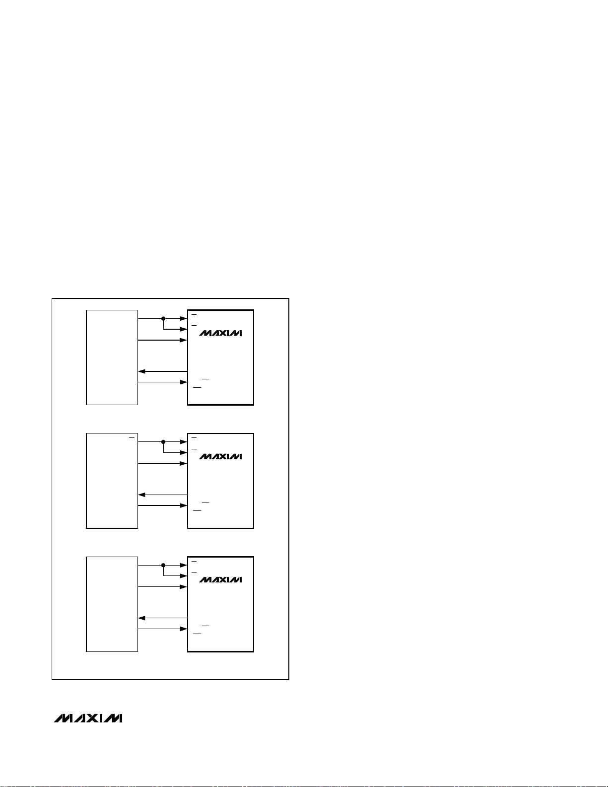
Serial Interface
The MAX1393/MAX1396 serial interface is fully compatible with SPI, QSPI, and MICROWIRE (see Figure 7). If a
serial interface is available, set the µC’s serial interface
in master mode so the µC generates the serial clock.
Choose a clock frequency between 100kHz and 5MHz.
CS and OE can be connected together and driven
simultaneously. OE can also be connected to GND if the
DOUT bus is not shared and driven independently.
SPI and MICROWIRE
When using SPI or MICROWIRE, make the µC the bus
master and set CPOL = 0 and CPHA = 0 or CPOL = 1
and CPHA = 1. (These are the bits in the SPI or
MICROWIRE control register.) Two consecutive 1-byte
reads are required to get the entire 12-bit result from
the ADC. DOUT transitions on SCLK’s falling edge and
is clocked into the µC on the SCLK’s rising edge. See
Figure 7 for connections and Figures 8 and 9 for timing
diagrams. The conversion result contains 4 zeros, followed by the 12 data bits with the data in MSB-first format. When using CPOL = 0 and CPHA = 0 or CPOL = 1
and CPHA = 1, the MSB of the data is clocked into the
µC on the SCLK’s fifth rising edge. To be compatible
with SPI and MICROWIRE, connect CS and OE togeth-
er and drive simultaneously.
QSPI
Unlike SPI, which requires two 1-byte reads to acquire
the 12 bits of data from the ADC, QSPI allows the minimum number of clock cycles necessary to clock in the
data. However, the MAX1393/MAX1396 require 16
clock cycles from the µC to clock out the 12 bits of
data. See Figure 7 for connections and Figures 8 and 9
for timing diagrams. The conversion result contains 4
zeros, followed by the 12 data bits with the data in
MSB-first format. When using CPOL = 0 and CPHA = 0
or CPOL = 1 and CPHA = 1, the MSB of the data is
clocked into the µC on the SCLK’s fifth rising edge. To
be compatible with QSPI, connect CS and OE together
and drive simultaneously.
DSP Interface
Figure 10 shows the timing for DSP operation. Figure
11 shows the connections between the MAX1393/
MAX1396 and several common DSPs.
MAX1393/MAX1396
______________________________________________________________________________________ 11
1.5V to 3.6V, 312.5ksps, 1-Channel True-Differential/
2-Channel Single-Ended, 12-Bit, SAR ADCs
MAX1393
MAX1396
OE
a) SPI
I/O
SCK
CS
DOUTMISO
I/O
UNI/BIP
(CH1/CH2)*
SCLK
MAX1393
MAX1396
OECS
SCK
CS
DOUTMISO
I/O
UNI/BIP
(CH1/CH2)*
SCLK
MAX1393
MAX1396
OEI/O
SK
CS
DOUTSI
I/O
UNI/BIP
(CH1/CH2)*
SCLK
b) QSPI
c) MICROWIRE
*INDICATES THE MAX1396
Figure 7. Common Serial-Interface Connections to the
MAX1393/MAX1396

MAX1393/MAX1396
12 ______________________________________________________________________________________
1.5V to 3.6V, 312.5ksps, 1-Channel True-Differential/
2-Channel Single-Ended, 12-Bit, SAR ADCs
ADC
STATE
BIPOLAR (AIN1)*
UNI (AIN2)*
123456789101112 13 14 15 16 1
SCLK
HIGH-Z
HIGH-Z
DOUT
D11 D10 D9 D8 D7 D6 D5 D4 D3 D2 D1 D0
POWER-
DOWN
POWERDOWN
SAMPLING INSTANT
UNI/BIP
(CH1/CH2)*
CS = OE
POWER-UP
AND ACQUIRE
(t
ACQ
)
HOLD
AND CONVERT
(t
CONV
)
*INDICATES THE MAX1396
Figure 8. Serial-Interface Timing for SPI/QSPI (CPOL = CPHA = 1) and MICROWIRE (G6 = 0, G5 = 1)
ADC
STATE
BIPOLAR (AIN1)*
UNI (AIN2)*
123456789101112 13 14 15 16 1
SCLK
HIGH-Z
HIGH-Z
DOUT
D11 D10 D9 D8 D7 D6 D5 D4 D3 D2 D1 D0
POWER-
DOWN
POWERDOWN
SAMPLING INSTANT
UNI/BIP
(CH1/CH2)*
CS = OE
POWER-UP
AND ACQUIRE
(t
ACQ
)
HOLD
AND CONVERT
(t
CONV
)
*INDICATES THE MAX1396
Figure 9. Serial-Interface Timing for SPI/QSPI (CPOL = CPHA = 0) and MICROWIRE (G6 = 0, G5 = 0)

As shown in Figure 11, drive the MAX1393/MAX1396
chip-select input (CS) with the DSP’s frame-sync signal.
OE may be connected to GND or driven independently.
For continuous conversion operation, keep OE low and
make the CS falling edge coincident with the 16th
falling edge of the SCLK.
Unregulated Two-Cell or Single Lithium
LiMnO
2
Cell Operation
Low operating voltage (1.5V to 3.6V) and ultra-low-power
consumption make the MAX1393/MAX1396 ideal for low
cost, unregulated, battery-powered applications without
the need for a DC-DC converter. Power the MAX1393/
MAX1396 directly from two alkaline/NiMH/NiCd cells in
series or a single lithium coin cell as shown in the Typical
Operating Circuit.
Fresh alkaline cells have a voltage of approximately
1.5V per cell (3V with 2 cells in series) and approach
end of life at 0.8V (1.6V with 2 cells in series). A typical
2xAA alkaline discharge curve is shown in Figure 12a.
A typical CR2032 lithium (LiMnO2) coin cell discharge
curve is shown in Figure 12b.
Layout, Grounding, and Bypassing
For best performance, use PC boards. Board layout
must ensure that digital and analog signal lines are
separated from each other. Do not run analog and digital (especially clock) lines parallel to one another, or
digital lines underneath the ADC package.
Figure 13 shows the recommended system ground
connections. Establish a single-point analog ground
(star ground point) at the MAX1393/MAX1396s’ GND
pin or use the ground plane.
High-frequency noise in the power supply (V
DD
)
degrades the ADC’s performance. Bypass V
DD
to GND
with a 0.1µF capacitor as close to the device as possible. Minimize capacitor lead lengths for best supply
noise rejection. To reduce the effects of supply noise, a
10Ω resistor can be connected as a lowpass filter to
attenuate supply noise.
Exposed Pad
The MAX1393/MAX1396 TDFN package has an
exposed pad on the bottom of the package. This pad is
not internally connected. Connect the exposed pad to
the GND pin on the MAX1393/MAX1396 or leave floating for proper electrical performance.
Definitions
Integral Nonlinearity (INL)
INL is the deviation of the values on an actual transfer
function from a straight line. For the MAX1393/
MAX1396, this straight line is between the end points of
the transfer function once offset and gain errors have
been nullified. INL deviations are measured at every
step and the worst-case deviation is reported in the
Electrical Characteristics section.
MAX1393/MAX1396
______________________________________________________________________________________ 13
1.5V to 3.6V, 312.5ksps, 1-Channel True-Differential/
2-Channel Single-Ended, 12-Bit, SAR ADCs
ADC
STATE
BIPOLAR (AIN1)*
UNI (AIN2)*
116 2 3 4 5 6 7 8 9 10 11 12 13 14 15 16
FS
21
SCLK
DOUT
D11D0 D10 D9 D8 D7 D6 D5 D4 D3 D2 D1 D0
POWERDOWN
POWERDOWN
SAMPLING INSTANT
CS
OE
POWER-UP
AND ACQUIRE
(t
ACQ
)
HOLD
AND CONVERT
(t
CONV
)
UNI/BIP
(CH1/CH2)*
*INDICATES THE MAX1396
Figure 10. DSP Serial-Timing Diagram

MAX1393/MAX1396
Differential Nonlinearity (DNL)
DNL is the difference between an actual step width and
the ideal value of 1 LSB. A DNL error specification of
less than ±1 LSB guarantees no missing codes and a
monotonic transfer function. For the MAX1393/
MAX1396, DNL deviations are measured at every step
and the worst-case deviation is reported in the
Electrical Characteristics section.
Signal-to-Noise Plus Distortion (SINAD)
SINAD is computed by taking the ratio of the RMS signal to the RMS noise plus the RMS distortion. RMS
noise includes all spectral components to the Nyquist
frequency excluding the fundamental, the first five harmonics (HD2–HD5), and the DC offset. RMS distortion
includes the first five harmonics (HD2–HD5):
SINAD
SIGNAL
NOISE DISTORTION
RMS
RMS RMS
log
=×
+
20
22
14 ______________________________________________________________________________________
1.5V to 3.6V, 312.5ksps, 1-Channel True-Differential/
2-Channel Single-Ended, 12-Bit, SAR ADCs
MAX1393
MAX1396
OE
a) TMS320C541 CONNECTION DIAGRAM
I/O
FSX
FSR
CS
DOUTDR
I/O
UNI/BIP
(CH1/CH2)*
CLKX
CLKR
SCLK
MAX1393
MAX1396
OE
b) ADSP218x CONNECTION DIAGRAM
I/O
TFS
RFS
CS
DOUTDR
I/O
UNI/BIP
(CH1/CH2)*
SCLK
SCLK
MAX1393
MAX1396
OE
c) DSP563xx CONNECTION DIAGRAM
*INDICATES THE MAX1396
I/O
SC2
CS
DOUT
I/O
UNI/BIP
(CH1/CH2)*
SLK
SDR
SCLK
Figure 11. Common DSP Connections to the MAX1393/MAX1396
DAYS
VOLTAGE (V)
1.8
2.0
2.2
2.4
2.6
2.8
3.0
1.6
0 700600500400300200100
TA = +25°C
Figure 12a. Typical 2xAA Discharge Curve at 100ksps
DAYS
VOLTAGE (V)
40302010
1.8
2.0
2.2
2.4
2.6
2.8
3.0
1.6
050
TA = +25°C
Figure 12b. Typical CR2032 Discharge Curve at 100ksps

Signal-to-Noise Ratio (SNR)
SNR is a dynamic figure of merit that indicates the converter’s noise performance. For a waveform perfectly
reconstructed from digital samples, the theoretical
maximum SNR is the ratio of the full-scale analog input
(RMS value) to the RMS quantization error (residual
error). The ideal, theoretical minimum analog-to-digital
noise is caused by quantization error only and results
directly from the ADC’s resolution (N bits):
SNR
dB[max]
= 6.02dBx N + 1.76
dB
In reality, there are other noise sources such as thermal
noise, reference noise, and clock jitter that also
degrade SNR. SNR is computed by taking the ratio of
the RMS signal to the RMS noise. RMS noise includes
all spectral components to the Nyquist frequency
excluding the fundamental, the first five harmonics, and
the DC offset.
Total Harmonic Distortion (THD)
THD is a dynamic figure of merit that indicates how much
harmonic distortion the converter adds to the signal.
THD is the ratio of the RMS sum of the first five harmonics of the fundamental signal to the fundamental itself.
This is expressed as:
where V1is the fundamental amplitude, and V2through
V6are the amplitudes of the 2nd- through 6th-order
harmonics.
Spurious-Free Dynamic Range (SFDR)
SFDR is a dynamic figure of merit that indicates the
lowest usable input signal amplitude. SFDR is the ratio
of the RMS amplitude of the fundamental (maximum
signal component) to the RMS value of the next-largest
spurious component, excluding DC offset. SFDR is
specified in decibels relative to the carrier (dBc).
Intermodulation Distortion (IMD)
IMD is the ratio of the RMS sum of the intermodulation
products to the RMS sum of the two fundamental input
tones. This is expressed as:
The fundamental input tone amplitudes (V1and V2) are
at -6.5dBFS. Fourteen intermodulation products (VIM_)
are used in the MAX1393/MAX1396 IMD calculation.
The intermodulation products are the amplitudes of the
output spectrum at the following frequencies, where f
IN1
and f
IN2
are the fundamental input tone frequencies:
• 2nd-order intermodulation products:
f
IN1
+ f
IN2
, f
IN2
- f
IN1
• 3rd-order intermodulation products:
2 x f
IN1
- f
IN2
, 2 x f
IN2
- f
IN1
, 2 x f
IN1
+ f
IN2
, 2 x f
IN2
+ f
IN1
• 4th-order intermodulation products:
3 x f
IN1
- f
IN2
, 3 x f
IN2
- f
IN1
, 3 x f
IN1
+ f
IN2
, 3 x f
IN2
+ f
IN1
• 5th-order intermodulation products:
3 x f
IN1
- 2 x f
IN2
, 3 x f
IN2
- 2 x f
IN1
, 3 x f
IN1
+ 2 x
f
IN2
, 3 x f
IN2
+ 2 x f
IN1
Channel-to-Channel Crosstalk
Channel-to-channel crosstalk indicates how well each
analog input is isolated from the others. The channel-tochannel crosstalk for the MAX1396 is measured by
applying DC to channel 2 while an AC sine wave is
applied to channel 1. An FFT is taken for channel 1 and
channel 2 and the difference (in dB) is reported as the
channel-to-channel crosstalk.
Aperture Delay
The MAX1393/MAX1396 sample data on the falling
edge of its third SCLK cycle (Figure 14). In actuality,
there is a small delay between the falling edge of the
sampling clock and the actual sampling instant.
Aperture delay (tAD) is the time defined between the
IMD
VV V V
VV
IM IM IM IMN
log
.....
=×
++++
+
20
1
2
2
2
3
22
1
2
2
2
THD
VVVVV
V
log
=×
++++
20
2
2
3
2
4
2
5
2
6
2
1
MAX1393/MAX1396
______________________________________________________________________________________ 15
1.5V to 3.6V, 312.5ksps, 1-Channel True-Differential/
2-Channel Single-Ended, 12-Bit, SAR ADCs
10Ω
(OPTIONAL)
V
DD
V
DD
POWER SUPPLY
GND
DIGITAL
CIRCUITRY
GND
DGND
DATA
STAR
GROUND
POINT
DV
DD
V
DD
MAX1393/MAX1396
Figure 13. Power-Supply Grounding Connections

MAX1393/MAX1396
falling edge of the sampling clock and the instant when
an actual sample is taken.
Aperture Jitter
Aperture jitter (tAJ) is the sample-to-sample variation in
the aperture delay (Figure 14).
DC Power-Supply Rejection Ratio (PSRR)
DC PSRR is defined as the change in the positive fullscale transfer function point caused by a full range variation in the analog power-supply voltage (VDD).
Chip Information
TRANSISTOR COUNT: 9106
PROCESS: BiCMOS
16 ______________________________________________________________________________________
1.5V to 3.6V, 312.5ksps, 1-Channel True-Differential/
2-Channel Single-Ended, 12-Bit, SAR ADCs
t
AD
T/H
(INTERNAL
SIGNAL)
SCLK
t
AJ
TRACK HOLD
ANALOG
INPUT
SAMPLED
DATA
THIRD FALLING EDGE
Figure 14. T/H Aperture Timing
AIN+
(AIN1)*
DOUT
SCLK
AIN(AIN2)*
REF
DIFFERENTIAL
INPUT
VOLTAGE
2 x AA CELLS
CPU
+
-
V
DD
GND
REF
INPUT
VOLTAGE
0.1µF
0.1µF
CS
OE
UNI/BIP
(CH1/CH2)*
MISO
SCL
SS
MAX1393
MAX1396
*INDICATES THE MAX1396 ONLY.
Typical Operating Circuit

MAX1393/MAX1396
______________________________________________________________________________________ 17
1.5V to 3.6V, 312.5ksps, 1-Channel True-Differential/
2-Channel Single-Ended, 12-Bit, SAR ADCs
1
2
3
4
5
µMAX
10
9
8
7
6
SCLK
DOUT
CS
OEGND
AIN+
AIN-
V
DD
MAX1393
TOP VIEW
REF UNI/BIP
CS
OE
UNI/BIP
GND
REF
1
2
3
4
5
10
98
7
6
SCLK
DOUT
AIN-
AIN+
V
DD
3mm x 3mm TDFN
TOP VIEW
MAX1393
1
2
3
4
5
µMAX
10
9
8
7
6
SCLK
DOUT
CS
OEGND
AIN1
AIN2
V
DD
MAX1396
TOP VIEW
REF CH1/CH2
TOP VIEW
CS
OE
CH1/CH2
GND
REF
1
2
3
4
5
10
98
7
6
SCLK
DOUT
AIN2
AIN1
V
DD
3mm x 3mm TDFN
MAX1396
Pin Configurations

Package Information
(The package drawing(s) in this data sheet may not reflect the most current specifications. For the latest package outline information,
go to www.maxim-ic.com/packages
.)
MAX1393/MAX1396
18 ______________________________________________________________________________________
1.5V to 3.6V, 312.5ksps, 1-Channel True-Differential/
2-Channel Single-Ended, 12-Bit, SAR ADCs
6, 8, &10L, DFN THIN.EPS
L
C
L
C
PIN 1
INDEX
AREA
D
E
L
e
L
A
e
E2
N
G
1
2
21-0137
PACKAGE OUTLINE, 6,8,10 & 14L,
TDFN, EXPOSED PAD, 3x3x0.80 mm
-DRAWING NOT TO SCALE-
k
e
[(N/2)-1] x e
REF.
PIN 1 ID
0.35x0.35
DETAIL A
b
D2
A2
A1
COMMON DIMENSIONS
SYMBOL
MIN. MAX.
A
0.70 0.80
D 2.90 3.10
E
2.90 3.10
A1
0.00 0.05
L
0.20 0.40
PKG. CODE
N
D2 E2 e
JEDEC SPEC
b
[(N/2)-1] x e
PACKAGE VARIATIONS
0.25 MIN.k
A2 0.20 REF.
2.30±0.101.50±0.106T633-1 0.95 BSC MO229 / WEEA 1.90 REF0.40±0.05
1.95 REF0.30±0.05
0.65 BSC
2.30±0.108T833-1
2.00 REF0.25±0.05
0.50 BSC
2.30±0.1010T1033-1
2.40 REF0.20±0.05- - - -
0.40 BSC
1.70±0.10 2.30±0.1014T1433-1
1.50±0.10
1.50±0.10
MO229 / WEEC
MO229 / WEED-3
0.40 BSC
- - - - 0.20±0.05 2.40 REFT1433-2 14 2.30±0.101.70±0.10
T633-2 6 1.50±0.10 2.30±0.10 0.95 BSC
MO229 / WEEA
0.40±0.05 1.90 REF
T833-2 8 1.50±0.10 2.30±0.10
0.65 BSC MO229 / WEEC
0.30±0.05 1.95 REF
T833-3 8 1.50±0.10 2.30±0.10
0.65 BSC MO229 / WEEC
0.30±0.05 1.95 REF
-DRAWING NOT TO SCALE-
G
2
2
21-0137
PACKAGE OUTLINE, 6,8,10 & 14L,
TDFN, EXPOSED PAD, 3x3x0.80 mm
DOWNBONDS
ALLOWED
NO
NO
NO
NO
YES
NO
YES
NO

MAX1393/MAX1396
Maxim cannot assume responsibility for use of any circuitry other than circuitry entirely embodied in a Maxim product. No circuit patent licenses are
implied. Maxim reserves the right to change the circuitry and specifications without notice at any time.
Maxim Integrated Products, 120 San Gabriel Drive, Sunnyvale, CA 94086 408-737-7600 ____________________ 19
© 2005 Maxim Integrated Products Printed USA is a registered trademark of Maxim Integrated Products, Inc.
Package Information (continued)
(The package drawing(s) in this data sheet may not reflect the most current specifications. For the latest package outline information,
go to www.maxim-ic.com/packages
.)
1.5V to 3.6V, 312.5ksps, 1-Channel True-Differential/
2-Channel Single-Ended, 12-Bit, SAR ADCs
10LUMAX.EPS
PACKAGE OUTLINE, 10L uMAX/uSOP
1
1
21-0061
I
REV.DOCUMENT CONTROL NO.APPROVAL
PROPRIETARY INFORMATION
TITLE:
TOP VIEW
FRONT VIEW
1
0.498 REF
0.0196 REF
S
6°
SIDE VIEW
α
BOTTOM VIEW
0° 0° 6°
0.037 REF
0.0078
MAX
0.006
0.043
0.118
0.120
0.199
0.0275
0.118
0.0106
0.120
0.0197 BSC
INCHES
1
10
L1
0.0035
0.007
e
c
b
0.187
0.0157
0.114
H
L
E2
DIM
0.116
0.114
0.116
0.002
D2
E1
A1
D1
MIN
-A
0.940 REF
0.500 BSC
0.090
0.177
4.75
2.89
0.40
0.200
0.270
5.05
0.70
3.00
MILLIMETERS
0.05
2.89
2.95
2.95
-
MIN
3.00
3.05
0.15
3.05
MAX
1.10
10
0.6±0.1
0.6±0.1
Ø0.50±0.1
H
4X S
e
D2
D1
b
A2
A
E2
E1
L
L1
c
α
GAGE PLANE
A2 0.030 0.037 0.75 0.95
A1

Copyright © Each Manufacturing Company.
All Datasheets cannot be modified without permission.
This datasheet has been download from :
www.AllDataSheet.com
100% Free DataSheet Search Site.
Free Download.
No Register.
Fast Search System.
www.AllDataSheet.com
 Loading...