

For free samples & the latest literature: http://www.maxim-ic.com, or phone 1-800-998-8800.
For small orders, phone 1-800-835-8769.
General Description
The MAX1108/MAX1109 low-power, 8-bit, dual-channel,
analog-to-digital converters (ADCs) feature an internal
track/hold (T/H) voltage reference, clock, and serial interface. The MAX1108 is specified from +2.7V to +3.6V and
consumes only 105µA. The MAX1109 is specified from
+4.5V to +5.5V and consumes only 130µA. The analog
inputs are software configurable, allowing unipolar/bipolar
and single-ended/differential operation; battery monitoring capability is also included.
The full-scale analog input range is determined by the
internal reference of +2.048V (MAX1108) or +4.096V
(MAX1109), or by an externally applied reference ranging from 1V to VDD. The MAX1108/MAX1109 also feature
a software power-down mode that reduces power consumption to 0.5µA when the device is not in use. The
4-wire serial interface directly connects to SPI™, QSPI™,
and MICROWIRE™ devices without external logic.
Conversions up to 50ksps are performed using either the
internal clock or an external serial-interface clock.
The MAX1108 and MAX1109 are available in a 10-pin
µMAX package with a footprint that is just 20% of an
8-pin plastic DIP.
Applications
Portable Data Logging
Hand-Held Measurement Devices
Medical Instruments
System Diagnostics
Solar-Powered Remote Systems
4–20mA-Powered Remote Systems
Receive-Signal Strength Indicators
Features
♦ Single Supply: +2.7V to +3.6V (MAX1108)
+4.5V to +5.5V (MAX1109)
♦ Low Power: 105µA at +3V and 50ksps
0.5µA in Power-Down Mode
♦ Software-Configurable Unipolar or Bipolar Inputs
♦ Input Voltage Range: 0 to V
DD
♦ Internal Track/Hold
♦ Internal Reference: +2.048V (MAX1108)
+4.096V (MAX1109)
♦ Reference Input Range: 1V to V
DD
♦ SPI/QSPI/MICROWIRE-Compatible Serial Interface
♦ V
DD
Monitoring Mode
♦ Small 10-Pin µMAX Package
MAX1108/MAX1109
Single-Supply, Low-Power,
2-Channel, Serial 8-Bit ADCs
________________________________________________________________
Maxim Integrated Products
1
1
2
3
4
5
10
9
8
7
6
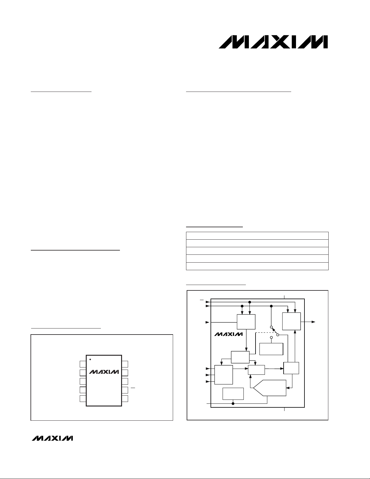
SCLK
DOUT
DIN
CSGND
CH1
CH0
V
DD
MAX1108
MAX1109
µMAX
TOP VIEW
COMREF
Functional Diagram
19-1399; Rev 0; 10/98
Pin Configuration
Ordering Information
PART
MAX1108CUB
MAX1108EUB -40°C to +85°C
0°C to +70°C
TEMP. RANGE PIN-PACKAGE
10 µMAX
10 µMAX
MAX1109CUB
MAX1109EUB -40°C to +85°C
0°C to +70°C 10 µMAX
10 µMAX
SPI and QSPI are trademarks of Motorola, Inc. MICROWIRE is a trademark of National Semiconductor Corp.
V
DD
CS
SCLK
OUTPUT
SHIFT
REGISTER
DIN
INPUT
SHIFT
REGISTER
DOUT
MAX1108
MAX1109
CONTROL
LOGIC
CH0
CH1
COM
REF
ANALOG
INPUT
MUX
REFERENCE
INTERNAL
INTERNAL
OSCILLATOR
T/H
CHARGE
REDISTRIBUTION
DAC
SAR
GND
MAX1108/MAX1109
Single-Supply, Low-Power,
2-Channel, Serial 8-Bit ADCs
2 _______________________________________________________________________________________
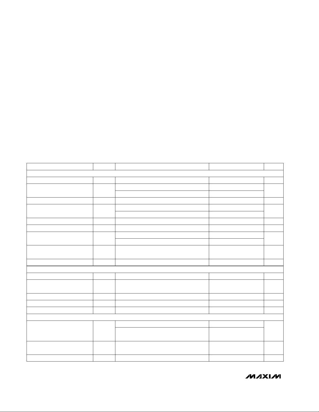
ABSOLUTE MAXIMUM RATINGS
ELECTRICAL CHARACTERISTICS—MAX1108
(VDD= +2.7V to +3.6V; unipolar input mode; COM = GND, f
SCLK
= 500kHz, external clock mode (50% duty cycle); 10 clocks/conver-
sion cycle (50ksps); 1µF capacitor at REF, external +2.048V reference at REF; T
A
= T
MIN
to T
MAX
; unless otherwise noted. Typical
values are at T
A
= +25°C.)
Stresses beyond those listed under “Absolute Maximum Ratings” may cause permanent damage to the device. These are stress ratings only, and functional
operation of the device at these or any other conditions beyond those indicated in the operational sections of the specifications is not implied. Exposure to
absolute maximum rating conditions for extended periods may affect device reliability.
VDDto GND..............................................................-0.3V to +6V
CH0, CH1, COM, REF, DOUT to GND.......-0.3V to (V
DD
+ 0.3V)
DIN, SCLK,
CS to GND ............................................-0.3V to +6V
Continuous Power Dissipation (T
A
= +70°C)
10-pin µMAX (derate 5.6mW/°C above +70°C)............444mW
Operating Temperature Ranges
MAX110_CUB......................................................0°C to +70°C
MAX110_EUB ...................................................-40°C to +85°C
Storage Temperature Range.............................-65°C to +150°C
Lead Temperature (soldering, 10sec).............................+300°C
V
DD
= 2.7V to 3.6V
VDD= 5.5V (Note 2)
No missing codes over temperature
CONDITIONS
±0.15 ±0.5
bits8Resolution
LSB
±0.2
INLRelative Accuracy (Note 1)
LSB±1DNLDifferential Nonlinearity
UNITSMIN TYP MAXSYMBOLPARAMETER
VDD= 5.5V (Note 2)
VDD= 2.7V to 3.6V
LSB
±0.5
Offset Error
±0.2 ±1
LSB±1Gain Error (Note 3)
ppm/°C±0.8Gain Temperature Coefficient
TA= T
MIN
to T
MAX
TA= +25°C
mV50V
DD
/ 2 Sampling Accuracy
dB49SINADSignal-to-Noise Plus Distortion
dB-70THD
Total Harmonic Distortion
(up to the 5th harmonic)
LSB
±0.5
TUETotal Unadjusted Error
±1
LSB±0.1
Channel-to-Channel
Offset Matching
-3dB rolloff
Unipolar input, V
COM
= 0
MHz0.8Full-Power Bandwidth
MHz1.5BW
-3dB
Small-Signal Bandwidth
0 V
REF
Input Voltage Range (Note 4)
dB68SFDRSpurious-Free Dynamic Range
Bipolar input, V
COM
or V
CH1
= V
REF
/ 2,
referenced to COM or CH1
V
±V
REF
/ 2
V
CH_
pF18C
IN
Input Capacitance
On/off-leakage current,
V
COM
or VCH= 0 or V
DD
µA±0.01 ±1Multiplexer Leakage Current
DC ACCURACY
DYNAMIC PERFORMANCE (10kHz sine-wave input, 2.048Vp-p, 50ksps, 500kHz external clock)
ANALOG INPUTS
µA
MAX1108/MAX1109
Single-Supply, Low-Power,
2-Channel, Serial 8-Bit ADCs
_______________________________________________________________________________________ 3
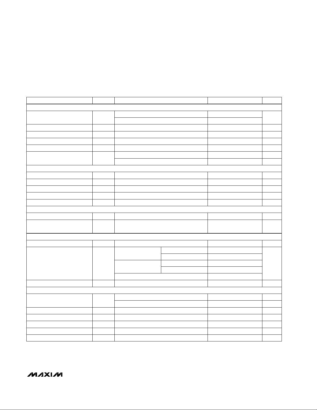
ELECTRICAL CHARACTERISTICS—MAX1108 (continued)
(VDD= +2.7V to +3.6V; unipolar input mode; COM = GND, f
SCLK
= 500kHz, external clock mode (50% duty cycle); 10 clocks/conver-
sion cycle (50ksps); 1µF capacitor at REF, external +2.048V reference at REF; T
A
= T
MIN
to T
MAX
; unless otherwise noted. Typical
values are at T
A
= +25°C.)
CONDITIONS UNITSMIN TYP MAXSYMBOLPARAMETER
External clock, 500kHz, 10 sclks/conv
Internal clock
External clock, 2MHz
µs
20
t
CONV
Conversion Time (Note 5)
35
µs1t
ACQ
Track/Hold Acquisition Time
ps<50Aperture Jitter
ns10Aperture Delay
kHz400Internal Clock Frequency
(Note 6)
0 to 0.5mA (Note 7)
ppm/°C±50REF Tempco
µA150I
REFSC
REF Short-Circuit Current
mV2.5Load Regulation
kHz50 500
V1.968 2.048 2.128V
REF
Output Voltage
+2.048V at REF, full scale,
500kHz external clock
µA1 20Input Current
V2.7 3 5.5V
DD
Supply Voltage
Power down, VDD= 2.7V to 3.6V
Full-scale input, VDD= 2.7V to 3.6V
0.5 2.5
I
DD
mV±0.4 ±4PSRPower-Supply Rejection (Note 9)
VDD= 2.7V to 3.6V,
C
L
= 10pF
VDD= 5.5V,
C
L
= 10pF
105 250
130
µF1Capacitive Bypass at REF
V0.2V
HYST
Input Hysteresis
V0.8V
IL
Threshold Voltage Low
µA±1I
IH
Input Current High
VDD≤ 3.6V
VDD> 3.6V
V2
V3
V
IH
Threshold Voltage High
MHz2
External Clock Frequency Range
V1.0 VDD+ 0.05Input Voltage Range
µA±1I
IL
Input Current Low
pF15C
IN
Input Capacitance
For data transfer only
Internal reference
External reference 70
Internal reference
External reference 95
µASupply Current (Notes 2, 8)
TRACK/HOLD
INTERNAL REFERENCE
EXTERNAL REFERENCE
POWER REQUIREMENTS
DIGITAL INPUTS (DIN, SCLK, and CS)
Wake-Up Time
MAX1108/MAX1109
Single-Supply, Low-Power,
2-Channel, Serial 8-Bit ADCs
4 _______________________________________________________________________________________
CS = V
DD
CS = V
DD
pF15C
OUT
Three-State Output Capacitance
µA±0.01 ±10I
L
Three-State Leakage Current
Figure 1, C
LOAD
= 100pF
Figure 1, C
LOAD
= 100pF
Figure 2, C
LOAD
= 100pF
ns240t
DV
CS Fall to Output Enable
ns
CONDITIONS
20 200t
DO
SCLK Fall to Output Data Valid
ns240t
TR
CS Rise to Output Disable
ns100t
DS
DIN to SCLK Setup Time
µs1.0t
ACQ
Acquisition Time
ns0t
DH
DIN to SCLK Hold Time
External reference
Internal reference (Note 10)
µs20
ns200t
CL
SCLK Pulse Width Low
ms12
t
WAKE
Wake-Up Time
ns0t
CSH
CS to SCLK Rise Hold
ns100t
CSS
CS to SCLK Rise Setup
ns200t
CH
SCLK Pulse Width High
UNITSMIN TYP MAXSYMBOLPARAMETER
I
SINK
= 5mA
I
SOURCE
= 0.5mA
I
SINK
= 16mA
V0.4
VVDD- 0.5V
OH
Output High Voltage
V0.8
V
OL
Output Low Voltage
ELECTRICAL CHARACTERISTICS—MAX1108 (continued)
(VDD= +2.7V to +3.6V; unipolar input mode; COM = GND, f
SCLK
= 500kHz, external clock mode (50% duty cycle); 10 clocks/conver-
sion cycle (50ksps); 1µF capacitor at REF, external +2.048V reference at REF; T
A
= T
MIN
to T
MAX
; unless otherwise noted. Typical
values are at T
A
= +25°C.)
ELECTRICAL CHARACTERISTICS—MAX1109
(VDD= +4.5V to +5.5V; unipolar input mode; COM = GND, f
SCLK
= 500kHz, external clock (50% duty cycle); 10 clocks/conversion
cycle (50ksps); 1µF capacitor at REF, external +4.096V reference at REF; T
A
= T
MIN
to T
MAX
; unless otherwise noted. Typical values
are at T
A
= +25°C.)
VDD= 4.5V to 5.5V LSBOffset Error ±0.2 ±1
LSB±1
VDD= 4.5V to 5.5V
No missing codes over temperature
Gain Error (Note 3)
ppm/°C±0.8
CONDITIONS
Gain Temperature Coefficient
TA= T
MIN
to T
MAX
TA= +25°C
mV50V
DD
/ 2 Sampling Accuracy
LSB
±0.5
TUETotal Unadjusted Error
±1
LSB±0.1
Channel-to-Channel
Offset Matching
±0.15 ±0.5
bits8Resolution
LSBINLRelative Accuracy (Note 1)
LSB±1DNLDifferential Nonlinearity
UNITSMIN TYP MAXSYMBOLPARAMETER
DIGITAL OUTPUT (DOUT)
TIMING CHARACTERISTICS (Figures 8, 9, and 10)
DC ACCURACY
MAX1108/MAX1109
Single-Supply, Low-Power,
2-Channel, Serial 8-Bit ADCs
_______________________________________________________________________________________ 5
ELECTRICAL CHARACTERISTICS—MAX1109 (continued)
(VDD= +4.5V to +5.5V; unipolar input mode; COM = GND, f
SCLK
= 500kHz, external clock (50% duty cycle); 10 clocks/conversion
cycle (50ksps); 1µF capacitor at REF, external +4.096V reference at REF; T
A
= T
MIN
to T
MAX
; unless otherwise noted. Typical values
are at T
A
= +25°C.)
ps<50Aperture Jitter
ns10Aperture Delay
kHz400Internal Clock Frequency
0 to 0.5mA (Note 7) ppm/°C±50REF Tempco
mA
CONDITIONS
5I
REFSC
REF Short-Circuit Current
mV2.5Load Regulation
kHz50 500
V
V3.936 4.096 4.256V
REF
Output Voltage
+4.096V at REF, full scale,
500kHz external clock
µA1 20Input Current
1.0 VDD+ 0.05Input Voltage Range
µF1Capacitive Bypass at REF
UNITSMIN TYP MAXSYMBOLPARAMETER
External clock, 2MHz
dBSINADSignal-to-Noise Plus Distortion 49
µs1t
ACQ
Track/Hold Acquisition Time
External clock, 500kHz, 10 sclks/conv
Internal clock
µs
20
t
CONV
Conversion Time (Note 5)
35
SFDRSpurious Free Dynamic Range dB
dB
68
THD
Total Harmonic Distortion
(up to the 5th harmonic)
-70
Full-Power Bandwidth MHz
Unipolar input, V
COM
= 0 0 V
REF
-3dB rolloff MHz
0.8
BW
-3dB
Small-Signal Bandwidth 1.5
V
CH_
Input Voltage Range (Note 4) V
Multiplexer Leakage Current µA
On/off-leakage current,
V
CH
= 0 or V
DD
±0.01 ±1
pFC
IN
Input Capacitance 18
Bipolar input, V
COM
or V
CH1
= V
REF
/ 2,
referenced to COM or CH1
±V
REF
/ 2
MHz2
External Clock Frequency Range
DYNAMIC PERFORMANCE (10kHz sine-wave input, 4.096Vp-p, 50ksps, 500kHz external clock)
ANALOG INPUTS
TRACK/HOLD
EXTERNAL REFERENCE
INTERNAL REFERENCE
For data transfer only
µA
MAX1108/MAX1109
Single-Supply, Low-Power,
2-Channel, Serial 8-Bit ADCs
6 _______________________________________________________________________________________
ELECTRICAL CHARACTERISTICS—MAX1109 (continued)
(VDD= +4.5V to +5.5V; unipolar input mode; COM = GND, f
SCLK
= 500kHz, external clock (50% duty cycle); 10 clocks/conversion
cycle (50ksps); 1µF capacitor at REF, external +4.096V reference at REF; T
A
= T
MIN
to T
MAX
; unless otherwise noted. Typical values
are at T
A
= +25°C.)
CS = V
DD
CS = V
DD
pF15C
OUT
Three-State Output Capacitance
µA±0.01 ±10I
L
Three-State Leakage Current
Figure 1, C
LOAD
= 100pF
Figure 1, C
LOAD
= 100pF
Figure 2, C
LOAD
= 100pF
ns240t
DV
CS Fall to Output Enable
ns
CONDITIONS
20 200t
DO
SCLK Fall to Output Data Valid
ns240t
TR
CS Rise to Output Disable
ns100t
DS
DIN to SCLK Setup Time
µs1.0t
ACQ
Acquisition Time
ns0t
DH
DIN to SCLK Hold Time
UNITSMIN TYP MAXSYMBOLPARAMETER
I
SINK
= 5mA
I
SINK
= 16mA
0.4
V4.5 5 5.5V
DD
Supply Voltage
V
0.8
V
OL
Output Low Voltage
VDD= 4.5V to 5.5V,
C
L
= 10pF,
full-scale input
130 250
Power down, VDD= 4.5V to 5.5V 0.5 2.5
95
External reference = +4.096V,
full-scale input, V
DD
= 4.5V to 5.5V
mV±0.4 ±4PSRPower-Supply Rejection (Note 9)
V0.2V
HYST
Input Hysteresis
V0.8V
IL
Threshold Voltage Low
V3V
IH
Threshold Voltage High
µA±1I
IH
Input Current High
pF15C
IN
Input Capacitance
I
SOURCE
= 0.5mA VVDD- 0.5V
OH
Output High Voltage
µA±1I
IL
Input Current Low
I
DD
µASupply Current (Notes 2, 8)
Internal reference
External reference
POWER REQUIREMENTS
DIGITAL INPUTS (DIN, SCLK, and CS)
DIGITAL OUTPUT (DOUT)
TIMING CHARACTERISTICS (Figures 8, 9, and 10)

MAX1108/MAX1109
Single-Supply, Low-Power,
2-Channel, Serial 8-Bit ADCs
_______________________________________________________________________________________ 7
ELECTRICAL CHARACTERISTICS—MAX1109 (continued)
(VDD= +4.5V to +5.5V; unipolar input mode; COM = GND, f
SCLK
= 500kHz, external clock (50% duty cycle); 10 clocks/conversion
cycle (50ksps); 1µF capacitor at REF, external +4.096V reference at REF; T
A
= T
MIN
to T
MAX
; unless otherwise noted. Typical values
are at T
A
= +25°C.)
CONDITIONS
External reference
Internal reference (Note 10)
µs20
ns200t
CL
SCLK Pulse Width Low
ms12
t
WAKE
Wake-Up Time
ns0t
CSH
CS to SCLK Rise Hold
ns100t
CSS
CS to SCLK Rise Setup
ns200t
CH
SCLK Pulse Width High
UNITSMIN TYP MAXSYMBOLPARAMETER
Note 1: Relative accuracy is the deviation of the analog value at any code from its theoretical value after the full-scale range has
been calibrated.
Note 2: See
Typical Operating Characteristics
.
Note 3: V
REF
= +2.048V (MAX1108), V
REF
= +4.096V (MAX1109), offset nulled.
Note 4: Common-mode range (CH0, CH1, COM) GND to V
DD
.
Note 5: Conversion time defined as the number of clock cycles times the clock period; clock has 50% duty cycle (Figures 6 and 8).
Note 6: REF supplies typically 2.5mA under normal operating conditions.
Note 7: External load should not change during the conversion for specified accuracy.
Note 8: Power consumption with CMOS levels.
Note 9: Measured as V
FS
(2.7V) - VFS(3.6V) for MAX1108, and measured as VFS(4.5V) - VFS(5.5V) for MAX1109.
Note 10: 1µF at REF, internal reference settling to 0.5LSB.
Typical Operating Characteristics
(VDD= +3.0V (MAX1108), VDD= +5.0V (MAX1109); external conversion mode; f
SCLK
= 500kHz; 50ksps; external reference; 1µF at
REF; TA= +25°C; unless otherwise noted.)
200
0
0 6
SUPPLY CURRENT vs. SUPPLY VOLTAGE
40
20
180
160
MAX1108/09-01
SUPPLY VOLTAGE (V)
SUPPLY CURRENT (µA)
1 2 3 4 5
140
120
100
80
60
D
OUT
= 10101010
MAX1108 (2.7V TO 5.5V)
MAX1109 (4.5V TO 5.5V)
INTERNAL REFERENCE
C
LOAD
= 47pF
C
LOAD
= 10pF
200
0
-40 100
SUPPLY CURRENT vs. TEMPERATURE
40
20
180
160
MAX1108/09-02
TEMPERATURE (°C)
SUPPLY CURRENT (µA)
-20 0 20 40 60 80
140
120
100
80
60
VDD = 5V
VDD = 3V
D
OUT
= 10101010
C
LOAD
= 10pF
INTERNAL REFERENCE
0.50
0
2.5 5.5
SHUTDOWN SUPPLY CURRENT
vs. SUPPLY VOLTAGE
0.10
0.05
0.45
0.40
MAX1108/09-03
SUPPLY VOLTAGE (V)
SHUTDOWN CURRENT (µA)
3.0 3.5 4.0 4.5 5.0
0.35
0.30
0.25
0.20
0.15

MAX1108/MAX1109
Single-Supply, Low-Power,
2-Channel, Serial 8-Bit ADCs
8 _______________________________________________________________________________________
Typical Operating Characteristics (continued)
(VDD= +3.0V (MAX1108), VDD= +5.0V (MAX1109); external conversion mode; f
SCLK
= 500kHz; 50ksps; external reference; 1µF at
REF; TA= +25°C; unless otherwise noted.)
0.5
-0.5
2.5 5.5
OFFSET ERROR vs. SUPPLY VOLTAGE
-0.3
-0.4
0.4
0.3
MAX1108/09-04
SUPPLY VOLTAGE (V)
OFFSET ERROR (LSB)
3.0 3.5 4.0 4.5 5.0
0.2
0.1
0
-0.1
-0.2
0.5
-0.5
-40 100
OFFSET ERROR vs. TEMPERATURE
-0.3
-0.4
0.4
0.3
MAX1108/09-05
TEMPERATURE (°C)
OFFSET ERROR (LSB)
-20 0 20 40 60 80
0.2
0.1
0
-0.1
-0.2
0.20
-0.20
0 5.0
OFFSET ERROR vs. REFERENCE VOLTAGE
-0.10
-0.15
0.15
0.10
MAX1108/09-06
REFERENCE VOLTAGE (V)
OFFSET ERROR (LSB)
0.5 1.0 1.5 2.0 2.5 3.0 3.5 4.0 4.5
0.05
0
-0.05
0.5
-0.5
2.5 5.5
GAIN ERROR vs. SUPPLY VOLTAGE
-0.3
-0.4
0.4
0.3
MAX1108/09-07
SUPPLY VOLTAGE (V)
GAIN ERROR (LSB)
3.0 3.5 4.0 4.5 5.0
0.2
0.1
0
-0.1
-0.2
0.3
-0.3
2.5 5.5
INTEGRAL NONLINEARITY
vs. SUPPLY VOLTAGE
-0.1
-0.2
0.2
MAX1108/09-10
SUPPLY VOLTAGE (V)
INL (LSB)
3.0 3.5 4.0 4.5 5.0
0.1
0
1.0
-1.0
-40 100
GAIN ERROR vs. TEMPERATURE
-0.6
-0.8
0.8
0.6
MAX1108/09-08
TEMPERATURE (°C)
GAIN ERROR (LSB)
-20 0 20 40 60 80
0.4
0.2
0
-0.2
-0.4
1.0
-1.0
0 5.0
GAIN ERROR vs. REFERENCE VOLTAGE
-0.4
-0.6
-0.8
0.8
0.6
MAX1108/09-09
REFERENCE VOLTAGE (V)
GAIN ERROR (LSB)
0.5 1.0 1.5 2.0 2.5 3.0 3.5 4.0 4.5
0.4
0
0.2
-0.2
0.5
-0.5
0 300
DIFFERENTIAL NONLINEARITY
vs. CODE
-0.1
0
-0.3
-0.4
-0.2
0.4
0.3
MAX1108/09-11
DIGITAL CODE
DNL (LSB)
50 100 150 200 250
0.1
0.2
0.5
-0.5
2.5 5.5
DIFFERENTIAL NONLINEARITY
vs. SUPPLY VOLTAGE
-0.2
-0.3
-0.4
0.4
0.3
MAX1108/09-12
SUPPLY VOLTAGE (V)
DNL (LSB)
3.0 3.5 4.0 4.5 5.0
0.2
0.1
0
-0.1

MAX1108/MAX1109
Single-Supply, Low-Power,
2-Channel, Serial 8-Bit ADCs
_______________________________________________________________________________________
9
0.5
-0.5
0 300
INTEGRAL NONLINEARITY
vs. CODE
-0.1
0
-0.3
-0.4
-0.2
0.4
0.3
MAX1108/09-13
DIGITAL CODE
INL (LSB)
50 100 150 200 250
0.1
0.2
20
-100
0 30
FFT PLOT
-60
-80
0
MAX1108/09-14
FREQUENCY (kHz)
AMPLITUDE (dB)
5 10 15 20 25
-20
-40
f
CH_
= 9997Hz, 2Vp-p
f
SAMPLE
= 53.25kHz
21.0
18.0
0 6
CONVERSION TIME vs. SUPPLY VOLTAGE
19.0
18.5
20.5
MAX1108/09-15
SUPPLY VOLTAGE (V)
CONVERSION TIME(µs)
1 2 3 4 5
20.0
19.5
INTERNAL CONVERSION MODE
Typical Operating Characteristics (continued)
(VDD= +3.0V (MAX1108), VDD= +5.0V (MAX1109); external conversion mode; f
SCLK
= 500kHz; 50ksps; external reference; 1µF at
REF; TA= +25°C; unless otherwise noted.)
Pin Description
Sampling Analog InputsCH0, CH12, 3
Reference voltage for analog-to-digital conversion (internal or external reference). Reference input for
external reference. Bypass internal reference with 1µF capacitor to GND.
REF5
GroundGND4
Active-Low Chip Select. Data is not clocked into DIN unless CS is low. When CS is high, DOUT is high
impedance.
CS
7
Serial Data Output. Data is clocked out on the falling edge of SCLK. High impedance when CS is high.
DOUT9
Serial Data Input. Data is clocked in at the rising edge of SCLK.DIN8
Common reference for analog inputs. Sets zero-code voltage in single-ended mode. Must be stable to
±0.5LSB during conversion.
COM6
Serial Clock Input. Clocks data in and out of serial interface. In external clock mode, SCLK also sets the
conversion speed.
SCLK10
PIN
Positive Supply VoltageV
DD
1
FUNCTIONNAME
CONVERSION TIME vs. TEMPERATURE
25
24
INTERNAL CONVERSION MODE
23
22
21
20
19
18
CONVERSION TIME (µs)
17
16
15
-40 100
-20 0 20 40 60 80
VDD = 3V
VDD = 5V
TEMPERATURE (°C)
MAX1108/09-16
REFERENCE VOLTAGE (V)
NORMALIZED REFERENCE VOLTAGE
vs. TEMPERATURE
1.0010
1.0005
1.0000
0.9995
0.9990
0.9985
0.9980
-40 100
-20 0 20 40 60 80
TEMPERATURE (°C)
CHANNEL-TO-CHANNEL
CROSSTALK vs. FREQUENCY
0
V
= V
CH_OFF
REFp-p
0 25
5 10 15 20
FREQUENCY (kHz)
MAX1108/09-17
CROSSTALK (dB)
-10
-20
-30
-40
-50
-60
-70
-80
-90
-100
MAX1108/09-18

MAX1108/MAX1109
Single-Supply, Low-Power,
2-Channel, Serial 8-Bit ADCs
10 ______________________________________________________________________________________
_______________Detailed Description
The MAX1108/MAX1109 analog-to-digital converters
(ADCs) use a successive-approximation conversion
technique and input track/hold (T/H) circuitry to convert
an analog signal to an 8-bit digital output. A flexible
serial interface provides easy interface to microprocessors (µPs). No external hold capacitors are required. All
of the MAX1108/MAX1109 operating modes are software-configurable: internal or external reference, internal or external conversion clock, single-ended unipolar
or pseudo-differential unipolar/bipolar conversion, and
power down (Table 1).
Analog Inputs
Track/Hold
The input architecture of the ADCs is illustrated in the
equivalent-input circuit of Figure 4 and is composed of
the T/H, the input multiplexer, the input comparator, the
switched capacitor DAC, the reference, and the autozero rail.
The analog-inputs configuration is determined by the
control-byte through the serial interface as shown in
Table 2 (see
Modes of Operation
section and Table 1).
The eight modes of operation include single-ended,
pseudo-differential, unipolar/bipolar, and a VDDmonitoring mode. During acquisition and conversion, only
one of the switches in Figure 4 is closed at any time.
The T/H enters its tracking mode on the falling clock
edge after bit 4 (SEL0) of the control byte has been
shifted in. It enters its hold mode on the falling edge
after the bit 2 (I/EREF) of the control byte has been
shifted in.
For example, If CH0 and COM are chosen (SEL2 =
SEL1 = SEL0 = 1) for conversion, CH0 is defined as the
sampled input (SI), and COM is defined as the reference input (RI). During acquisition mode, the CH0
switch and the T/H switch are closed, charging the
VDD
3k
C
LOAD
DGND
DOUT
C
LOAD
DGND
3k
DOUT
a) High-Z to V
OH
and VOL to V
OH
b) High-Z to VOL and VOH to V
OL
Figure 1. Load Circuits for Enable Time
V
DD
3k
C
LOAD
DGND
DOUT
C
LOAD
DGND
3k
DOUT
a) V
OH
to High-Z b) VOL to High-Z
Figure 2. Load Circuits for Disable Time
V
DD
I/O
SCK (SK)
MOSI (SO)
MISO (SI)
V
SS
DOUT
DIN
SCLK
CS
COM
GND
V
DD
CH1
1µF
0.1µF
1µF
CH0
ANALOG
INPUTS
MAX1108
MAX1109
CPU
V
DD
REF
Figure 3. Typical Operating Circuit
CH0
COM
V
DD
/ 2
GND
CH1
REF
GND
C
HOLD
CAPACITIVE DAC
COMPARATOR
18pF
R
IN
6.5k
AUTOZERO
RAIL
TRACK
HOLD
Figure 4. Equivalent Input Circuit

MAX1108/MAX1109
Single-Supply, Low-Power,
2-Channel, Serial 8-Bit ADCs
______________________________________________________________________________________ 11
holding capacitor C
HOLD
through RIN. At the end of
acquisition the T/H switch opens and C
HOLD
is con-
nected to COM, retaining charge on C
HOLD
as a sample of the signal at CH0, and the difference between
CH0 and COM is the converted signal. Once conversion is complete, the T/H returns immediately to its
tracking mode. This procedure holds for the different
combinations summarized in Table 2.
The time available for the T/H to acquire an input signal
(t
ACQ
) is determined by the clock frequency, and is 1µs
at the maximum clock frequency of 2MHz. The acquisition time is also the minimum time needed for the signal
to be acquired. It is calculated by:
t
ACQ
= 6(RS+ RIN)18pF
where RIN= 6.5kΩ, RS= the source impedance of
the input signal, and t
ACQ
is never less than 1µs.
Note that source impedances below 2.7kΩ do not
significantly affect the AC performance of the ADC at
the maximum clock speed. If the input-source impedance is higher than 3kΩ, the clock speed must be
reduced accordingly.
Pseudo-Differential Input
The MAX1108/MAX1109 input configuration is pseudodifferential to the extent that only the signal at the sampled input (SI) is stored in the holding capacitor
(C
HOLD
). The reference input (RI) must remain stable
within ±0.5LSB (±0.1LSB for best results) in relation to
GND during a conversion. Sampled input and reference input configuration is determined by bit6–bit4
(SEL2–SEL0) of the control byte (Table 2).
If a varying signal is applied at the selected reference
input, its amplitude and frequency need to be limited.
The following equations determine the relationship
between the maximum signal amplitude and its frequency to maintain ±0.5LSB accuracy:
Assuming a sinusoidal signal at the reference input
the maximum voltage variation is determined by:
a 60Hz signal at RI with an amplitude of 1.2V will generate a ±0.5LSB of error. This is with a 35µs conversion
time (maximum t
CONV
in internal conversion mode) and
a reference voltage of +4.096V. When a DC reference
voltage is used at RI, connect a 0.1µF capacitor to
GND to minimize noise at the input.
The input configuration selection also determines
unipolar or bipolar conversion mode. The commonmode input range of CH0, CH1, and COM is 0 to +V
DD
.
In unipolar mode, full scale is achieved when (SI - RI) =
V
REF
; in bipolar mode, full scale is achieved when (SI
- RI)= V
REF
/ 2. In unipolar mode, SI must be higher
than RI; in bipolar mode, SI can span above and below
RI provided that it is within the common-mode range.
Conversion Process
The comparator negative input is connected to the autozero rail. Since the device requires only a single supply,
the ZERO node at the input of the comparator equals
VDD/2. The capacitive DAC restores node ZERO to have
0V difference at the comparator inputs within the limits
of 8-bit resolution. This action is equivalent to transferring a charge of 18pF(V
IN+
- V
IN-
) from C
HOLD
to the
binary-weighted capacitive DAC which, in turn, forms a
digital representation of the analog-input signal.
Input Voltage Range
Internal protection diodes that clamp the analog input
to VDDand AGND allow the channel input pins (CH0,
CH1, and COM) to swing from (AGND - 0.3V) to (VDD+
0.3V) without damage. However, for accurate conversions, the inputs must not exceed (VDD+ 50mV) or be
less than (GND - 50mV).
If the analog input voltage on an “off” channel
exceeds 50mV beyond the supplies, the current
should be limited to 2mA to maintain conversion
accuracy on the “on” channel.
The MAX1108/MAX1109 input range is from 0 to VDD;
unipolar or bipolar conversion is available. In unipolar
mode, the output code is invalid (code zero) when a
negative input voltage (or a negative differential input
voltage) is applied. The reference input-voltage range
at REF is from 1V to (V
DD
+ 50mV.)
Input Bandwidth
The ADC’s input tracking circuitry has a 1.5MHz smallsignal bandwidth, so it is possible to digitize highspeed transient events and measure periodic signals
with bandwidths exceeding the ADC’s sampling rate by
using undersampling techniques. To avoid high-frequency signals being aliased into the frequency band
of interest, anti-alias filtering is recommended.
Serial Interface
The MAX1108/MAX1109 have a 4-wire serial interface.
The CS, DIN, and SCLK inputs are used to control the
device, while the three-state DOUT pin is used to
access the result of conversion.
max
dv
dt
2 f v
1 LSB
t
V
2 t
RI
RI
CONV
REF
8
= ≤ =⋅π
v V sin(2 ft)
RI RI
= π

MAX1108/MAX1109
Single-Supply, Low-Power,
2-Channel, Serial 8-Bit ADCs
12 ______________________________________________________________________________________
The serial interface provides easy connection to microcontrollers with SPI, QSPI and MICROWIRE serial interfaces at clock rates up to 2MHz. For SPI and QSPI, set
CPOL = CPHA = 0 in the SPI control registers of the
microcontroller. Figure 5 shows the MAX1108/MAX1109
common serial-interface connections.
Digital Inputs
The logic levels of the MAX1108/MAX1109 digital input
are set to accept voltage levels from both +3V and +5V
systems, regardless of the supply voltages. Input data
(control byte) is clocked in at the DIN pin on the rising
edge of serial clock (SCLK). CS is the standard chipselect signal which enables communication with the
device. SCLK is used to clock data in and out of serial
interface. In external clock mode, SCLK also sets the
conversion speed.
Digital Output
Output data is read on the rising edge of SCLK at
DOUT, MSB first (D7). In unipolar input mode, the output is straight binary. For bipolar input mode, the output
is twos-complement (see
Transfer Function
section).
DOUT is active when CS is low and high impedance
when CS is high. DOUT does not accept external voltages greater than V
DD
. In external-clock mode, data is
clocked out at the maximum clock rate of 500kHz while
conversion is in progress. In internal-clock mode, data
can be clocked out at up to 2MHz clock rate.
Modes of Operation
The MAX1108/MAX1109 feature single-ended or pseudo-differential operation in unipolar or bipolar configuration. The device is programmed through the input
control-byte at the DIN pin of the serial interface
(Table 1). Table 2 shows the analog-input configuration
and Table 3 shows the input-voltage ranges in unipolar
and bipolar configuration.
How to Start a Conversion
A conversion is started by clocking a control byte into
DIN. With CS low, each rising edge on SCLK clocks a
bit from DIN into the MAX1108/MAX1109’s internal shift
register. After CS falls, the first arriving logic “1” bit at
DIN defines the MSB of the control byte. Until this first
start bit arrives, any number of logic “0” bits can be
clocked into DIN with no effect. Table 1 shows the control-byte format.
Using the
Typical Operating Circuit
(Figure 3), the simplest software interface requires two 8-bit transfers to
perform a conversion (one 8-bit transfer to configure
the ADC, and one 8-bit transfer to clock out the 8-bit
conversion result). Figure 6 shows a single-conversion
timing diagram using external clock mode.
Clock Modes
The MAX1108/MAX1109 can use either an external serial clock or the internal clock to perform the successiveapproximation conversion. In both clock modes, the
external clock shifts data in and out of the devices. Bit
3 of control-byte (I/ECLK) programs the clock mode.
Figure 8 shows the timing characteristics common to
both modes.
External Clock
In external clock mode, the external clock not only
shifts data in and out, it also drives the analog-to-digital
conversion steps. In this mode the clock frequency
must be between 50kHz and 500kHz. Single-conversion timing using an external clock begins with a falling
edge on CS. When this occurs, DOUT leaves the high
impedance state and goes low. The first “1” clocked
into DIN by SCLK after CS is set low is considered as
the start bit. The next seven clocks latch in the rest of
the control byte. On the falling edge of the fourth clock,
track mode is enabled, and on the falling edge of the
sixth clock, acquisition is complete and conversion is
CS
SCLK
DOUT
I/O
SCK
MISO
+3V
SS
a) SPI
CS
SCLK
DOUT
CS
SCK
MISO
+3V
SS
b) QSPI
MAX1108
MAX1109
MAX1108
MAX1109
MAX1108
MAX1109
CS
SCLK
DOUT
I/O
SK
DINMOSI
DINMOSI
DINSO
SI
c) MICROWIRE
Figure 5. Common Serial-Interface Connections

MAX1108/MAX1109
Single-Supply, Low-Power,
2-Channel, Serial 8-Bit ADCs
______________________________________________________________________________________ 13
Table 1. Control Byte Format
Table 2. Conversion Configuration
Table 3. Full- and Zero-Scale Voltages
*
RI = Reference Input (Table 2)
START SEL2 SEL1 SEL0 I/ECLK I/EREF REFSHDN SHDN
BIT 7 BIT 6 BIT 5 BIT 4 BIT 3 BIT 2 BIT 1 BIT 0
(MSB) (LSB)
NAME
I/EREF2
BIT
1 = internal reference, 0 = external reference. Internal reference selects +2.048V (MAX1108) or
+4.096V (MAX1109), or an external reference can be applied to the REF pin.
DESCRIPTION
I/ECLK3
START
1 = external clock, 0 = internal clock. The SAR can be driven by the internal oscillator, or with the
SCLK signal.
SHDN
0 (LSB)
7 (MSB)
1 = operational, 0 = power down. For a full power down set REFSHDN = SHDN = 0. (See
Power-
Down Mode
section.)
The first logic “1” bit after CS goes low defines the beginning of the control byte.
SEL2
SEL1
SEL0
6
5
4
Selects the mode of operation (Table 2).
REFSHDN
1
1 = operational (if I / EREF = 1), 0 = reference shutdown. When using an external reference, power
consumption can be minimized by powering down the internal reference separately (I / EREF = 0).
REFSHDN must be set to 0 when SHDN = 0.
UNIPOLAR MODE
RI* RI - V
REF
/ 2
Zero Scale
RI + V
REF
RI RI + V
REF
/ 2
Negative
Full Scale
Full Scale
Zero
Scale
BIPOLAR MODE
Positive
Full Scale
SEL2
1
1
1
1
SEL1
SAMPLED INPUT
(SI)
SEL0
0
1
CH1
CH0
CONVERSION MODE
REFERENCE INPUT
(RI)
COM
COM
Unipolar
Unipolar
1 0
1
0
1
CH1
CH00
GND
GND
Unipolar
Unipolar
0 0
0
1
1
CH1
CH01
COM
COM
Bipolar
Bipolar
0 0
0
0
1
VDD/ 2
CH00
GND
CH1
Unipolar
Bipolar

MAX1108/MAX1109
Single-Supply, Low-Power,
2-Channel, Serial 8-Bit ADCs
14 ______________________________________________________________________________________
initiated. The MSB successive-approximation bit decision is made on the rising edge of the seventh SCLK.
On the falling edge of the eighth SCLK, the MSB is
clocked out on the DOUT pin; on each of the next
seven SCLK falling edges, the remaining bits of conversion are clocked out. Zeros are clocked out on DOUT
after the LSB has been clocked out, until CS is disabled. Then DOUT becomes high impedance and the
part is ready for another conversion (Figure 6).
The conversion must complete in 1ms, or droop on the
sample-and-hold capacitors may degrade conversion
results. Use internal clock mode if the serial-clock frequency is less than 50kHz, or if serial-clock interruptions could cause the conversion interval to exceed
1ms.
Internal Clock
Internal clock mode frees the µP from the burden of
running the SAR conversion clock. This allows the conversion results to be read back at the processor’s convenience, at any clock rate up to 2MHz.
An internal register stores data when the conversion is
in progress. On the falling edge of the fourth SCLK,
track mode is enabled, and on the falling edge of the
eighth SCLK, acquisition is complete and internal conversion is initiated. The internal 400kHz clock completes the conversion in 20µs typically (35µs max), at
which time the MSB of the conversion is present at the
DOUT pin. The falling edge of SCLK clocks the remaining data out of this register at any time after the conversion is complete (Figure 8).
CS
SCLK
DIN
DOUT
1 4 8 12 16 20
START
SEL2
MSB LSB
SEL1 SEL0 I/ECLK I/EREF
REF
SHDN
SHDN
D7
MSB
LSB
D6 D5 D4 D3 D2 D1 D0
IDLE
IDLE
t
CONV
t
ACQ
A/D STATE
Figure 6. Single Conversion Timing, External Clock Mode
• • •
• • •
• • •
• • •
CS
SCLK
DIN
DOUT
t
CSH
t
CSS
t
CL
t
DS
t
DH
t
DV
t
CH
t
DO
t
TR
t
CSH
Figure 7. Detailed Serial-Interface Timing

MAX1108/MAX1109
Single-Supply, Low-Power,
2-Channel, Serial 8-Bit ADCs
______________________________________________________________________________________ 15
CS does not need to be held low once a conversion is
started. Pulling CS high prevents data from being
clocked into the MAX1108/MAX1109 and three-states
DOUT, but it does not adversely affect an internal
clock-mode conversion already in progress. In this
mode, data can be shifted in and out of the
MAX1108/MAX1109 at clock rates up to 2MHz, provided that the minimum acquisition time (t
ACQ
) is kept
above 1µs.
Quick Look
To quickly evaluate the MAX1108/MAX1109’s analog
performance, use the circuit of Figure 9. The device
requires a control byte to be written to DIN before each
conversion. Tying CS to GND and DIN to VDDfeeds in
control bytes of FFH. In turn, this triggers single-ended,
unipolar conversions on CH0 in relation to COM in
external clock mode without powering down between
conversions. Apply an external 50kHz to 500kHz clock
CS
SCLK
DIN
DOUT
1 4 8
START
SEL2 SEL1SEL0
I/EREF I/ECLK
REF
SHDN
SHDN
D7 D6 D5
D4
D3 D2 D1 D0
t
ACQ
IDLE
IDLE
A/D STATE
10 14 18
t
CONV
35µs MAX
Figure 8. Single Conversion Timing, Internal Clock Mode
1µF
0.1µF
V
DD
GND
CS
SCLK
DIN
DOUT
V
DD
0.01µF
CH0
COM
REF
C1
1µF
ANALOG
INPUT
OSCILLOSCOPE
CH1
CH2
5µs/div
*CONVERSION RESULT = 10101010
MAX1108
MAX1109
V
SUPPLY
500kHz
OSCILLATOR
DOUT*
SCLK
MSB
LSB
Figure 9. Quick-Look Schematic

MAX1108/MAX1109
Single-Supply, Low-Power,
2-Channel, Serial 8-Bit ADCs
16 ______________________________________________________________________________________
to the SCLK pin; varying the analog input alters the
result of conversion that is clocked out at the DOUT pin.
A total of 10 clock cycles is required per conversion.
Data Framing
The falling edge of CS does not start a conversion. The
first logic high clocked into DIN is interpreted as a start
bit and defines the first bit of the control byte.
Acquisition starts on the falling edge of the fourth SCLK
and lasts for two SCLKs in external clock mode or four
SCLKs in internal clock mode. Conversion starts immediately after acquisition is completed. The start bit is
defined as:
The first high bit clocked into DIN with CS
low any time the converter is idle; e.g., after
VDDis applied.
OR
In external clock mode, the first high bit
clocked into DIN after the bit 5 (D5) of a conversion in progress is clocked onto the
DOUT pin.
OR
In internal clock mode, the first high bit
clocked into DIN after the bit 4 (D4) is
clocked onto the DOUT pin.
The MAX1108/MAX1109 can run at a maximum speed
of 10 clocks per conversion. Figure 10 shows the serialinterface timing necessary to perform a conversion
every 10 SCLK cycles in external clock mode.
Many microcontrollers require that conversions occur in
multiples of 8 SCLK clocks; 16 clocks per conversion is
typically the fastest that a microcontroller can drive the
MAX1108/MAX1109. Figure 11 shows the serial-interface timing necessary to perform a conversion every 16
SCLK cycles in external clock mode.
SCLK
DIN
DOUT
CS
S CONTROL BYTE 0
CONTROL BYTE 1S
CONVERSION RESULT 0
D7 D5 D0 D7 D5 D0
D7
CONVERSION RESULT 1
CONTROL BYTE 2S
1
8 10 1 10
1
10 1
S
t
ACQ
t
ACQ
t
ACQ
IDLE
A/D STATE
t
CONV
t
CONV
t
CONV
Figure 10. Continuous Conversion, External Clock Mode, 10 Clocks/Conversion Timing
SCLK
DIN
DOUT
CS
S CONTROL BYTE 0
CONTROL BYTE 1S
CONVERSION RESULT 0
D7 D0 D7 D0
CONVERSION RESULT 1
S
1
8 17
25
Figure 11. Continuous Conversion, External Clock Mode, 16 Clocks/Conversion Timing

In external clock mode, if CS is toggled before the current conversion is complete, the current conversion is
terminated, and the next high bit clocked into DIN is
recognized as a new start bit. This can be useful in
extending acquisition time by selecting conversion on
the same channel with the second control byte (doubleclocking mode), effectively extending acquisition to 6
SCLKs. This technique is ideal if the analog input
source has high impedance, or if it requires more than
1µs to settle; it can also be used to allow the device
and the reference to settle when using power downmodes (see
Power-Down Modes
section).
__________Applications Information
Battery Monitoring Mode
This mode of operation samples and converts the midsupply voltage, V
DD
/ 2, which is internally generated.
Set SEL2 = SEL1 = SEL0 = 0 in the control byte to
select this configuration. This allows the user to monitor
the condition of a battery providing VDD. The reference
voltage must be larger than V
DD
/ 2 for this mode of
operation to work properly. From the result of conversion (CODE), VDDis determined as follows:
VDD= CODE · V
REF
/ 128.
Power-On Configuration
When power is first applied, the MAX1108/MAX1109’s
reference is powered down and SHDN is not enabled.
The device needs to be configured by setting CS low
and writing the control byte. Conversion can be started
within 20µs if an external reference is used. When using
the internal reference, allow 12ms for the reference to
settle. This is done by first performing a configuration
conversion to power up the reference and then performing a second conversion once the reference is settled. No conversions should be considered correct until
the reference voltage (internal or external) has stabilized.
Power-Down Modes
To save power, place the converter into low-current
power-down mode between conversions. Minimum
power consumption is achieved by programming
REFSHDN = 0 and SHDN = 0 in the input control byte
(Table 4). When software power-down is asserted, it
becomes effective only after the conversion. If the control byte contains REFSHDN = 0, then the reference will
turn off at the end of conversion. If SHDN = 0, then the
chip will power-down at the end of conversion (in this
mode I/EREF or REFSHDN should also be set to zero).
Table 4 lists the power-down modes of the MAX1108/
MAX1109.
The first logical 1 clocked into DIN after CS falls powers
up the MAX1108/MAX1109 (20µs required for the
device to power up). The reference is powered up only
if internal reference was selected during the previous
conversion. When the reference is powered up after
being disabled, consider the settling time before using
the result of conversion. Typically, 12ms are required
for the reference to settle from a discharge state; less
time may be considered if the external capacitor is not
discharged completely when exiting shutdown. In all
power-down modes, the interface remains active and
conversion results may be read. Use the double clocking technique described in the
Data Framing
section to
allow more time for the reference to settle before starting a conversion after short power-down.
Voltage Reference
The MAX1108/MAX1109 operate from a single supply
and feature a software-controlled internal reference of
+2.048V (MAX1108) and +4.096V (MAX1109). The
device can operate with either the internal reference or
an external reference applied at the REF pin. See the
Power-Down Modes
and
Modes of Operation
sections
for detailed instructions on reference configuration.
The reference voltage determines the full-scale range:
in unipolar mode, the input range is from 0 to V
REF
; in
bipolar mode, the input range spans RI ±V
REF
/ 2 with
RI = V
REF
/ 2.
MAX1108/MAX1109
Single-Supply, Low-Power,
2-Channel, Serial 8-Bit ADCs
______________________________________________________________________________________ 17
Table 4. Power-Down Modes of the
MAX1108/MAX1109
1
BIT 2–BIT 0 OF
CONTROL BYTE
1
1
0
11
1 0
0
0
1X
1 0
0
1
0X
REFSHDN
I/EREF
SHDN
OPERATING MODE
Device Active; Internal reference powered down after conversion, powered up at next
start bit.
Device Active/Internal
Reference Active
Device and internal reference
powered down after conversion,
powered up at next start bit.
Device Active/External
Reference Mode
Reserved. Do not use.
Device powered down after
each conversion, powered up
at next start bit. External
Reference Mode.
X = Don’t care

MAX1108/MAX1109
External Reference
To use an external reference, set bit 2 (I/EREF) and bit
1 (REFSHDN) of control byte to 0 and connect the
external reference (V
REF
between 1V and VDD) directly
at the REF pin. The DC input impedance at REF is
extremely high, consisting of leakage current only (typically 10nA). During a conversion, the reference must
be able to deliver up to 20µA average load current and
have an output impedance of 1kΩ or less at the conversion clock frequency. If the reference has higher output
impedance or is noisy, bypass it close to the REF pin
with a 0.1µF capacitor. MAX1109 has an internal reference of +4.096V. To use the device with supply voltages below 4.5V, external reference mode is required.
With an external reference voltage of less than +2.048V
(MAX1108) or +4.096V (MAX1109) at REF, the increase
in the ratio of the RMS noise to the LSB value (FS / 256)
results in performance degradation and decreased
dynamic range.
Internal Reference
To use the internal reference, set bit 2 (I/EREF) and bit 1
(REFSHDN) of the control byte to 1 and bypass REF with
a 1µF capacitor to ground. The internal reference can be
powered down after a conversion by setting bit 1 (REF-
SHDN) of the control byte to 0. When using the internal
reference, use MAX1108 and MAX1109 with supply voltage below 4.5V and above 4.5V, respectively.
Transfer Function
Table 4 shows the full-scale voltage ranges for unipolar
and bipolar modes. Figure 12a depicts the nominal,
unipolar I/O transfer function, and Figure 12b shows the
bipolar I/O transfer function. The zero scale is determined by the input selection setting and is either COM,
GND, or CH1.
Code transitions occur at integer LSB values. Output
coding is straight binary for unipolar operation and
two’s complement for bipolar operation. With a +2.048V
reference, 1LSB = 8mV (V
REF
/ 256).
Layout, Grounding, and Bypassing
For best performance, use printed circuit boards. Wirewrap boards are not recommended. Board layout
should ensure that digital and analog signal lines are
separated from each other. Do not run analog and digital (especially clock) lines parallel to one another or run
digital lines underneath the ADC package.
Figure 13 shows the recommended system-ground
connections. A single-point analog ground (star-ground
point) should be established at the A/D ground.
Connect all analog grounds to the star ground. No digital-system ground should be connected to this point.
The ground return to the power supply for the star
ground should be low impedance and as short as possible for noise-free operation.
High-frequency noise in the V
DD
power supply may
affect the comparator in the ADC. Bypass the supply to
the star ground with 0.1µF and 1µF capacitors close to
the VDDpin of the MAX1108/MAX1109. Minimize
capacitor lead lengths for best supply-noise rejection. If
the power supply is very noisy, a 10Ω resistor can be
connected to form a lowpass filter.
Single-Supply, Low-Power,
2-Channel, Serial 8-Bit ADCs
18 ______________________________________________________________________________________
OUTPUT CODE
FULL-SCALE
TRANSITION
11111111
11111110
11111101
00000011
00000010
00000001
00000000
1 2 3
0
FS
FS - 1LSB
FS = V
REF
+ COM
1LSB = V
REF
256
INPUT VOLTAGE (LSB)
(COM)
Figure 12a. Unipolar Transfer Function
01111111
OUTPUT CODE
01111110
00000010
00000001
00000000
11111111
11111110
11111101
10000001
10000000
-FS
COM
INPUT VOLTAGE (LSB)
+FS -
1
LSB
2
+FS =
V
REF
+ COM
2
-FS =
-V
REF
+ COM
2
COM =
V
REF
2
1LSB =
V
REF
256
Figure 12b. Bipolar Transfer Function

MAX1108/MAX1109
Single-Supply, Low-Power,
2-Channel, Serial 8-Bit ADCs
______________________________________________________________________________________ 19
GND
+3V/+5V
SYSTEM POWER SUPPLIES
V
DD
DGNDV
DD
COM
1µF
10Ω
0.1µF
GND
DIGITAL
CIRCUITRY
MAX1108
MAX1109
Figure 13. Power-Supply Connections
Chip Information
TRANSISTOR COUNT: 2373

MAX1108/MAX1109
Single-Supply, Low-Power,
2-Channel, Serial 8-Bit ADCs
Maxim cannot assume responsibility for use of any circuitry other than circuitry entirely embodied in a Maxim product. No circuit patent licenses are
implied. Maxim reserves the right to change the circuitry and specifications without notice at any time.
20
____________________Maxim Integrated Products, 120 San Gabriel Drive, Sunnyvale, CA 94086 408-737-7600
© 1998 Maxim Integrated Products Printed USA is a registered trademark of Maxim Integrated Products.
Package Information
10LUMAXB.EPS
 Loading...