

_______________General Description
The MAX1101 is a highly integrated IC designed primarily for digitizing the output of a linear CCD array. It
provides the components required for all necessary
analog functions, including clamp circuitry for blacklevel correction or correlated double sampling (CDS), a
three-input multiplexer (mux), and an 8-bit analog-todigital converter (ADC).
The MAX1101 operates with a sample rate up to 1MHz
and with a wide range of linear CCDs. The logic interface is serial, and a single input sets the bidirectional
data line as either data in or data out, thus minimizing
the I/O pins required for communication.
Packaged in a 24-pin SO, the MAX1101 is available in
the commercial (0°C to +70°C) temperature range.
________________________Applications
Scanners
Fax Machines
Digital Copiers
CCD Imaging
____________________________Features
♦ 1.0 Million Pixels/sec Conversion Rate
♦ Built-In Clamp Circuitry for Black-Level
Correction or Correlated Double Sampling
♦ 64-Step PGA, Programmable from Gain = -2 to -10
♦ Auxiliary Mux Inputs for Added Versatility
♦ Compatible with a Large Range of CCDs
♦ 8-Bit ADC Included
♦ Space-Saving, 24-Pin SO Package
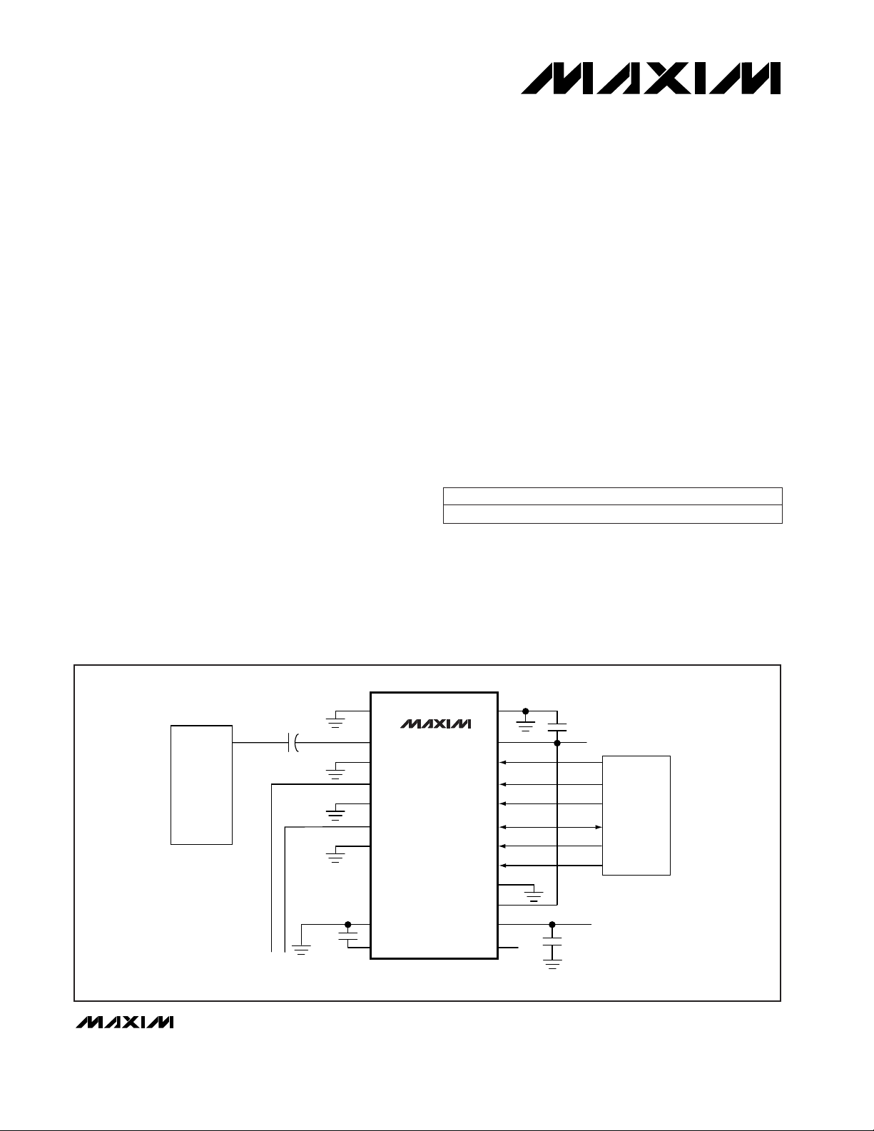
MAX1101
Single-Chip, 8-Bit CCD Digitizer
with Clamp and 6-Bit PGA
________________________________________________________________
Maxim Integrated Products
1
GND
V
DD
V
DD
0.1µF
0.1µF
0.1µF
24
22
23
21
20
19
18
17
16
15
14
13
1
2
3
4
5
6
GND
CLAMP
+5V DC (SUPPLY)
+5V DC (REFERENCE)
VIDSAMP
LOAD
DATA
SCLK
MODE
GND
REFBIAS
REF+
AIN2
REFGND
REF-
AIN1
GND
GND
GND
CCDIN
C
EXT
0.047µF
AUXILIARY
ANALOG INPUTS
CCD
ARRAY
7
11
1
2
12
MAX1101
µP/µC/
STATE LOGIC
___________________________________________________Typical Operating Circuit
19-1166; Rev 0; 12/96
PART
MAX1101CWG 0°C to +70°C
TEMP. RANGE PIN-PACKAGE
24 Wide SO
______________Ordering Information
Pin Configuration appears on last page.
For free samples & the latest literature: http://www.maxim-ic.com, or phone 1-800-998-8800
MAX1101
Single-Chip, 8-Bit CCD Digitizer
with Clamp and 6-Bit PGA
2 _______________________________________________________________________________________
ABSOLUTE MAXIMUM RATINGS
ELECTRICAL CHARACTERISTICS
(VDD= V
REFBIAS
= +4.75V to +5.25V, REFGND = 0V, REF- bypassed to REFGND with 0.1µF, C
EXT
= 47nF, TA= T
MIN
to T
MAX
,
unless otherwise noted.)
Stresses beyond those listed under “Absolute Maximum Ratings” may cause permanent damage to the device. These are stress ratings only, and functional
operation of the device at these or any other conditions beyond those indicated in the operational sections of the specifications is not implied. Exposure to
absolute maximum rating conditions for extended periods may affect device reliability.
VDDto GND............................................................-0.3V to +12V
All Pins to GND...........................................-0.3V to (V
DD
+ 0.3V)
Current into Every Pin (except V
DD
).................................±20mA
Current into V
DD
...............................................................±50mA
Continuous Power Dissipation (T
A
= +70°C)
SO (derate 11.76mW/°C above +70°C)......................941mW
Operating Temperature Range...............................0°C to +70°C
Storage Temperature Range.............................-65°C to +150°C
Lead Temperature (soldering, 10sec).............................+300°C
V
WHITE
=
(V
REF+
- V
REF-
) / G
PGA
nA1 50I
L(CCDIN)
Input Leakage (Note 2)
Ω60 150R
ON(BSS)
Black Sample Switch On-Resistance
% Gain±5PGA Gain Error
V/V0.125Gain Adjust Step Size
Steps64Gain Adjust Resolution
V/V-9.375 -9.875 -10.375Maximum PGA Gain Setting
V/V-1.9 -2 -2.1Minimum PGA Gain Setting
V
0.25
V
WHITE
Maximum Peak CCD
Differential Signal Range
1.25
LSB±0.5 ±1DNLDifferential Nonlinearity
Bits8NResolution
ns10t
AP
Aperture Delay
MHz1Input Full-Power Bandwidth
kHz1Minimum Sample Rate
MHz0.67 1.2f
s
Maximum Sample Rate
LSB±1 ±1.5INLIntegral Nonlinearity
LSB±2.5TUETotal Unadjusted Error
%µV/°C125TCVOSZero-Scale Drift
%FS/°C0.016TCFSFull-Scale Drift
UNITSMIN TYP MAXSYMBOLPARAMETER
Including black sample switch off-leakage
No-missing-codes guaranteed
G
PGA
= -10
G
PGA
= -2
VIN= 2.5Vp-p
(Note 1)
Best straight-line fit
CONDITIONS
CCD Interface Offset Voltage V
OS(CCD)VVIDEO
= V
RESET
(Figure 4) 0 4 8 LSB
Input Voltage Range V
IN
V
REF-
V
REF+
V
C
IN(ON)
Channel on 45
Input Capacitance (Note 1)
C
IN(OFF)
Channel off 10
pF
On-Resistance R
ON
120 Ω
ANALOG-TO-DIGITAL CONVERTER
ANALOG INPUT—CCD INTERFACE
ANALOG INPUT—AUXILIARY INPUTS
MAX1101
Single-Chip, 8-Bit CCD Digitizer
with Clamp and 6-Bit PGA
_______________________________________________________________________________________ 3
ELECTRICAL CHARACTERISTICS (continued)
(VDD= V
REFBIAS
= +4.75V to +5.25V, REFGND = 0V, REF- bypassed to REFGND with 0.1µF, C
EXT
= 47nF, TA= T
MIN
to T
MAX
,
unless otherwise noted.)
V1.5V
IL
Digital Input Voltage Low
V3.5V
IH
Digital Input Voltage High
mA20 40I
DD
Supply Current
dB48 60PSRRPSRR, PGA and ADC
V4.75 5 5.25V
DD
Positive Supply-Voltage Range
V0.49 0.50 0.51V
REF-
Negative Reference Voltage
V2.94 3.00 3.06V
REF+
Positive Reference Voltage
UNITSMIN TYP MAXSYMBOLPARAMETER
Internally generated, V
REFBIAS
= 5V
4.75V ≤ VDD≤ 5.25V
Internally generated, V
REFBIAS
= 5V
CONDITIONS
Digital Input Leakage Current I
IL
-10 10 µA
Digital Output Voltage High V
OH
I
SOURCE
= 4mA VDD- 0.5 V
Digital Output Voltage Low V
OL
I
SINK
= 4mA 0.5 V
Digital Output Leakage Current I
OL
Output in high-impedance mode -10 10 µA
SCLK Frequency f
SCLK
10 MHz
VIDSAMP Pulse Width t
VS
500 ns
VIDSAMP to CLAMP Separation t
VB
50 ns
LOAD Pulse Width t
LD
50 ns
VIDSAMP Fall to SCLK Rise Time t
VLS
MODE = 1 50 ns
VIDSAMP Fall to DATA t
VLD
MODE = 1 60 ns
SCLK Rise to DATA t
SD
60 ns
DATA Set-Up Time t
DSU
20 ns
DATA Hold Time t
DH
20 ns
LOAD Fall to SCLK Rise Time t
LS
MODE = 0 50 ns
SCLK Rise to LOAD Rise Time t
SL
MODE = 0 50 ns
MODE Setup Time t
MSU
Same as bus-relinquish time 50 ns
CLAMP Pulse Width t
BS
300 ns
CLAMP Fall to Video Update t
BC
(Note 1) 20 ns
Digital Quiet Time (Note 3) t
Q
± around VIDSAMP falling edge 20 ns
SCLK Pulse Width t
SPW
50 ns
Reset to CLAMP Separation t
RB
(Note 2) 50 ns
Note 1: Due to leakage in the PGA and ADC, operation at sample rates below 1ksps is not recommended, as
performance may degrade, particularly at high temperatures.
Note 2: Production test equipment settling time prohibits leakage measurements below 1nA.
Lab equipment has shown the MAX1101 switch input leakage below 1pA at T
A
= +25°C, and below 50pA at TA= +70°C.
Note 3: Not a test parameter. Recommended for optimal performance.
VIDSAMP to Reset Separation t
VR
(Note 2) 50 ns
REFERENCE VOLTAGE INPUT
POWER SUPPLIES
DIGITAL INPUTS/OUTPUTS
DIGITAL TIMING SPECIFICATIONS (t
r
r
, tf≤ 10ns, CL≤ 50pF, unless otherwise noted)
MAX1101
Single-Chip, 8-Bit CCD Digitizer
with Clamp and 6-Bit PGA
4 _______________________________________________________________________________________
______________________________________________________________Pin Description
NAME FUNCTION
1, 3, 5, 7,
10, 16, 24
GND Ground
2 CCDIN CCD Input. Connect CCD through a series 0.047µF capacitor (C
EXT
).
PIN
4 AIN1 Auxiliary Analog Input Channel 1
6 AIN2 Auxiliary Analog Input Channel 2
12 REF-
Lower Limit of Reference Span. Sets the zero-code voltage. Range is GND ≤ REF- ≤ REF+.
Nominally 0.5V.
11 REFGND Reference Ground. Ground reference for all analog signals.
8, 9, 10 I.C. Internally Connected. Do not connect to this pin.
18 SCLK Serial Clock Input
17 MODE
Control Input. Set high, DATA is an output of the ADC. Set low, DATA enables programming of the
PGA and mux.
15, 23 V
DD
Power Supply, +5V. Bypass to ground very close to the device and connect the two pins together,
close to the MAX1101.
14 REFBIAS Reference Power Supply. Connect to external +5.0V to set V
REF+
to +3.0V and V
REF-
to +0.5V.
13 REF+
Upper Limit of Reference Span. Sets the full-scale input. Voltage range is REF- ≤ REF+ ≤ VDD.
Nominally 3.0V.
19 DATA Data Input or Output, as controlled by MODE
20 LOAD Control Input. Loads serial shift-register data to PGA and multiplexer registers when MODE = 0.
21 VIDSAMP Control Input. Samples the video level and initiates the ADC conversion.
22 CLAMP Control Input. Samples black level. Can be used for correlated double sampling.
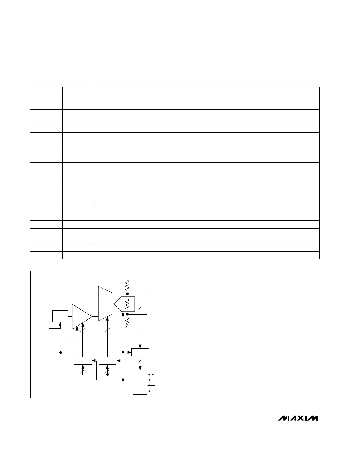
_______________Detailed Description
Overview
The MAX1101 directly processes the pixel stream from
a monochrome CCD, and removes black level, offset,
and noise errors through an internal clamp circuit,
which can be used as a correlated double sampler
(CDS). It uses a 6-bit, programmable-gain amplifier
(PGA) to adjust gain. A three-input multiplexer (mux)
selects either the PGA output or two unassigned inputs
(AIN1, AIN2). The processed analog signal is digitized
by an 8-bit, half-flash analog-to-digital converter (ADC),
and output serially through the DATA pin.
Digital data is input and output through the bidirectional
serial pin (DATA) synchronously with the external serial
clock (SCLK). When MODE = 0, the mux channels and
the PGA gain can be programmed via DATA. With MODE
= 1 (high), ADC serial data is output through this pin.
PGA
GAIN
CLAMP
CIRCUIT
MUX
ADC
REGISTER
REGISTER
6 2
6
2
1
0
2
8
8
SERIAL
PORT
DATA
SCLK
LOAD
MODE
REFBIAS
REF+
REF-
REFGND
AIN2
AIN1
CLAMP
CCDIN
VIDSAMP
REGISTER
Figure 1. MAX1101 Functional Diagram

MAX1101
Single-Chip, 8-Bit CCD Digitizer
with Clamp and 6-Bit PGA
_______________________________________________________________________________________ 5
Programmable-Gain Amplifier
The PGA amplifies the differential video signal from the
CCD (at CCDIN). Gain is settable with the 6-bit control word from -2 to -10 in 64 steps, in increments of
-0.125. The PGA also provides for periodic DC restoration of the capacitively coupled input.
As shown in Figure 2, the switched-capacitor amplifier’s
gain is set by the ratio CI/CF. The input is sampled on
the CIcapacitors, which is a set of equal capacitors.
The 6-bit gain control word determines the number
of capacitors used. Thus the PGA gain is set from
-2 to -10.
A voltage equal to V
REF-
is applied to the PGA’s noninverting input. This offsets the PGA output to be within
the range of the ADC (V
REF-
to V
REF+
).
Clamp Circuit
As shown in Figure 2, the CCD output is connected to
the MAX1101 input (CCDIN) through an external
capacitor, which removes the potentially large DC
common-mode voltages from the input signal.
Whenever CLAMP is high, the CLAMP switch is closed
and C
EXT
is charged to V
REF+
. It can be actuated
either once per pixel (sampling reset level) or less frequently (such as for restoring optical black level once
per line), as required by the application.
VIDSAMP controls the sampling of the video signal
and offset nulling of the PGA. To null out the offset,
VIDSAMP causes switches S1 and S1P to close, placing the amplifier in a unity-gain configuration, as shown
in Figure 3a. This configuration causes the amplifier’s
offset voltage to be stored on CF. In the next portion of
the cycle, when VIDSAMP returns low, the S1 switches
are opened and S2 is closed (Figure 3b). This is the
standard inverting op-amp configuration. The only difference is that capacitors are used to set the gain, and
the amplifier’s offset voltage has been stored on these
capacitors and is thus canceled. The amplifier’s output
is [C
F/CI
] x V
VIDEO
+ V
REF-
. The CDS function is shown
in Figure 4.
ADC
The ADC uses a recycling half-flash conversion technique in which a 4-bit flash ADC section achieves an
8-bit result in two steps (Figure 5). Using 15 comparators, the flash ADC compares the unknown input
voltage to the reference ladder (using REF+ and REF-)
and provides the upper four data bits.
An internal digital-to-analog converter (DAC) uses the
four most significant bits (MSBs) to generate the analog
result from the first flash conversion and a residue voltage that is the difference between the unknown voltage
Figure 2. PGA Functional Diagram
S1
S2
S1P
C
I
S2
S1CLAMP
CF
C
EXT
0.047µF
REF-
REF-
REF+ REF+
TO
ADC
FROM
CCD
VIDSAMP
S1
S2
S1P
ON
ON
ON
OFF
OFF
OFF
* INTERNALLY GENERATED SIGNALS
*
*
*
Figure 3a. PGA Connection with VIDSAMP = Low
Figure 3b. PGA Connection with VIDSAMP = High
REF+
REF-
C
F
C
I
= V
V
OUT
REF-
C
F
C
V
+
REF
- V
VIDEO
(FROM DC
RESTORE)
I
REF-
REF
- ±V
0S

MAX1101
Single-Chip, 8-Bit CCD Digitizer
with Clamp and 6-Bit PGA
6 _______________________________________________________________________________________
and the DAC output. The residue is then compared
again with the flash comparators to obtain the lower
four data bits.
Single-shot timers control the timing of the two conversion steps. Once both MSBs and LSBs have been
determined, the comparators return to input-acquisition/auto-zero mode.
REF+ and REF-
The REF+ and REF- pins set the ADC’s full-scale range.
The optimum input range is +0.5V to +3.0V. Figure 6
shows a matched resistive ladder that generates the
reference voltages. Four pins are available: REF+,
REF-, REFBIAS, and REFGND. If 5.00V is applied to
REFBIAS while REFGND is grounded, then 3.00V and
0.50V are generated at REF+ and REF-, respectively.
For increased accuracy or power-supply immunity,
REF+ can be connected to an external +3.00V reference. If this is done, the accuracy must be better than
±5%. REFBIAS should be left open in this case.
Multiplexer
The mux selects either the output of the PGA or one of
two other inputs to the ADC. The mux switching is
break-before-make to prevent transient shorts between
channels. The first two bits of the input control byte
select the mux input channel (Table 1).
Serial-Interface Logic
The serial interface inputs and outputs data in 8-bit
words. The interface is controlled by four signals:
MODE, LOAD, DATA, and SCLK.
Figure 4. Correlated Double Sampler (CDS)
CCD OUTPUT
V
VIDEO
CCD OUTPUT
LEVELS VARY
DUE TO CCD
RESET NOISE
VOLTAGE OF
RESET SECTION
IS SET TO V
REF+
BY CLAMP
CLAMP PULSE
(CLAMP)
CLAMP OUTPUT
SAMPLE-AND-HOLD PULSE
(VIDSAMP)
Figure 5. ADC Functional Diagram
OUTPUT
REGISTER
4-BIT
FLASH
ADC
4-BIT
DAC
4-BIT
FLASH
ADC
(4LSB)
VREF+
16
REF+
REF-
FROM
MUX
DATA
OUT

MAX1101
Single-Chip, 8-Bit CCD Digitizer
with Clamp and 6-Bit PGA
_______________________________________________________________________________________ 7
MODE
MODE controls the direction of data transfer. When
MODE = 0, data is being shifted into the MAX1101 at
the DATA pin either for the mux or the PGA. When
MODE = 1, the ADC output is shifted out from the
MAX1101 at the DATA pin. Data is shifted in and out of
the MAX1101 at the rising edge of SCLK.
LOAD
LOAD is normally low and used only when MODE = 0.
Once all eight bits have been clocked in, bring LOAD
high to update the MAX1101 registers.
DATA
DATA is a bidirectional I/O pin. MODE controls the
direction of data transfer. When MODE = 1, DATA is
configured as an output from the shift register. Data is
clocked out of the shift register by SCLK’s rising edge.
When MODE = 0, DATA is configured as an input to the
shift register, shifted in by the rising edge of SCLK. In
this mode, the DATA output driver is disabled, putting
DATA into a high-impedance state and allowing it to be
driven externally.
Data Output
Data is clocked in and out of the device with the rising
edge of SCLK. The first bit (the MSB, D7) immediately
follows the falling edge of VIDSAMP (Figures 7 and 8).
The first rising edge of SCLK clocks out the next bit,
D6. Data is loaded into the shift register at the falling
edge of VIDSAMP. Following the output of D0, DATA
output is unspecified for additional SCLK pulses.
Eight-bit-wide storage and output registers hold data
from the ADC and delay the data output. The timing diagram in Figure 9 shows the data latency of two
VIDSAMP cycles. New data is available after the second
falling edge of VIDSAMP.
Data Input
During data input, the first two bits (A0, A1) are the
address, selecting either the mux or PGA. The next six
bits set the input channel or PGA gain (Table 1).
CLAMP and VIDSAMP
The last two digital inputs are VIDSAMP and CLAMP.
VIDSAMP controls the overall cycle timing, with one
VIDSAMP cycle corresponding to one CCD pixel. The
input is sampled into the ADC by the falling edge of
VIDSAMP. CLAMP controls the black sample switch,
which sets a reference DC voltage level (V
REF+
) at the
capacitively coupled CCDIN input. The sample switch
is on when CLAMP is high.
Control and Interface Logic
The control and interface logic consists of a serial I/O
port, which shifts data into and out of the MAX1101, and
two registers for storing the mux channel and the PGA
gain data.
Table 1. Control-Byte Format
REFBIAS
REF+
REF-
REFGND
200Ω
1kΩ
800Ω
Figure 6. Reference Resistor String
X = Don’t Care
11111110Set PGA Gain to -9.875
01111110Set PGA Gain to -9.750
10000010Set PGA Gain to -2.125
00000010Set PGA Gain to -2
XXX00100Select AIN2
XXX01000Select AIN1
XXX00000Select CCD input
XXXXXXX1No Operation
——————10Address CCD PGA
——————00Address Analog Input Mux
D0
LSB
D1D2D3D4
D5
MSB
A1A0FUNCTION

MAX1101
Single-Chip, 8-Bit CCD Digitizer
with Clamp and 6-Bit PGA
8 _______________________________________________________________________________________
LOAD controls the loading of data into the internal storage registers during data input. Once all eight input bits
have been clocked into the shift register, a rising edge on
LOAD clocks the data into the appropriate storage register (mux or PGA), decoded from the first two input bits.
The logic is divided into four blocks: the two storage registers, the serial I/O port, and a power-on reset generator. The registers are reset by the power-on reset to
place them in a predictable state (input channel = CCD,
PGA gain = -2) on power-up. The power-on reset typically has a 2.1µs pulse width.
The serial I/O port consists of a shift register, an 8-bit
storage register, decode logic to clock input data into
the appropriate storage register, and an output driver.
The 8-bit storage register takes input data from the
ADC.
Input Buffers and Output Drivers
The DATA driver is capable of driving 50pF load capacitance while meeting the output delay specifications
given in the
Electrical Characteristics
. The gates of the Pchannel and N-channel drivers are driven separately. If
MODE is low, both drivers are off and the output is high
impedance.
The VIDSAMP, CLAMP, SCLK, and LOAD inputs are
buffered and have hysteresis to reject noise with slowslewing signal edges.
__________Applications Information
MAX1101 Timing
Figure 7 shows the timing configuration when MODE =
0 and data is loaded into the MAX1101. Figure 8 shows
timing when MODE = 1 and the CCD signal is digitized.
Figure 9 is an expansion of Figure 8, illustrating the
two-VIDSAMP-cycle data latency. Figure 10 shows the
relationship of CLAMP to VIDSAMP when MODE = 1.
MODE
SCLK
LOAD
t
MSU
t
SPW
t
SPW
t
SL
t
LD
t
LS
t
DSU
A0 A1 D5 D4 D3 D2 D1 D0
t
DH
DATA
Figure 7. MODE = 0 Timing
CCD OUT
VIDSAMP
D6 D5D7
CLAMP
SCLK
DATA
D4 D3 D2 D1 D0
RESET FEEDTHROUGH
PRECHARGE LEVEL
VIDEO LEVEL
t
CPW
t
VB
t
BS
t
VS
t
RB
t
BC
t
VB
t
VLS
t
VLD
t
SD
DATA OUTPUT AFTER D0 IS UNSPECIFIED
t
Q
t
VR
Figure 8. MODE = 1 Timing

MAX1101
Single-Chip, 8-Bit CCD Digitizer
with Clamp and 6-Bit PGA
_______________________________________________________________________________________ 9
Input/Output Transfer Function
CCD Input
Figure 11 shows the MAX1101 transfer function for
CCDIN. Coding is binary, with a -4LSB offset added to
ensure that offsets within the MAX1101, which can be
positive or negative, do not cause the ADC to be out of
range. Full-scale input range at CCDIN is:
(V
REF+
- V
REF-
) / G
PGA
where G
PGA
is the gain of the programmable gain
amplifier.
Analog Inputs (AIN_)
The transfer function for auxiliary inputs is shown in
Figure 11. Again, coding is binary and full-scale range
is V
REF-
to V
REF+
. An offset has not been added to
these channels; however, code transitions occur at the
1/2LSB point, as shown in Figure 12.
Implementing Correlated
Double Sampling (CDS) or
Black-Level Compensation
The CLAMP circuit in the MAX1101 can be used to either
accomplish CDS or to compensate for the CCD black
level. To accomplish CDS, CLAMP is activated once per
CCD (OUT)
VIDSAMP
CLAMP
DATA
SCLK
SHIFT REG
ADC REG
ADC
PGA
D6 D5 D4 D3
DATA N-3
DATA N-2
DATA N-2
DATA N-1
DATA N
DATA N+1
DATA N-1
DATA N
LSB N-1MSB N-1 LSB NMSB N LSB N+1MSB N+1 LSB N+2MSB N+2
AUTO-ZERO SAMPLE N
VIDEO N VIDEO N+1 VIDEO N+2 VIDEO N+3
SAMPLE N
SAMPLE N+1 SAMPLE N+2 SAMPLE N+3
SAMPLE N+1 SAMPLE N+2 SAMPLE N+3
AUTO-ZERO AUTO-ZERO AUTO-ZERO
D2 D1 D0D7 D6 D5 D4 D3 D2 D1 D0D7 D6 D5 D4 D3 D2 D1 D0D7 D6 D5 D4 D3 D2 D1 D0D7 D7
DATA N-3 DATA N-2 DATA N-1 DATA N
Figure 9. MODE = 1 Timing Showing Data Latency
BLACK CELL BLACK CELL
VIDEO N
CCD (OUT)
VIDSAMP
CLAMP
(ONCE PER LINE)
CLAMP
(ONCE PER CELL)
Figure 10. MODE = 1 Timing Showing Relationship of CLAMP to VIDSAMP

MAX1101
Single-Chip, 8-Bit CCD Digitizer
with Clamp and 6-Bit PGA
10 ______________________________________________________________________________________
pixel during the CCD output waveform’s reset phase. To
compensate for the CCD black level, CLAMP is activated
during the black-pixel portion of the linear array, as
shown in Figure 10. Each of these modes requires a different value of C
EXT
, as described in the following sec-
tion.
Choosing C
EXT
for CDS
In CDS applications, C
EXT
= 4nF. This value is the best
compromise to minimize errors due to the CLAMP switch
resistance/C
EXT
time constant and switch charge injection. The following equation represents the error due to
incomplete charging of C
EXT
during integration time:
ε = ∆V
RESET
x e
-t/RC
where ∆V
RESET
= the maximum change in reset level
from one pixel to the next, t = CLAMP pulse width, and
R = CLAMP switch resistance (150Ωmax). At a sample
rate of 670kHz, with t = 750nsec, a 4nF capacitor
removes at least 70% of the change in reset voltage
level. Typically, R = 60Ω, which corresponds to a 96%
cancellation of the change in reset level.
The offset due to switch charge injection is represented
by 13pC / 4nF = 3mV. Note that this error will behave
like any DC offset; that is, it will be constant from pixel
to pixel.
Choosing C
EXT
in Black-Level Compensation
In activating CLAMP once per line to compensate for the
CCD black level, the recommended value of C
EXT
is
governed by the following equations:
C
EXT
≥ 12nF
and
C
EXT
≤ N x t x 760pF/µsec
where N is the number of light-shielded cells, and t is
the width of the CLAMP pulse in µsec.
The second equation ensures that the time constant
formed by R x C
EXT
is small enough that the black level
is captured to within 0.5mV during the dark pixel
phase. For example, in an array with 27 dark pixels at a
670kHz sample rate, with t = 750nsec, the second
equation becomes C
EXT
≤ 15nF. Capacitors smaller
than 12nF can be used; however, offset increases due
to switch charge injection, as explained in the section
Choosing C
EXT
for CDS
.
11. . .111
DIGITAL
OUTPUT
11. . .110
11. . .101
100. . .000
00. . .111
00. . .110
00. . .101
00. . .100
00. . .011
00. . .010
00. . .001
00. . .000
249
256
V
FS
251
256
V
FS
124
256
V
FS
3
256
V
FS
-3
256
V
VIDEO
= VOLTAGE DIFFERENCE BETWEEN THE
VIDEO LEVEL AND THE PRE-CHARGE (RESET) LEVEL.
V
FS
-4
256
V
FS
1
256
V
FS
-1
256
V
FS
2
256
V
FS
-2
256
V
FS
250
256
V
FS
G
PGA
V
FS
=
V
REF+
- V
REF-
V
VIDEO
Figure 11. Transfer Function for CCDIN
Figure 12. Transfer Function for AIN
111. . . . 111
DIGITAL
OUTPUT
111. . . . 110
111. . . . 101
100. . . 000
000. . . 011
000. . . 010
000. . . 001
000. . . 000
V
REF-
253
256
V
FS
255
256
V
FS
3
256
V
FS
1
256
V
FS
2
256
V
FS
4
256
V
FS
254
256
V
FS
V
FS
= V
REF+
- V
REF-
V
AIN_

MAX1101
Single-Chip, 8-Bit CCD Digitizer
with Clamp and 6-Bit PGA
______________________________________________________________________________________ 11
__________________Pin Configuration
___________________Chip Information
Bypassing and Layout Considerations
Solder the MAX1101 to a multilayer board (two or more
layers) where the layer immediately beneath the device
is a ground plane.
Connect the VDDpins together at the MAX1101. Connect
all ground pins together at the device.
Bypass VDDto ground with at least a 0.1µF ceramic
capacitor. If larger capacitors are used, tantalum is
satisfactory.
0.01
3 10
100.00
MAX1101-FIG13
NUMBER OF TIME CONSTANTS
ERROR (BITS)
9
1.00
0.10
5 7
10.00
4 6 8
Figure 13. Black Level Error vs. C
EXT
Time Constant at
Maximum PGA Gain (1mV/bit)
TRANSISTOR COUNT: 3430
24
23
22
21
20
19
18
17
1
2
3
4
5
6
7
8
GND
V
DD
BLKSAMP
VIDSAMPAIN1
GND
CCDIN
GND
TOP VIEW
LOAD
DATA
SCLK
MODEI.C.
GND
AIN2
GND
16
15
14
13
9
10
11
12
GND
V
DD
REFBIAS
REF+REF-
REFGND
I.C.
I.C.
SO
MAX1101

Maxim cannot assume responsibility for use of any circuitry other than circuitry entirely embodied in a Maxim product. No circuit patent licenses are
implied. Maxim reserves the right to change the circuitry and specifications without notice at any time.
12
__________________Maxim Integrated Products, 120 San Gabriel Drive, Sunnyvale, CA 94086 (408) 737-7600
© 1996 Maxim Integrated Products Printed USA is a registered trademark of Maxim Integrated Products.
MAX1101
Single-Chip, 8-Bit CCD Digitizer
with Clamp and 6-Bit PGA
Maxim cannot assume responsibility for use of any circuitry other than circuitry entirely embodied in a Maxim product. No circuit patent licenses are
implied. Maxim reserves the right to change the circuitry and specifications without notice at any time.
12
__________________Maxim Integrated Products, 120 San Gabriel Drive, Sunnyvale, CA 94086 (408) 737-7600
© 1996 Maxim Integrated Products Printed USA is a registered trademark of Maxim Integrated Products.
________________________________________________________Package Information
SOICW.EPS
 Loading...