

Page 1
General Description
The MAX105 evaluation kit (EV kit) is a fully assembled
and tested circuit board that contains all the components necessary to evaluate the performance of the
MAX105, dual channel, 6-bit (800Msps), or the
MAX107, dual channel, 6-bit (400Msps) high-speed
analog-to-digital converter (ADC). The MAX105 ADC is
able to process differential or single-ended analog
inputs. The EV kit allows the user to evaluate the ADC
with either type of signals. The digital output produced
by the ADC can be easily sampled with a user-provided high-speed logic analyzer or data-acquisition system. The EV kit comes with the MAX105 installed. To
evaluate the MAX107, replace the MAX105 with the
MAX107.
Features
♦ Two Matched 6-Bit, 800 Msps ADCs
♦ 0.8V
p-p
Input Signal Range
♦ Demultiplexed Differential LVDS Outputs
♦ Square-Pin Headers for Easy Connection of Logic
Analyzer to Digital Outputs
♦ Four-layer PC Board with Separate Analog and
Digital Power and Ground Connections
♦ Fully Assembled and Tested with MAX105
Installed
Evaluates: MAX105/MAX107
MAX105 Evaluation Kit
________________________________________________________________ Maxim Integrated Products 1
19-2055; Rev 0; 5/01
ADC Selection Table
Ordering Information
Component List
Component Suppliers
*Exposed pad
Note: Please indicate that you are using the MAX105 when contacting these component suppliers.
For pricing, delivery, and ordering information, please contact Maxim/Dallas Direct! at
1-888-629-4642, or visit Maxim’s website at www.maxim-ic.com.
查询MAX105EVKIT供应商
DESIGNATION QTY DESCRIPTION
C1, C5, C9,
C13, C16,
C18, C20, C22
C2, C6, C10,
C14, C15,
C17, C19,
C21,
C24–C28, C30
C3, C4, C7,
C8, C11, C12
C23, C29 2
L1–L4 4
R1–R6 6 51.1Ω ±1% resistors (0402)
R7–R32 26 100Ω ±1% resistors (0402)
J1–J6 6 SMA connectors (edge-mounted)
JU1, JU2 0 Not installed 2-pin headers
JU4–JU55 52 2-pin headers
JU3 0 Not installed 3-pin header
AVCC, AGND,
OVCC, OGND
U1 1 MAX105ECS (80-pin TQFP-EP)
None 1 MAX105 PC board
None 1 MAX105 data sheet
None 1 MAX105 EV kit data sheet
47pF ±10%, +50V COG ceramic
8
capacitors (0402)
Murata GRM36COG470K050AD
0.01µF ±10%, +16V X7R ceramic
capacitors (0402)
14
Murata GRM36X7R103K016AD
100pF ±5%, +50V COG ceramic
6
capacitors (0402)
Murata GRM36COG101J050AD
10µF ±10%, +25V tantalum
capacitors (CASE D)
AVX TAJD106K025R
Ferrite beads 600Ω at 100MHz,
500mA , 0.3Ω DCR
Murata BLM21A601R
4 Test point hooks
MAX105EVKIT 0°C to 70°C 80 TQFP-EP*
MAX105ECS 800
MAX107ECS 400
AVX 803-946-0690 803-626-3123
Murata 814-237-1431 814-238-0490
PART TEMP. RANGE IC PACKAGE
PART SPEED (Msps)
SUPPLIER PHONE FAX
Page 2

Evaluates: MAX105/MAX107
MAX105 Evaluation Kit
2 _______________________________________________________________________________________
Quick Start
Test Equipment Required
• DC power supplies:
Digital +3.3V, 510mA
Analog +5.0V, 350mA
• Generator with low phase-noise for clock input
(e.g., HP8662A, HP8663A, or equivalent)
• Two signal generators for analog signal inputs (e.g.,
HP8662A, HP8663A, or equivalent)
• Logic analyzer or data-acquisition system (e.g.,
HP16500C series, HP16517A 1.25Gbps state
module for single-ended evaluation.
• User-selected analog bandpass filters (e.g., TTE
Elliptical Bandpass Filter, or equivalent)
• Digital Voltmeter
• Baluns (e.g., MA/COM H-9-SMA)
•50Ω terminators with SMA connectors
The MAX105 EV kit is a fully assembled and tested surface-mount board. Follow the steps below for board
operation. Do not turn on power supplies or enable
function generators until all connections are
completed.
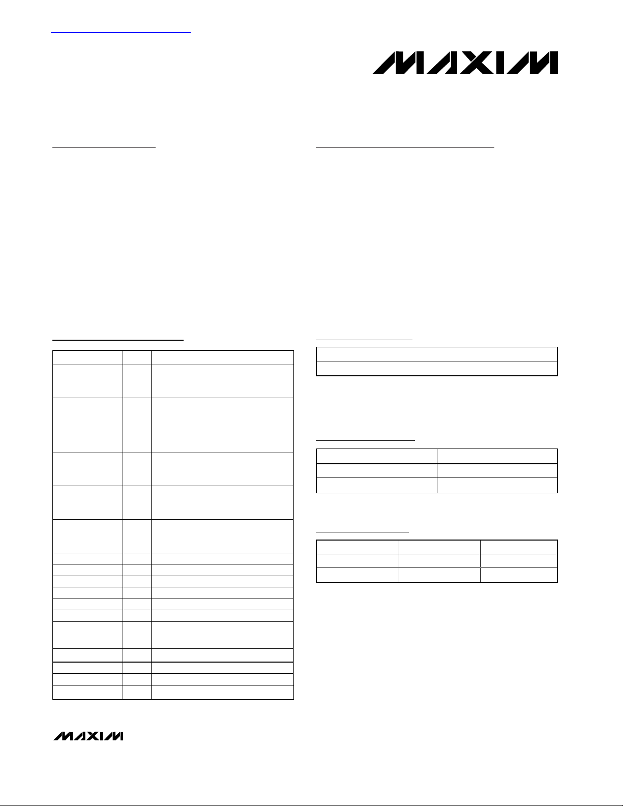
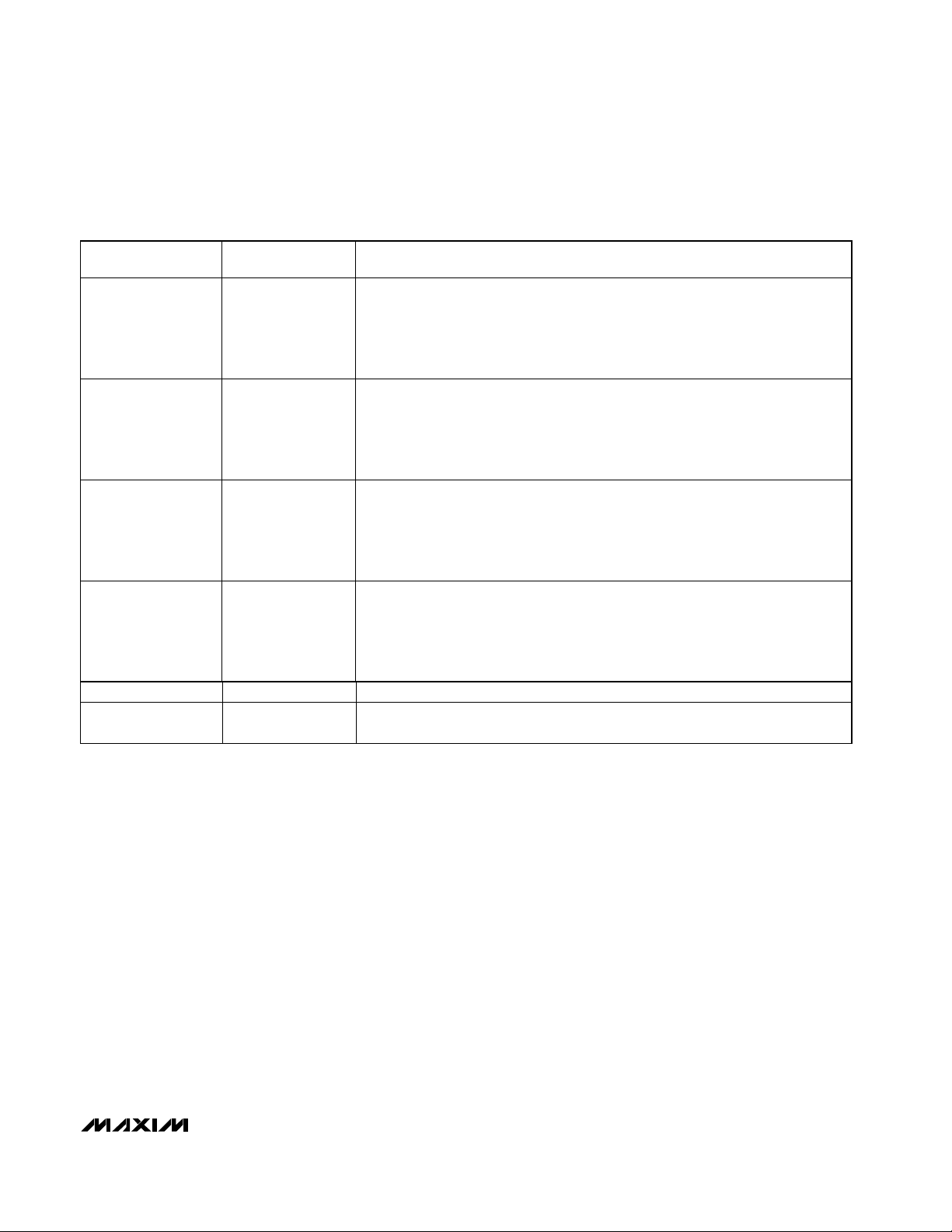
1) Connect a signal generator with low phase-jitter to
the clock inputs CLK- and CLK+ through a balun
(Figure 1). For a single-ended clock input (Figure
2), connect a 500mV (354mV
RMS
, +4dBm) amplitude from the signal generator to the CLK+ input
and terminate the unused CLK- input with a 50Ω
termination resistor to AGND.
2) For differential operation, connect a ±380mV
270mV
RMS
(approximately -0.5dB FS) sine-wave
test signal to connector A of the balun. Terminate
connector B of the balun with a 50Ω terminator.
Attach connector C of the balun to the analog input
VINI+ (VINQ+). Attach connector D of the balun to
the analog input VINI- (Figure 1). For single-ended
operation, apply the test signal to either VINI+
(VINQ+) or VINI- (VINQ-) and terminate the unused
input with a 50Ω resistor to AGND (Figure 2). For
best results, use a narrow bandpass filter designed
for the frequency of interest to reduce the harmonic
distortion of the signal generator.
3) Phase-lock both the VINI and/or VINQ signal generators with the clock generator.
4) Connect a logic analyzer, such as the HP16500 with
the HP16517 plug-in module to monitor the I or Q
channel of the MAX105. Note that the podlets are
single-ended to ground and you may need to
remove the 100Ω termination resistors R7–R32 to
increase the logic signal swing. Reflections are
absorbed by the back-terminated LVDS drivers.
Note: Two state modules are required to monitor
both I and Q channel simultaneously.
5) Connect the logic analyzer clock to the DREADY+
output on the EV kit and set the logic analyzer to
trigger on the falling edge of the DREADY+ signal.
6) Connect a +5V power supply to the pad marked
AV
CC
. Connect the supply’s ground to the pad
marked AGND.
Note: MAX105 has separate AV
CC
I and AVCCQ
supply pins.
7) Connect a +3.3V power supply to the pad marked
OV
CC
. Connect the supply’s ground to the pad
marked OGND. Tie AGND and OGND together at
the power supplies.
Note: MAX105 has separate OV
CC
I and OVCCQ
supply pins.
8) Turn on both power supplies, then the signal
sources. Capture the digitized outputs from the
MAX105 with the logic analyzer and transfer the
digital record to a PC for data analysis.
Detailed Description
The MAX105 EV kit evaluates the performance of the
MAX105 dual channel, 6-bit ADC at a maximum clock
frequency of 800MHz (400MHz for MAX107). The
MAX105 ADC can process differential or single-ended
analog and clock inputs. The user may apply baluns to
generate differential signals from a single-ended analog signal to the EV kit.
The EV kit’s PC board incorporates a four-layer board
design to optimize the performance of the MAX105 in a
50Ω environment. Separate analog and digital ground
planes minimize noise coupling between analog and
digital signals. The EV kit requires a +5.0V power supply applied to the analog power plane, and a +3.3V
power supply applied to the digital power plane.
Access to the outputs is provided through the two-pin
headers (Table 1) all around the edge of the board. A
silkscreen on the PC board’s top layer indicates reference designations.
Page 3
Power Supplies
The MAX105 EV kit requires separate analog and digital power supplies for best performance. A +3.3V ±10%
power supply is used to power the digital portion
(OVCC) of the ADC. A separate +5.0V ±5% power supply is used to power the analog portion (AVCC) of the
ADC. Ferrite beads are used to filter out high-frequency
noise at the analog power supply. At 100MHz, the ferrite beads have an impedance of 600Ω.
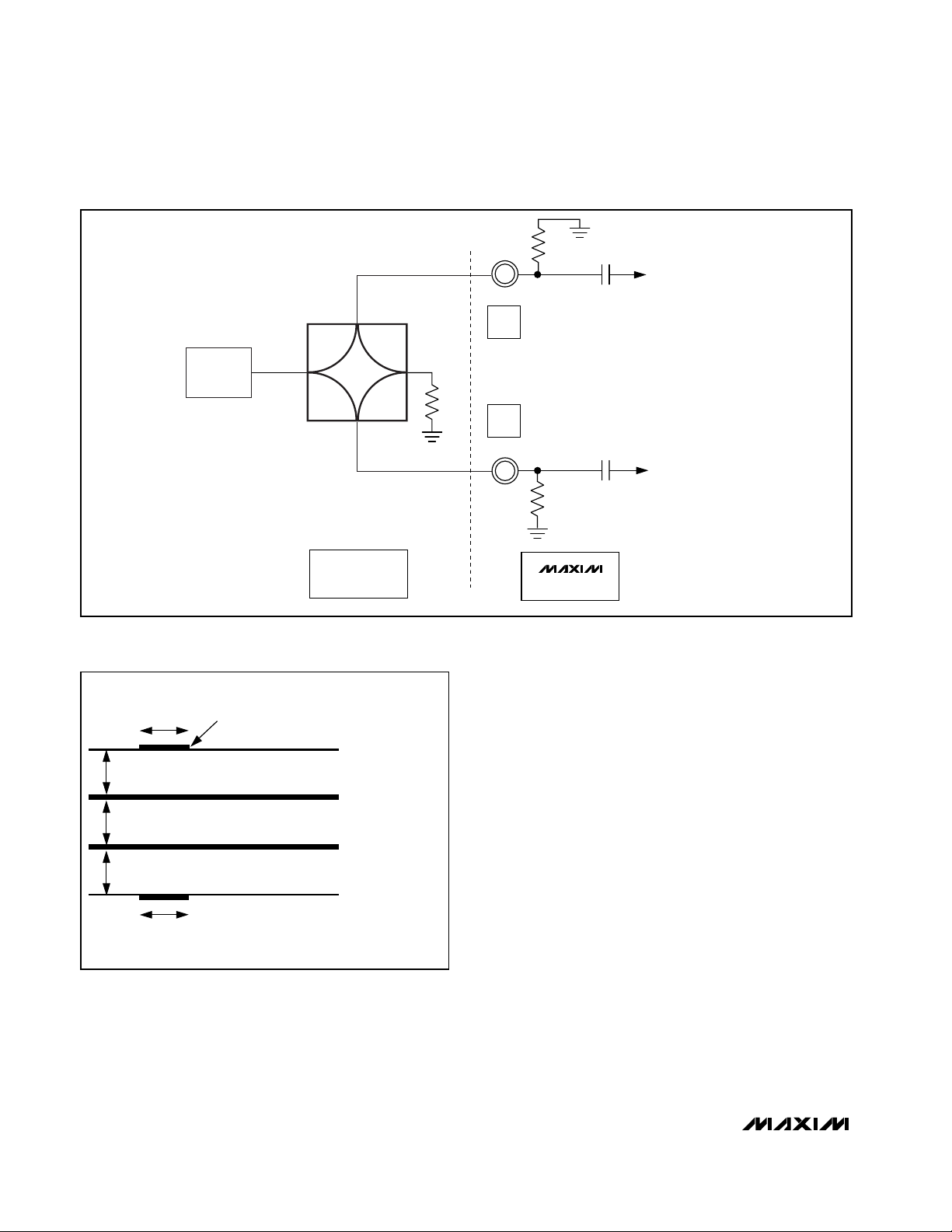
Clock
The clock signals CLK± are AC-coupled from the SMA
connectors J3 and J4. The DC-biasing level is internally
set to the reference voltage. The MAX105’s clock input
resistance is 5kΩ. However, the EV kit’s clock input
resistance is set by an external resistor to 50Ω. An ACcoupled, differential sine-wave signal may be applied
to the CLK± SMA connectors (Figure 3). The signal
must not exceed a magnitude of 1.4V
RMS
. The typical
clock frequency should be 800MHz for MAX105
(400MHz for MAX107).
I/Q Input Signals
The input signals are AC-coupled. The DC biasing level
is internally set to the reference voltage V
REF
. The
MAX105’s analog input resistance is 2kΩ per input.
However, the EV kit’s I/Q input resistance is set to 50Ω
by an external resistor. For single-ended operation,
apply a signal to one of the analog inputs and terminate
the opposite complimentary input with a 50Ω resistor to
ground.
Note: When a differential signal is applied to the ADC,
the positive and negative input pins of the ADC each
receive half of the input signal supplied to the balun. A
common mode voltage of +2.5V is established within
the part and blocked by the AC-coupling capacitors.
Evaluates: MAX105/MAX107
MAX105 Evaluation Kit
_______________________________________________________________________________________ 3
Table 1. LVDS Outputs and Functional Description
LVDS OUTPUT
SIGNALS
P5I+, P5I- (MSB)
P4I+, P4IP3I+, P3IP2I+, P2IP1I+, P1IP0I+, P0I- (LSB)
A5I+, A5I- (MSB)
A4I+, A4IA3I+, A3IA2I+, A2IA1I+, A1IA0I+, A0I- (LSB)
P5Q+, P5Q- (MSB)
P4Q+, P4QP3Q+, P3QP2Q+, P2QP1Q+, P1QP0Q+, P0Q- (LSB)
A5Q+, A5Q- (MSB)
A4Q+, A4QA3Q+, A3QA2Q+, A2QA1Q+, A1QA0Q+, A0Q- (LSB)
DOR+, DOR- JU33, JU32 Out-of-range signal’s true and complementary outputs
DREADY+,
DREADY-
EV KIT HEADER
LOCATION
JU52, JU53
JU48, JU49
JU44, JU45
JU12, JU13
JU40, JU41
JU36, JU37
JU54, JU55
JU50, JU51
JU46, JU47
JU18, JU19
JU42, JU43
JU38, JU39
JU6, JU7
JU10, JU11
JU16, JU17
JU22, JU23
JU27, JU26
JU31, JU30
JU4, JU5
JU8, JU9
JU14, JU15
JU20, JU21
JU25, JU24
JU29, JU28
JU34, JU35
FUNCTIONAL DESCRIPTION
Primary in-phase differential outputs from MSB to LSB. “+” indicates the true value,
“-” denotes the complementary outputs
Auxiliary in-phase differential outputs from MSB to LSB. “+” indicates the true
value, “-” denotes the complementary outputs
Primary quadrature differential outputs from MSB to LSB. “+” indicates the true
value, “-” denotes the complementary outputs
Auxiliary quadrature differential outputs from MSB to LSB. “+” indicates the true
value, “-” denotes the complementary outputs
Data Ready LVDS output latch clock. Output data changes on the rising edge of
DREADY+
Page 4
Evaluates: MAX105/MAX107
Reference
An on-chip reference is provided with a nominal +2.5V
output. This voltage is then processed to drive the
resistor ladder in the ADC core. A buffered reference
voltage is also used as the DC-bias voltage for the analog input.
Demultiplexing and LVDS Outputs
Each ADC provides six differential outputs (two’s complement code) at 800MHz, which fan out to 12 differential outputs at 400MHz after the on-chip demultiplexer.
To interface with lower supply CMOS DSP chips, all
outputs provide LVDS-compatible voltage levels. The
LVDS outputs will have approximately ±270mV swing
differential with a common mode around 1.25V. The differential output impedance is roughly 100Ω. For details,
refer to IEEE standard 1596.3.
*Note: To boost the output signal swing for singleended data capture with the HP16500C and HP16517A
high-speed state module, all 100Ω termination resistors (R7–R32) should be removed.
Out-of-Range (DOR) Signal
The out-of-range signal (DOR+, DOR-) flags high when
either the I or Q input is below -FS or above +FS. The
out-of-range signal has the same latency as the ADC
output data or is demultiplexed the same way. For an
800MHz system DOR+ and DOR- are clocked at
400MHz.
Data Ready (DREADY) Output
In single-ended data capture mode the clock interface
of the logic analyzer should be connected to the
DREADY output at headers JU34 or JU35 on the EV kit.
Since both the primary and auxiliary outputs change on
the rising edge of DREADY, set the logic analyzer to
trigger on the falling edge. DREADY and the data outputs are internally time aligned, which places the falling
edge of DREADY in the approximate center of the valid
data window, resulting in the maximum setup and hold
time for the logic analyzer.
Board Layout
The MAX105 EV kit is a four-layer PC board design
(Figure 4), optimized for high-speed signals. The board
is constructed from low-loss GETek core material which
has a relative dielectric constant of 3.9 (
ε
R
= 3.9). The
GETek material used in the MAX105 EV kit board offers
improved high frequency and thermal properties over
standard FR4 board material. All high-speed signals
are routed with differential microstrip transmission lines.
Special Layout Considerations
Special effort was made in the board layout to separate
the analog and digital portions of the circuit. 50Ω
microstrip transmission lines are used for analog and
clock inputs, as well as for all digital LVDS outputs. The
power plane is separated into strips to provide isolation
between different sections of the circuit (e.g., AV
CC
I and
AVCCQ or OVCCI and OVCCQ). All differential outputs are
properly terminated with 100Ω termination resistors
between true and complementary digital outputs.
The PC board comes in a circular shape to ensure the
best possible trace length matching for the 50Ω
microstrip lines. The electrical lengths of the 50Ω
microstrip lines are matched to within a few picoseconds to minimize layout-dependent delays. The propagation delay on the MAX105 EV kit board is about
130ps/inch.
The line width for a differential microstrip is 2.5mils with
a ground plane height of 14mils which is a standard
GETek core thickness. Table 2 shows PC board layers
of the EV kit.
MAX105 Evaluation Kit
4 _______________________________________________________________________________________
Table 2. MAX105 EV kit Layers
Layer I, Top Layer
Layer II, Ground
Plane
Layer III, Power
Plane
Layer IV, Bottom
Layer
LAYER DESCRIPTION
Components, Headers, Connectors,
Test Pads, AV
OGND, Analog 50Ω microstrip lines.
100Ω Termination Resistors
AGND, AGNDI, AGNDQ, AGNDR,
OGND, OGNDI, OGNDQ
AVCC, AVCCI, AVCCQ, AVCCR, OVCC,
OV
I, OVCCQ
CC
AGND, Components
, OVCC, AGND,
CC
Page 5
Evaluates: MAX105/MAX107
MAX105 Evaluation Kit
_______________________________________________________________________________________ 5
Figure 1. Typical Evaluation Setup with Differential Analog Inputs, Differential Clock Drive, and Single-Ended Data Capture
HP8662A/3A
SINE-WAVE
SOURCE
EXTERNAL 50Ω
TERMINATION TO AGND
BPF
HP8662A/3A
SINE-WAVE
SOURCE
BPF
VINI-
CLK+
CLK-
AV
CC
+5V ANALOG
AGND
+3.3V DIGITAL
DGND
AGND
OV
CC
DGND
V
IN
I+
OUTPUTS DREADY
VINQ- VINQ+
HP8662A/3A
SINE-WAVE
SOURCE
EXTERNAL 50Ω
TERMINATION TO
AGND
EXTERNAL 50Ω
TERMINATION TO
AGND
HP16500C
LOGIC ANALYZER
WITH HP16517A
1.25Gbps STATE MODULE
POWER
SUPPLIES
800MHz
+4dBm
GBIP
24 DATA
DREADY+
OR DREADY-
PHASELOCKED
PC
MAX105EVKIT
Figure 2. Typical Evaluation Setup with Single-Ended Analog Inputs, Single-Ended Clock Drive, and Single-Ended Data Capture
PHASELOCKED
HP8662A/3A
SINE-WAVE
SOURCE
HP8662A/3A
SINE-WAVE
SOURCE
HP8662A/3A
SINE-WAVE
SOURCE
PC
800MHz
+4dBm
GBIP
BPF
BPF
BPF
EXTERNAL 50Ω
TERMINATION TO AGND
EXTERNAL 50Ω
TERMINATION TO AGND
LOGIC ANALYZER
WITH HP16517A
1.25Gbps STATE MODULE
BALUN
A
BALUN
A
BALUN
A
HP16500C
C
BD
C
BD
C
BD
EXTERNAL 50Ω
TERMINATION TO
AGND
V
I-
IN
MAX105EVKIT
CLK+
CLK-
OUTPUTS DREADY
24 DATA
DREADY+
OR DREADY-
V
IN
I+
VINQ- VINQ+
AV
AGND
OV
DGND
CC
CC
+5V ANALOG
AGND
+3.3V DIGITAL
DGND
POWER
SUPPLIES
Page 6
Evaluates: MAX105/MAX107
MAX105 Evaluation Kit
6 _______________________________________________________________________________________
Figure 3. AC-Coupled, Differential Clock Drive
25mils
50Ω
50Ω
25mils
LAYER NO. 1 (TOP)
LAYER NO. 2
LAYER NO. 3
LAYER NO. 4 (BOTTOM)
1oz. Cu
14mils GETek CORE
14mils GETek CORE
GETek PREPREG AS NEEDED
Figure 4. PC Board Stacking
D
SIGNAL
SOURCE
50Ω
180°
A
0°
CONNECTION
0°
B
0°
C
AGND
EXTERNAL
50Ω
SMA
SMA
50Ω
50Ω
AGND
MAX105EVkit
AGND
TO ADC
CLK-
100pF
TO ADC
CLK+
100pF
Page 7
Evaluates: MAX105/MAX107
MAX105 Evaluation Kit
_______________________________________________________________________________________ 7
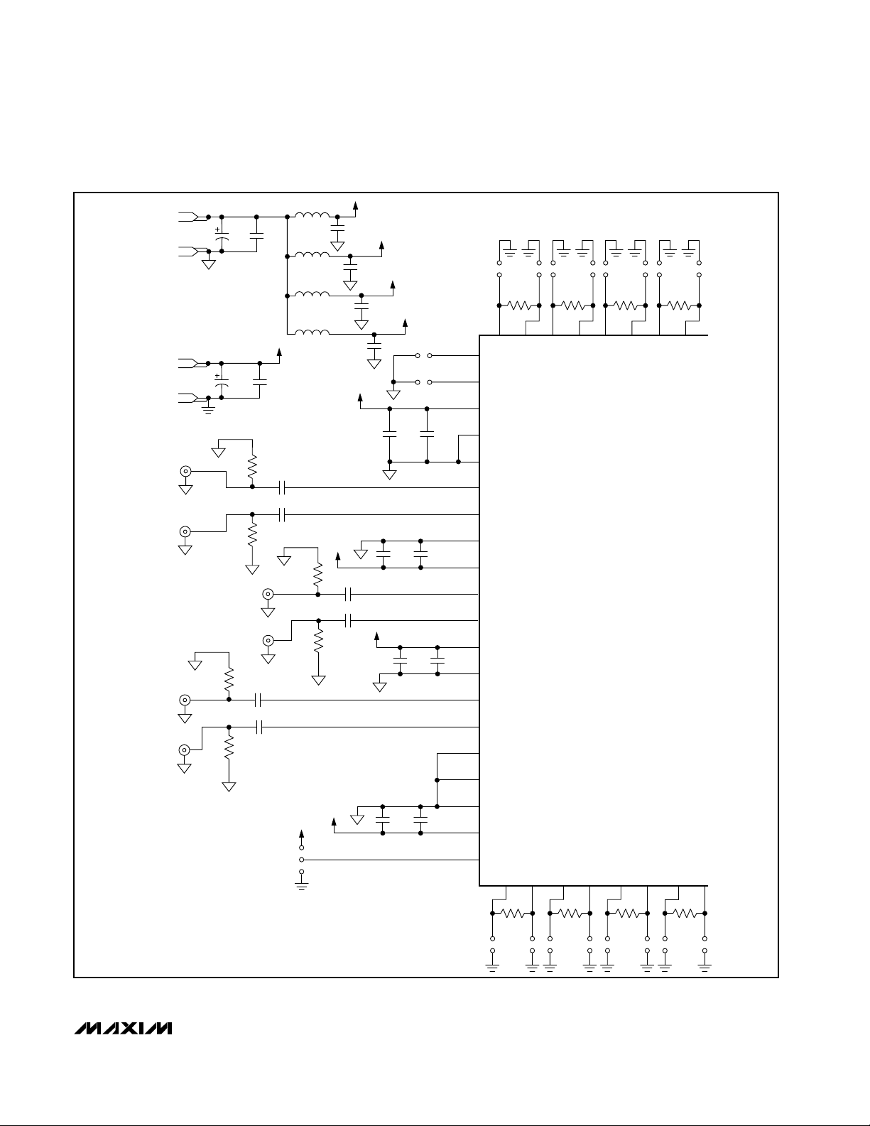
J7
Figure 5a. MAX105 EV Kit Schematic
J8
J9
J10
J1
AGND
AGND
J5
AGND
J6
AGND
J2
AGND
AGND
AGND
AGND
C23
10µF
C29
10µF
R5
51.1Ω
R6
51.1Ω
AGND
J3
J4
C24
0.01µF
R1
51.1Ω
R2
51.1Ω
AGND
AGND
C12
100pF
C11
100pF
OVCC
C30
0.01µF
AGND
JU3
C4
100pF
C3
100pF
OVCC
IND1
IND1
IND1
IND1
L1
L2
L3
L4
AGND
AVCCI
R3
51.1Ω
R4
51.1Ω
AVCC
AVCCR
C25
0.01µF
AVCCR
AGND
C8
100pF
C7
100pF
AGND
C26
0.01µF
AVCCI
C27
0.01µF
AVCCQ
AGND
AVCCQ
C28
0.01µF
AGND
AVCC
C2
0.01µF
C6
0.01µF
C14
0.01µF
C10
0.01µF
JU54 JU55
R32
100Ω
80 73747576777879
10
11
12
13
14
15
16
17
18
19
20
1
2
3
4
5
6
7
8
9
A5I+ P4I-P4I+A4I-A4I+P5I-P5I+A5I-
TEMPS
REF
R
AV
CC
AGNDR
AGNDI
V
-
INI
+
V
INI
AGNDI
I
AV
CC
CLK+
CLK-
Q
AV
CC
AGNDQ
V
Q+
IN
Q-
V
IN
AGNDQ
SUB
AGND
AV
CC
TESTB
A5Q+ P4Q-P4Q+A4Q-A4Q+P5Q-P5Q+A5Q-
21 28272625242322
JU1
JU2
C1
47pF
C5
47pF
C9
47pF
C13
47pF
JU52 JU53
R31
100Ω
JU50 JU51
R30
100Ω
JU48 JU49
R29
100Ω
R7
100Ω
JU4 JU5
R8
100Ω
JU6 JU7
R9
100Ω
JU8 JU9
R10
100Ω
JU10 JU11
Page 8

Evaluates: MAX105/MAX107
MAX105 Evaluation Kit
8 _______________________________________________________________________________________
Figure 5b. MAX105 EV Kit Schematic (continued)
OVCC
C22
47pF
C21
0.01µF
U1
JU46 JU47
R28
100Ω
JU44 JU45
R27
100Ω
C20
OVCC
47pF
JU18 JU19
C19
0.01µF
IOGNDIP3I-P3I+A3I-A3I+OGNDIOVCCI P2I-
CC
MAX105
QP3Q-P3Q+A3Q-A3Q+OGNDQOVCCQ P2Q-
CC
R14
100Ω
JU12 JU13
100Ω
6263646566676869707172 61
P2I+A2I-A2I+OV
P2Q+A2Q-A2Q+OGNDQOV
3938373635343332313029 40
R11
A1I+
A1I-
P1I+
P1I-
A0I+
A0I-
P0I+
P0I-
DREADY+
DREADY-
D0R-
D0R+
P0Q-
P0Q+
A0Q-
A0Q+
P1Q-
P1Q+
A1Q-
A1Q+
60
59
58
57
56
55
54
53
52
51
50
49
48
47
46
45
44
43
42
41
R26
100Ω
R25
100Ω
R24
100Ω
R23
100Ω
R22
100Ω
R21
100Ω
R20
100Ω
R19
100Ω
R18
100Ω
R17
100Ω
JU42
JU43
JU40
JU41
JU38
JU39
JU36
JU37
JU34
JU35
JU32
JU33
JU30
JU31
JU28
JU29
JU26
JU27
JU24
JU25
X1
MTHOLE
X2
MTHOLE
X3
MTHOLE
X4
MTHOLE
X5
LOGO
1
1
1
1
1
C16
OVCC OVCC
47pF
C15
0.01µF
R12
100Ω
JU14 JU15
R13
100Ω
JU16 JU17
C18
47pF
C17
0.01µF
R15
100Ω
JU20 JU21
R16
100Ω
JU22 JU23
Page 9
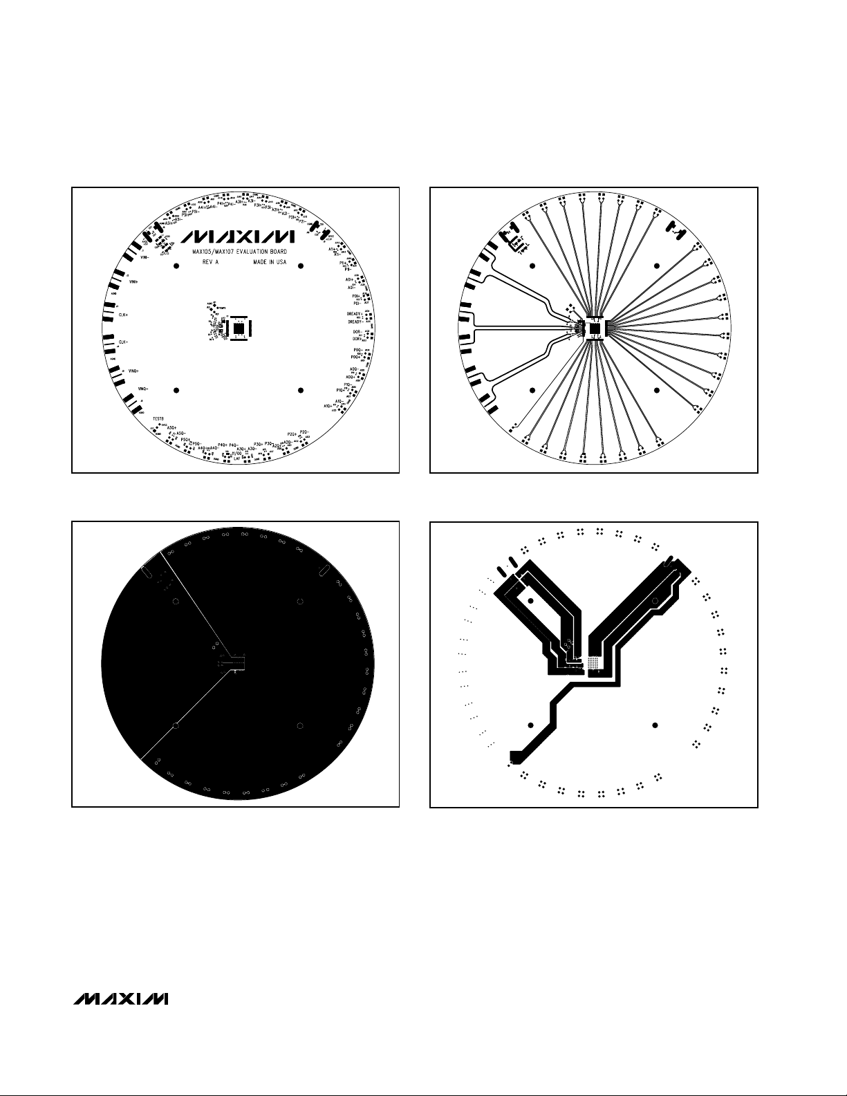
________________________________________________________________________________________________ 9
Figure 6. MAX105 EV Kit Component Placement Guide—
Component Side
Figure 7. MAX105 EV Kit PC Board Layout—Component Side
Figure 8. MAX105 EV Kit PC Board Layout—Inner Layer,
Ground Plane
MAX105 Evaluation Kit
Evaluates: MAX105/MAX107
Figure 9. MAX105 EV Kit PC Board Layout—Inner Layer,
Power Plane
Page 10

Maxim cannot assume responsibility for use of any circuitry other than circuitry entirely embodied in a Maxim product. No circuit patent licenses are
implied. Maxim reserves the right to change the circuitry and specifications without notice at any time.
10 ____________________Maxim Integrated Products, 120 San Gabriel Drive, Sunnyvale, CA 94086 408-737-7600
© 2001 Maxim Integrated Products Printed USA is a registered trademark of Maxim Integrated Products.
Evaluates: MAX105/MAX107
MAX105 Evaluation Kit
Figure 10. MAX105 EV Kit PC Board Layout—Solder Side
Figure 11. MAX105 EV Kit Component Placement Guide—
Solder Side
 Loading...