

K
g
查询DS21354DK供应商
DS21354D
T1 Single-Chip Transceiver
www.maxim-ic.com
GENERAL DESCRIPTION
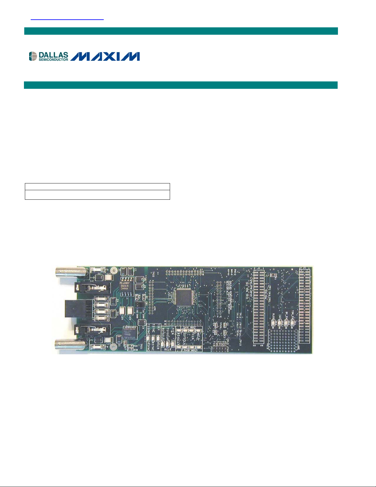
The DS21354 design kit is an evaluation board for
the DS21354. The DS21354DK is intended to be
used as a daughter card with either the DK2000 or
the DK101 motherboards. The board is complete with
a single-chip transceiver (SCT), transformers,
termination resistors, configuration switches, line
protection circuitry, network connectors, and an
interface to the motherboard.
ORDERING INFORMATION
PART DESCRIPTION
DS21354DK DS21354 Design Kit Daughter Card
Desi
n Kit Daughter Card
FEATURES
§ Expedites New Designs by Eliminating First-Pass
Prototyping
§ Interfaces Directly to the DK101 or DK2000
Motherboards
§ Demonstrates Key Functions of the DS21354
§ High-Level Software Provides Visual Access to
Registers
§ Software Controlled (Register Mapped)
Configuration Switches to Facilitate Clock and
Signal Routing
§ BNC Connections for 75W E1
§ Bantam and RJ48 Connectors for 120W T1
§ Multitap Transformer to Facilitate True
Impedance Matching for 75W and 100W/120W
Paths
§ Network Interface Protection for Overvoltage and
Overcurrent Events
§ Testpoints and Prototype Area Available for
Further Customization
1 of 20
REV: 060303

DS21354DK T1 Single-Chip Transceiver Design Kit Daughter Card
TABLE OF CONTENTS
COMPONENT LIST.....................................................................................................................3
BASIC OPERATION....................................................................................................................4
HARDWARE CONFIGURATION .................................................................................................................. 4
QUICK SETUP (DEMO MODE).................................................................................................................. 4
QUICK SETUP (REGISTER VIEW) ............................................................................................................. 4
REGISTER MAP..........................................................................................................................5
CPLD REGISTER MAP ........................................................................................................................... 5
DS21354 INFORMATION............................................................................................................7
DS21354DK INFORMATION.......................................................................................................7
TECHNICAL SUPPORT..............................................................................................................7
SCHEMATICS .............................................................................................................................7
LIST OF TABLES
Table 1. Daughter Card Address Map .........................................................................................5
Table 2. CPLD Register Map .......................................................................................................5
2 of 20

DS21354DK T1 Single-Chip Transceiver Design Kit Daughter Card
COMPONENT LIST
DESIGNATION QTY DESCRIPTION SUPPLIER PART
C1–C5, C8–C12,
C15–C19, C21,
C22, C29–C34
C7, C36 2
C13, C14 2
C23 1
C24–C27 4
C35 1
DS1, DS4–DS18 16 LED, green, SMD Digi-Key P501CT-ND
DS2, DS3 2 LED, red, SMD Digi-Key P500CT-ND
F1–F6 6 250V, 1.25A fuse, SMT Teccor Electronics F1250T
J1, J2 2 Male 0.1, SMD, 50-pin, dual-row vertical Samtec TSM-125-01-T-DV
J3, J4 2 Bantam connectors SWK RTT34B02
J5, J6 2 Connector BNC RA 5-pin Kruvand UCBJR220
J7–J9 3 Socket, SMD, 50-pin, dual-row vertical Samtec
JT10 1 Connector, 10-pin, dual-row vertical Digi-Key S2012-05-ND
L1 1
R1, R14, R21 3
R2, R3, R58, R59 4
R4, R5, R60 3
R6, R9, R10, R13,
R15–R19, R22,
R23, R25–R29,
R32, R37, R38,
R44, R47–R49, R61
R7, R8, R11, R12,
R30, R31, R35,
R36, R39–R43,
R45, R50–R53
R24 1
R33, R34 2 NOPOP — NOPOP
R46 1
R54, R55 2
R56, R57 2
RJ1 1 RJ48 connector Molex 43223
SW1 1 Switch DPDT slide 6-pin TH Avnet SSA22
T1 1 XFMR 16-pin SMT Pulse Engineering TX1099
U1–U4, U6 5 BBUS switch 10-bit CMOS, 150-mil, 24-pin SO IDT IDTQS3R861Q
U5 1 144-pin macrocell CPLD Avnet
U7–U10 4 Quad bus switch, 150-mil, 16-pin SO IDT IDTQS3125Q
U11 1 T1/E1/J1 XCVR 100-pin QFP, 0°C to +70°C Dallas Semiconductor DS2156L
Z1, Z6–Z8 4 160V, 500A Sidactor Teccor Electronics P1800SCMC
Z2, Z3 2 58V, 500A Sidactor
Z4, Z5 2 6V, 50A Sidactor
Z9, Z10 2 25V, 500A Sidactor
23
0.1mF 10%, 16V ceramic capacitors (0603)
1mF 10%, 16V ceramic capacitors (1206)
0.1mF 10%, 16V ceramic capacitors (0805)
0.1mF 10%, 25V ceramic capacitor (1206)
0.22mF, 50V ceramic capacitors
10mF 20%, 16V tantalum capacitor (B case)
Choke, dual 4-line 24mH, 8-pin SO
51.1W 1%, 1/8W resistors (1206)
0W 5%, 1/8W resistors (1206)
51.1W 1%, 1/10W resistors (0805)
24
10kW 1%, 1/10W resistors (0805)
18
330W 0.1%, 1/10W MF resistors (0805)
1.0kW 1%, 1/10W resistor (0805)
4.7kW 1%, 1/8W resistor (0805)
61.9W 1%, 1/8W resistors (1206)
49.9W 1%, 1/8W resistors (1206)
Digi-Key 311-1088-1-ND
Digi-Key PCC1882CT-ND
Digi-Key 311-1142-1-ND
Digi-Key PCC1883CT-ND
Digi-Key UNK
Digi-Key PCS3106CT-ND
TFM-125-02-S-DLC
Pulse Engineering PE-65857
Digi-Key P51.1FCT-ND
Digi-Key P0.0ETR-ND
Digi-Key P51.1CCT-ND
Digi-Key P10.0KCCT-ND
Digi-Key P330ZCT-ND
Digi-Key P1.00KCCT-ND
Digi-Key
Digi-Key P61.9FCT-ND
Digi-Key P49.9FCT-ND
Teccor Electronics
Teccor Electronics
Teccor Electronics
9C08052A4701FK
HFT
XC95144XL10TQ100C
P0640SCMC
P0080SAMC
P0300SCMC
3 of 20

DS21354DK T1 Single-Chip Transceiver Design Kit Daughter Card
BASIC OPERATION
This design kit relies upon several supporting files, which can be downloaded from our website at www.maxim-
ic.com/DS21354DK.
Hardware Configuration
Using the DK101 processor board:
· Connect the daughter card to the DK101 processor board.
· Supply 3.3V to the banana-plug receptacles marked GND and VCC_3.3V. (The external 5V connector and the
TIM 5V supply headers are unused.)
· All processor board DIP switch settings should be in the ON position with exception for the flash programming
switch, which should be OFF.
· From the Programs menu launch the host application named ChipView.exe. Run the ChipView application. If
the default installation options were used, click the Start button on the Windows toolbar and select
Programs®ChipView®ChipView.
Using the DK2000 processor board:
· Connect the daughter card to the DK2000 processor board.
· Connect J1 to the power supply that is delivered with the kit. Alternately, a PC power supply can be connected
to connector J2.
· From the Programs menu launch the host application named ChipView.exe. Run the ChipView application. If
the default installation options were used, click the Start button on the Windows toolbar and select
Programs®ChipView®ChipView.
General:
· Upon power-up the RLOS LED is lit, as well as the MCLK-2.048MHz and TCLK-2.048MHz LEDs.
· Due to the dual winding transformer, only the 120W line build-out configuration setting is needed to cover 75W
E1 and 120W E1.
Quick Setup (Demo Mode)
· The PC loads the program, offering a choice among Demo Mode, Register View, and Terminal Mode. Select
Demo Mode.
· The program requests a configuration file, then select DS21354_E1_DSNCOM_DRVR.cfg.
· The Demo Mode screen appears. Upon external loopback, the LOS and OOF indicators extinguish.
Quick Setup (Register View)
· The PC loads the program, offering a choice among Demo Mode, Register View, and Terminal Mode. Select
Register View.
· The program requests a definition file, then select DS21354.def.
· The Register View screen appears, showing the register names, acronyms, and values. Note: During the
definition file load process, all registers are initialized according to the init value filed in the definition file
(because the SETUP field in the .def file is turned on).
· Predefined register settings for several functions are available as initialization files.
¾ INI files are loaded by selecting the menu F
¾ Load the INI file DS21354e1_fas_crc4_cas.ini.
¾ After loading the INI file the following may be observed:
The RLOS LED extinguishes upon external loopback.
The device is now configured for E1 FAS with CRC4 and CAS.
Miscellaneous:
· Clock frequencies and certain pin bias levels are provided by a register-mapped CPLD, which is on the
DS21354 daughter card.
· The definition file for this CPLD is named DS215x_35x_CPLD_V2.def. See the CPLD Register Map
definitions.
· All files referenced above are available for download in the section marked “File Locations.”
ile®Reg Ini File®Load Ini File.
4 of 20
section for
DS21354DK T1 Single-Chip Transceiver Design Kit Daughter Card
REGISTER MAP
The DK101 daughter card address space begins at 0x81000000.
The DK2000 daughter card address space begins at:
0x30000000 for slot 0
0x40000000 for slot 1
0x50000000 for slot 2
0x60000000 for slot 3
All offsets given in Table 1
are relative to the beginning of the daughter card address space.
Table 1. Daughter Card Address Map
OFFSET DEVICE DESCRIPTION
0X0000
to
0X0015
0X1000
to 0X10ff
CPLD Board identification and clock/signal routing
Single-Chip
Transceiver
Board is populated with one of the following:
DS2155, DS2156, DS21352, or DS21354.
Please see the data sheet(s) for details.
Registers in the CPLD can be easily modified using ChipView.exe, a host-based user interface software, along with
the definition file named DS215x_35x_CPLD_V2.def. Definition files for the SCT are named DS2155.def,
DS21352.def, or DS21354.def, depending on the board population option.
CPLD Register Map
Table 2. CPLD Register Map
OFFSET NAME TYPE DESCRIPTION
0X0000 BID Read-Only Board ID
0X0002 XBIDH Read-Only High-Nibble Extended Board ID
0X0003 XBIDM Read-Only Middle-Nibble Extended Board ID
0X0004 XBIDL Read-Only Low-Nibble Extended Board ID
0X0005 BREV Read-Only Board FAB Revision
0X0006 AREV Read-Only Board Assembly Revision
0X0007 PREV Read-Only PLD Revision
0X0011 SWITCH1 Read-Write Pin to 1.544MHz
0X0012 SWITCH2 Read-Write Pin to 2.048MHz
0X0013 SWITCH3 Read-Write Pin-to-Pin Connect
0X0014 SWITCH4 Read-Write Pin-to-Pin Connect
0X0015 LEVELS Read-Write Set Level On Pin 1 = 3.3V
ID Registers
OFFSET NAME TYPE VALUE DESCRIPTION
0X0000 BID Read-Only
0X0002 XBIDH Read-Only
0X0003 XBIDM Read-Only
0X0004 XBIDL Read-Only
0X0005 BREV Read-Only
0X0006 AREV Read-Only
0X0007 PREV Read-Only
assembly revision
0xD Board ID
0x0
0x0
0x5
Displays current
FAB revision
Displays current
Displays current
PLD firmware
revision
High-Nibble Extended Board ID
Middle-Nibble Extended Board ID
Low-Nibble Extended Board ID
Board FAB Revision
Board Assembly Revision
PLD Revision
5 of 20
DS21354DK T1 Single-Chip Transceiver Design Kit Daughter Card
Control Registers
The control registers are used primarily to control several banks of FET switches that route clocks and backplane
signals. Please note that certain register settings cause line contention, e.g., setting SWITCH1.4 and SWITCH2.4
both to 0 would drive MCLK with both
SWITCH1: PIN TO 1.544MHz (OFFSET = 0x0011) INITIAL VALUE = 0xF
(MSB)
— — — — MCLK TCLK RSYSCLK TSYSCLK
NAME POSITION FUNCTION
MCLK SWITCH1.3
TCLK SWITCH1.2
RSYSCLK SWITCH1.1
TSYSCLK SWITCH1.0
SWITCH2: PIN TO 2.048MHz (Offset = 0X0012) INITIAL VALUE = 0x3
(MSB)
— — — — MCLK TCLK RSYSCLK TSYSCLK
NAME POSITION FUNCTION
MCLK SWITCH2.3
TCLK SWITCH2.2
RSYSCLK SWITCH2.1
TSYSCLK SWITCH2.0
SWITCH3: PIN-TO-PIN CONNECT (Offset = 0X0013) INITIAL VALUE = 0xF
(MSB)
— — — — TSS_RS TCL_RC RSY_RC TSY_RC
NAME POSITION FUNCTION
TSS_RS SWITCH3.3
TCL_RC SWITCH3.2
RSY_RC SWITCH3.1
TSY_RC SWITCH3.0
0 = Connect MCLK to the 1.544MHz clock
1 = Open Switch 1.4
0 = Connect TCLK to the 1.544MHz clock
1 = Open Switch 1.3
0 = Connect RSYSCLK to the 1.544MHz clock
1 = Open Switch 1.2
0 = Connect TSYSCLK to the 1.544MHz clock
1 = Open Switch 1.1
0 = Connect MCLK to the 2.048MHz clock
1 = Open Switch 2.4
0 = Connect TCLK to the 2.048MHz clock
1 = Open Switch 2.3
0 = Connect RSYSCLK to the 2.048MHz clock
1 = Open Switch 2.2
0 = Connect TSYSCLK to the 2.048MHz clock
1 = Open Switch 2.1
0 = Connect TSSYNC to RSYNC
1 = Open Switch 3.4
0 = Connect TCLK to RCLK
1 = Open Switch 3.3
0 = Connect RSYSCLK to RCLK
1 = Open Switch 3.2
0 = Connect TSYSCLK to RCLK
1 = Open Switch 3.1
1.544MHz and 2.048MHz.
(LSB)
(LSB)
(LSB)
6 of 20

DS21354DK T1 Single-Chip Transceiver Design Kit Daughter Card
SWITCH4: PIN-TO-PIN CONNECT (Offset = 0X0014) INITIAL VALUE = 0x3
(MSB)
— — — —
NAME POSITION FUNCTION
URCLK_2048 SWITCH4.3
UTCLK_2048 SWITCH4.2
RSER_TSER SWITCH4.1
RSYNC_TSYNC SWITCH4.0
LEVELS: SET LEVEL ON PIN (Offset = 0X0015) INITIAL VALUE = 0x6
(MSB)
— — — — — BP_EN PPCTDM_EN TUSEL
NAME POSITION FUNCTION
— LEVELS1.3 —
(LSB)
URCLK_2048 UTCLK_2048 RSER_TSER RSYNC_TSYNC
0 = Connect UR_CLK (TSSYNC) to 2.048MHz
1 = Open Switch 4.4
0 = Connect UT_CLK (TCHCLK) to 2.048MHz
1 = Open Switch 4.3
0 = Connect RER to TSER
1 = Open Switch 4.2
0 = Connect RSYNC to TSYNC
1 = Open Switch 4.1
(LSB)
BP_EN LEVELS1.2
PPCTDM_EN LEVELS1.1
TUSEL LEVELS1.0
0 = Enable IDT switches that connect the UTOPIA bus to
daughter card header
0 = Enable IDT switches that connect the TDM bus to the
daughter card header
0 = Set DS2156.TUSEL to enable TDM backplane
1 = Set DS2156.TUSEL to enable UTOPIA backplane
Note (DS2156 only): When the UTOPIA backplane is enabled (LEVELS.TUSEL = 1) there is a possibility for
contention between the UTOPIA bus master and TSYSCLK, TSER, and RSER. To avoid this, the following
switches should be opened when the UTOPIA backplane is enabled: SWITCH1.0, SWITCH2.0, SWITCH3.0, and
SWITCH4.1
DS21354 INFORMATION
For more information about the DS21354, please consult the DS21354 data sheet available on our website at
www.maxim-ic.com/DS21354
. Software downloads are also available for this design kit.
DS21354DK INFORMATION
For more information about the DS21354DK, including software downloads, please consult the DS21354DK data
sheet available on our website at www.maxim-ic.com/DS21354DK
.
TECHNICAL SUPPORT
For additional technical support, please e-mail your questions to telecom.support@dalsemi.com.
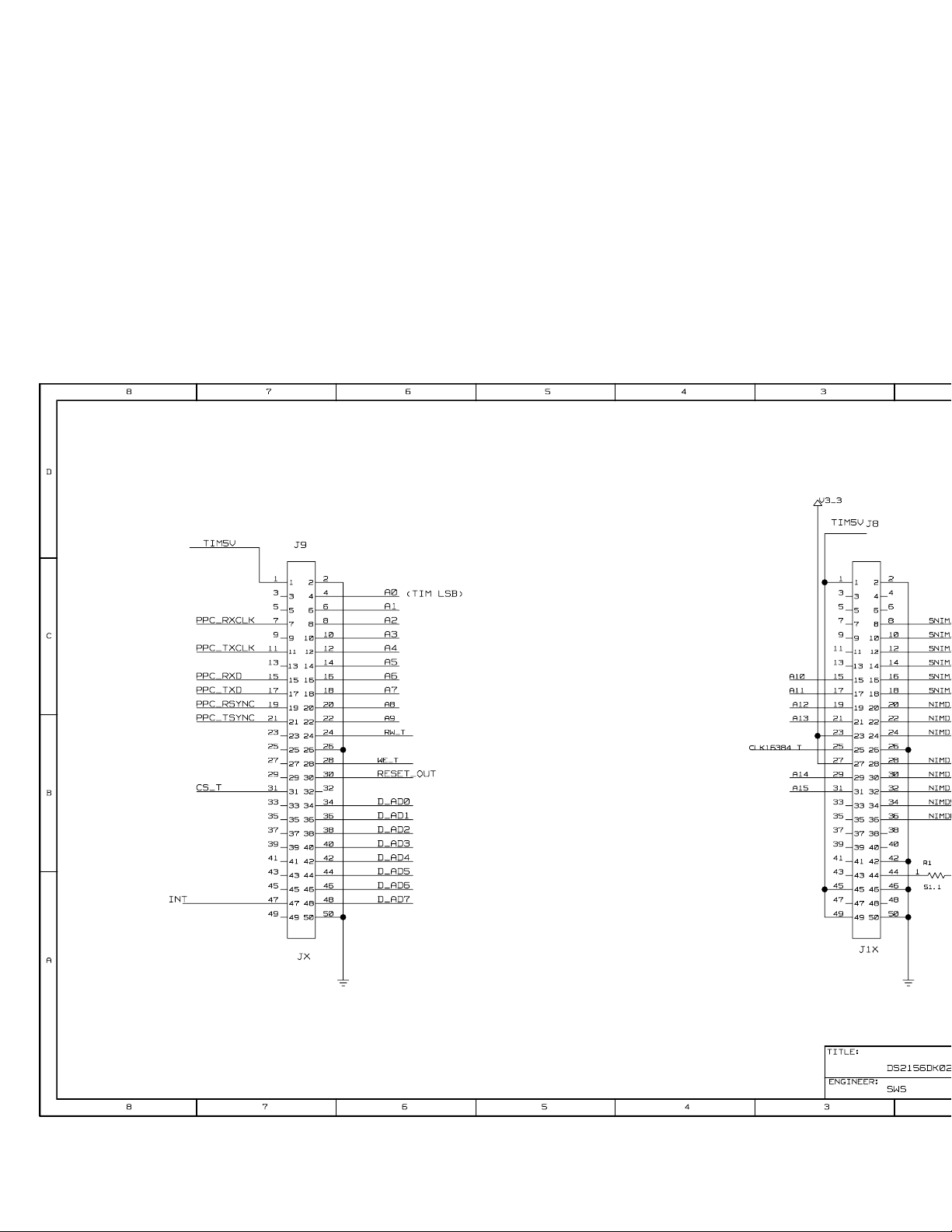
SCHEMATICS
The DS21354DK schematics are featured in the following 13 pages.
7 of 20


 Loading...