

查询DS21354L供应商
3.3V/5V E1 Single-Chip Transceivers
www.maxim-ic.com
GENERAL DESCRIPTION
The DS21354/DS213554 single-chip transceivers
(SCTs) contain all the necessary functions to connect to
E1 lines. The devices are upward-compatible versions
of the DS2153 and DS2154 SCTs. The on-board
clock/data recovery circuitry coverts the AMI/HDB3 E1
waveforms to an NRZ serial stream. Both devices
automatically adjust to E1 22AWG (0.6mm) twistedpair cables from 0 to over 2km in length. They can
generate the necessary G.703 waveshapes for both 75W
coax and 120W twisted cables. The on-board jitter
attenuator (selectable to either 32 bits or 128 bits) can
be placed in either the transmit or receive data paths.
The framer locates the frame and multiframe
boundaries and monitors the data stream for alarms. It is
also used for extracting and inserting signaling data, Si,
and Sa-bit information. The on-board HDLC controller
can be used for Sa-bit links or DS0s. The devices
contain a set of internal registers that the user can
access to control the operation of the units. Quick
access through the parallel control port allows a single
controller to handle many E1 lines. The devices fully
meet all the latest E1 specifications, including ITU-T
G.703, G.704, G.706, G.823, G.732, and I.431, ETS
300 011, 300 233, and 300 166, as well as CTR12 and
CTR4.
PIN CONFIGURATION
TOP VIEW
Dallas
Semiconductor
DS21354/DS21554
100
1
LQFP
DS21354/DS21554
FEATURES
§ Complete E1 (CEPT) PCM-30/ISDN-PRI
Transceiver Functionality
§ On-Board Long- and Short-Haul Line Interface
for Clock/Data Recovery and Waveshaping
§ 32-Bit or 128-Bit Crystal-Less Jitter Attenuator
§ Frames to FAS, CAS, CCS, and CRC4 Formats
§ Integral HDLC Controller with 64-Byte Buffers
Configurable for Sa Bits, DS0, or Sub-DS0
Operation
§ Dual Two-Frame Elastic Store Slip Buffers that
can Connect to Asynchronous Backplanes up to
8.192MHz
§ Interleaving PCM Bus Operation
§ 8-Bit Parallel Control Port that can be used
Directly on Either Multiplexed or
Nonmultiplexed Buses (Intel or Motorola)
§ Extracts and Inserts CAS Signaling
§ Detects and Generates Remote and AIS Alarms
§ Programmable Output Clocks for Fractional E1,
H0, and H12 Applications
§ Fully Independent Transmit and Receive
Functionality
§ Full Access to Si and Sa Bits Aligned with
CRC-4 Multiframe
§ Four Separate Loopback Functions for Testing
Functions
§ Large Counters for Bipolar and Code Violations,
CRC4 Codeword Errors, FAS Word Errors, and
E Bits
§ IEEE 1149.1 JTAG-Boundary Scan Architecture
§ Pin Compatible with DS2154/52/352/552 SCTs
§ 3.3V (DS21354) or 5V (DS21554) Supply; Low-
Power CMOS
§ 100-pin LQFP package (14mm x 14mm)
ORDERING INFORMATION
PART TEMP RANGE PIN-PACKAGE
DS21354L
DS21354LN -40°C to +85°C 100 LQFP
DS21554L
DS21554LN -40°C to +85°C 100 LQFP
0°C to +70°C 100 LQFP
0°C to +70°C 100 LQFP
Note: Some revisions of this device may incorporate deviations from published specifications known as errata. Multiple revisions of any device
may be simultaneously available through various sales channels. For information about device errata, click here: www.maxim-ic.com/errata
1 of 124
REV: 021004
.

DS21354/DS21554 3.3V/5V E1 Single-Chip Transceivers
TABLE OF CONTENTS
1. INTRODUCTION.................................................................................................................. 6
1.1. FUNCTIONAL DESCRIPTION..............................................................................................................................7
1.2. DOCUMENT REVISION HISTORY .............................................................................................................8
2. BLOCK DIAGRAM .............................................................................................................. 9
3. PIN DESCRIPTION............................................................................................................ 10
3.1. PIN FUNCTION DESCRIPTION ................................................................................................................14
3.1.1. Transmit-Side Pins ..............................................................................................................................14
3.1.2. Receive-Side Pins ...............................................................................................................................17
3.1.3. Parallel Control Port Pins ....................................................................................................................20
3.1.4. JTAG Test Access Port Pins...............................................................................................................22
3.1.5. Interleave Bus Operation Pins ............................................................................................................22
3.1.6. Line Interface Pins ..............................................................................................................................23
3.1.7. Supply Pins .........................................................................................................................................24
4. PARALLEL PORT............................................................................................................. 25
4.1. REGISTER MAP ........................................................................................................................................25
5. CONTROL, ID, AND TEST REGISTERS .......................................................................... 30
5.1. POWER-UP SEQUENCE ..........................................................................................................................30
5.2. SYNCHRONIZATION AND RESYNCHRONIZATION ...............................................................................32
5.3. FRAMER LOOPBACK ...............................................................................................................................36
5.4. AUTOMATIC ALARM GENERATION ........................................................................................................38
5.5. REMOTE LOOPBACK ...............................................................................................................................40
5.6. LOCAL LOOPBACK ...................................................................................................................................40
6. STATUS AND INFORMATION REGISTERS .................................................................... 43
6.1. CRC4 SYNC COUNTER............................................................................................................................45
7. ERROR COUNT REGISTERS........................................................................................... 50
7.1. BPV OR CODE VIOLATION COUNTER ...................................................................................................50
7.2. CRC4 ERROR COUNTER.........................................................................................................................51
7.3. E-BIT COUNTER .......................................................................................................................................51
7.4. FAS ERROR COUNTER .................................................................................................................................52
8. DS0 MONITORING FUNCTION ........................................................................................ 53
9. SIGNALING OPERATION................................................................................................. 56
9.1. PROCESSOR-BASED SIGNALING ..........................................................................................................56
9.2. HARDWARE-BASED SIGNALING ............................................................................................................58
9.2.1. Receive Side .......................................................................................................................................58
9.2.2. Transmit Side ......................................................................................................................................59
10. PER-CHANNEL CODE GENERATION AND LOOPBACK............................................... 60
10.1. TRANSMIT-SIDE CODE GENERATION ................................................................................................60
10.1.1. Simple Idle Code Insertion and Per-Channel Loopback .....................................................................60
10.1.2. Per-Channel Code Insertion ...............................................................................................................61
10.2. RECEIVE-SIDE CODE GENERATION...................................................................................................62
11. CLOCK BLOCKING REGISTERS..................................................................................... 63
2 of 124

DS21354/DS21554 3.3V/5V E1 Single-Chip Transceivers
12. ELASTIC STORES OPERATION...................................................................................... 65
12.1. RECEIVE SIDE .......................................................................................................................................65
12.2. TRANSMIT SIDE.....................................................................................................................................65
13. ADDITIONAL (SA) AND INTERNATIONAL (SI) BIT OPERATION.................................. 66
13.1. HARDWARE SCHEME ...........................................................................................................................66
13.2. INTERNAL REGISTER SCHEME BASED ON DOUBLE FRAME .........................................................66
13.3. INTERNAL REGISTER SCHEME BASED ON CRC4 MULTIFRAME....................................................68
14. HDLC CONTROLLER FOR THE SA BITS OR DS0 ......................................................... 70
14.1. GENERAL OVERVIEW...........................................................................................................................70
14.2. HDLC STATUS REGISTERS..................................................................................................................71
14.3. BASIC OPERATION DETAILS ...............................................................................................................72
14.3.1. Example: Receive an HDLC Message................................................................................................72
14.3.2. Example: Transmit an HDLC Message...............................................................................................72
14.4. HDLC REGISTER DESCRIPTION..........................................................................................................73
15. LINE INTERFACE FUNCTIONS........................................................................................ 80
15.1. RECEIVE CLOCK AND DATA RECOVERY.......................................................................................................81
15.2. TRANSMIT WAVESHAPING AND LINE DRIVING ..............................................................................................81
15.3. JITTER ATTENUATOR..................................................................................................................................82
15.4. PROTECTED INTERFACES ...........................................................................................................................86
15.5. RECEIVE MONITOR MODE ..........................................................................................................................89
16. JTAG BOUNDARY SCAN ARCHITECTURE AND TEST ACCESS PORT...................... 90
16.1. INSTRUCTION REGISTER.............................................................................................................................95
16.2. TEST REGISTERS.......................................................................................................................................96
17. INTERLEAVED PCM BUS OPERATION.......................................................................... 98
17.1. CHANNEL INTERLEAVE ...............................................................................................................................99
17.2. FRAME INTERLEAVE ...................................................................................................................................99
18. FUNCTIONAL TIMING DIAGRAMS................................................................................ 100
18.1. RECEIVE .................................................................................................................................................100
18.2. TRANSMIT ...............................................................................................................................................104
19. OPERATING PARAMETERS.......................................................................................... 111
20. AC TIMING PARAMETERS AND DIAGRAMS ............................................................... 112
20.1. MULTIPLEXED BUS AC CHARACTERISTICS ................................................................................................112
20.2. NONMULTIPLEXED BUS AC CHARACTERISTICS..........................................................................................115
20.3. RECEIVE-SIDE AC CHARACTERISTICS ......................................................................................................117
20.4. TRANSMIT AC CHARACTERISTICS.............................................................................................................121
21. PACKAGE INFORMATION............................................................................................. 124
3 of 124

DS21354/DS21554 3.3V/5V E1 Single-Chip Transceivers
LIST OF FIGURES
Figure 2-1. DS21354/554 Block Diagram ............................................................................................................................. 9
Figure 15-1. Basic External Analog Connections .............................................................................................................. 83
Figure 15-2. Optional Crystal Connection........................................................................................................................... 83
Figure 15-3. Jitter Tolerance................................................................................................................................................. 84
Figure 15-4. Jitter Attenuation .............................................................................................................................................. 84
Figure 15-5. Transmit Waveform Template ........................................................................................................................ 85
Figure 15-6. Protected Interface Example for the DS21554 ............................................................................................ 87
Figure 15-7. Protected Interface Example for the DS21354 ............................................................................................ 88
Figure 15-8. Typical Monitor Port Application .................................................................................................................... 89
Figure 16-1. JTAG Functional Block Diagram.................................................................................................................... 91
Figure 16-2. TAP Controller State Diagram ........................................................................................................................ 94
Figure 17-1. IBO Basic Configuration Using Four SCTs .................................................................................................. 99
Figure 18-1. Receive-Side Timing...................................................................................................................................... 100
Figure 18-2. Receive-Side Boundary Timing (with Elastic Store Disabled)................................................................. 100
Figure 18-3. Receive-Side 1.544MHz Boundary Timing (with Elastic Store Enabled) .............................................. 101
Figure 18-4. Receive-Side 2.048MHz Boundary Timing (with Elastic Store Enabled) .............................................. 101
Figure 18-5. Receive-Side Interleave Bus Operation, Byte Mode ................................................................................ 102
Figure 18-6. Receive-Side Interleave Bus Operation, Frame Mode ............................................................................. 103
Figure 18-7. Transmit-Side Timing .................................................................................................................................... 104
Figure 18-8. Transmit-Side Boundary Timing (with Elastic Store Disabled)................................................................ 104
Figure 18-9. Transmit-Side 1.544MHz Boundary Timing (with Elastic Store Enabled) ............................................. 105
Figure 18-10. Transmit-Side 2.048MHz Boundary Timing (with Elastic Store Enabled) ........................................... 105
Figure 18-11. Transmit-Side Interleave Bus Operation, Byte Mode ............................................................................. 106
Figure 18-12. Transmit-Side Interleave Bus Operation, Frame Mode.......................................................................... 107
Figure 18-13. G.802 Timing ................................................................................................................................................ 108
Figure 18-14. DS21354/DS21554 Framer Synchronization Flowchart ........................................................................ 109
Figure 18-15. DS21354/DS21554 Transmit Data Flow .................................................................................................. 110
Figure 20-1. Intel Bus Read Ac Timing (BTS = 0/MUX = 1)........................................................................................... 113
Figure 20-2. Intel Bus Write Timing (BTS = 0/MUX = 1)................................................................................................. 113
Figure 20-3. Motorola Bus AC Timing (BTS = 1/MUX = 1) ............................................................................................ 114
Figure 20-4. Intel Bus Read AC Timing (BTS = 0/MUX = 0).......................................................................................... 115
Figure 20-5. Intel Bus Write AC Timing (BTS = 0/MUX = 0) .......................................................................................... 116
Figure 20-6. Motorola Bus Read AC Timing (BTS = 1/MUX = 0).................................................................................. 116
Figure 20-7. Motorola Bus Write AC Timing (BTS = 1/MUX = 0) .................................................................................. 116
Figure 20-8. Receive-Side AC Timing ............................................................................................................................... 118
Figure 20-9. Receive System Side AC Timing................................................................................................................. 119
Figure 20-10. Receive Line Interface AC Timing............................................................................................................. 120
Figure 20-11. Transmit-Side AC Timing............................................................................................................................ 122
Figure 20-12. Transmit System Side AC Timing.............................................................................................................. 123
Figure 20-13. Transmit Line Interface Side AC Timing................................................................................................... 123
4 of 124

DS21354/DS21554 3.3V/5V E1 Single-Chip Transceivers
LIST OF TABLES
Table 3-1. Pin Description Sorted by Pin Number ............................................................................................................. 10
Table 3-2. Pin Description by Symbol ................................................................................................................................. 12
Table 4-1. Register Map Sorted by Address ...................................................................................................................... 25
Table 5-1. Device ID Bit Map ................................................................................................................................................ 30
Table 5-2. SYNC/RESYNC Criteria ..................................................................................................................................... 32
Table 6-1. Alarm Criteria ....................................................................................................................................................... 46
Table 14-1. HDLC Controller Register List ......................................................................................................................... 70
Table 15-1. Line Build-Out Select in LICR for the DS21554 ............................................................................................ 81
Table 15-2. Line Build-Out Select in LICR for the DS21354 ............................................................................................ 82
Table 15-3. Transformer Specifications .............................................................................................................................. 82
Table 15-4. Receive Monitor Mode Gain ............................................................................................................................ 89
Table 16-1. Instruction Codes for IEEE 1149.1 Architecture ........................................................................................... 95
Table 16-2. ID Code Structure.............................................................................................................................................. 96
Table 16-3. Device ID Codes................................................................................................................................................ 96
Table 16-4. Boundary Scan Control Bits............................................................................................................................. 97
Table 17-1. IBO Master Device Select ................................................................................................................................98
5 of 124
DS21354/DS21554 3.3V/5V E1 Single-Chip Transceivers
1. INTRODUCTION
The DS21354/DS21554 are superset versions of the popular DS2153 and DS2154 SCTs offering the new
features listed below. All the original features of the DS2153 and DS2154 have been retained, and the
software created for the original devices is transferable into the DS21354/DS21554.
New Features in the DS21354 and DS21554
FEATURE SECTION
HDLC controller with 64-Byte Buffers for Sa Bits or DS0s or Sub DS0s 14
Interleaving PCM Bus Operation 17
IEEE 1149.1 JTAG-Boundary Scan Architecture 16
3.3V (DS21354 Only) Supply 1.1 and 2
Line Interface Support for the G.703 2.048 Synchronization Interface 15
Customer Disconnect Indication (...101010...) Generator 5.6
Open-Drain Line Driver Option 5.6
Additional Features in the DS21354 and DS21554
FEATURE SECTION
Option for nonmultiplexed bus operation 1.1 and 20.2
Crystal-less jitter attenuation 15.3
Additional hardware signaling capability including:
Receive signaling reinsertion to a backplane multiframe sync
Availability of signaling in a separate PCM data stream
Signaling freezing Interrupt generated on change of signaling data
Improved receive sensitivity: 0 to -43dB 1.1
Per-channel code insertion in both transmit and receive paths 10
Expanded access to Sa and Si bits 13
RCL, RLOS, RRA, and RAIS alarms now interrupt on change of state 6
8.192MHz clock synthesizer 1.1
Per-channel loopback 10
Addition of hardware pins to indicate carrier loss and signaling freeze 1.1
Line interface function can be completely decoupled from the framer/formatter to
allow:
Interface to optical, HDSL, and other NRZ interfaces
“tap” the transmit and receive bipolar data streams for monitoring purposes
Be able to corrupt data and insert framing errors, CRC errors, etc.
Transmit and receive elastic stores now have independent backplane clocks 1.1
Ability to monitor one DS0 channel in both the transmit and receive paths 8
Access to the data streams in between the framer/formatter and the elastic stores 1.1
AIS generation in the line interface that is independent of loopbacks 1.1 and 5
Transmit current limiter to meet the 50mA short circuit requirement 15
Option to extend carrier loss criteria to a 1ms period as per ETS 300 233 5.4
Automatic RAI generation to ETS 300 011 specifications 5.4
9
1.1
6 of 124

DS21354/DS21554 3.3V/5V E1 Single-Chip Transceivers
1.1. Functional Description
The analog AMI/HDB3 waveform off the E1 line is transformer coupled into the RRING and RTIP pins
of the DS21354/554. The device recovers clock and data from the analog signal and passes it through the
jitter attenuation mux to the receive-side framer where the digital serial stream is analyzed to locate the
framing/multiframe pattern. The DS21354/DS21554 contain an active filter that reconstructs the analogreceived signal for the nonlinear losses that occur in transmission. The devices have a usable receive
sensitivity of 0 to -43dB, which allows the device to operate on cables over 2km in length. The receiveside framer locates FAS frame and CRC and CAS multiframe boundaries as well as detects incoming
alarms including, carrier loss, loss of synchronization, AIS, and Remote Alarm. If needed, the receiveside elastic store can be enabled to absorb the phase and frequency differences between the recovered E1
data stream and an asynchronous backplane clock, which is provided at the RSYSCLK input. The clock
applied at the RSYSCLK input can be either a 2.048MHz/4.096MHz/8.192MHz clock or a 1.544MHz
clock.
The transmit-side framer is totally independent from the receive side in both the clock requirements and
characteristics. Data off a backplane can be passed through a transmit-side elastic store if necessary. The
transmit formatter provides the necessary frame/multiframe data overhead for E1 transmission.
Reader’s Note: This data sheet assumes a particular nomenclature of the E1 operating environment. In
each 125ms frame, there are 32 eight-bit time slots numbered 0 to 31. Time slot 0 is transmitted first and
received first. These 32 time slots are also referred to as channels with a numbering scheme of 1 to 32.
Time slot 0 is identical to channel 1, time slot 1 is identical to Channel 2, and so on. Each time slot (or
channel) is made up of eight bits, which are numbered 1 to 8. Bit number 1 is the most significant bit
(MSB) and is transmitted first. Bit number 8 is the least significant bit (LSB) and is transmitted last. The
term “locked” refers to two clock signals that are phase or frequency locked, or derived from a common
clock (i.e., a 1.544MHz clock may be locked to a 2.048MHz clock if they share the same 8kHz
component). Throughout this data sheet, the following abbreviations are used:
NAME FUNCTION
FAS Frame-Alignment Signal
CAS Channel-Associated Signaling
MF Multiframe
Si International Bits
CRC4 Cyclical Redundancy Check
CCS Common-Channel Signaling
Sa Additional Bits
E-Bit CRC4 Error Bits
7 of 124

DS21354/DS21554 3.3V/5V E1 Single-Chip Transceivers
1.2. Document Revision History
REVISION DESCRIPTION
012799 Initial release
012899
Corrected TSYSCLK and RSYSCLK timing and added 4.096MHz and 8.192MHz
timing
020399 Corrected definition and label of TUDR bit in the THIR register.
021199 Corrected address of IBO register in text.
040199 Added Receive Monitor Mode section
041599 Added section on Protected Interfaces
050799 Corrected pin number and description of FMS in JTAG section
072999 Added list of tables and figures
091499
092399
Added 10mF cap to interface examples
Corrected definition of DS in pin description.
072401 Typo corrected in JTAG Test Access Port Pins.
Added note to the Receive Information Register, FAS Resync Criteria Met.
Corrected Figures 20-1, 20-2, 20-3 with respect to CS.
021004
Corrected typo in Figure 18-14 (RCR1.1 reference corrected).
Corrected formatting issues.
8 of 124
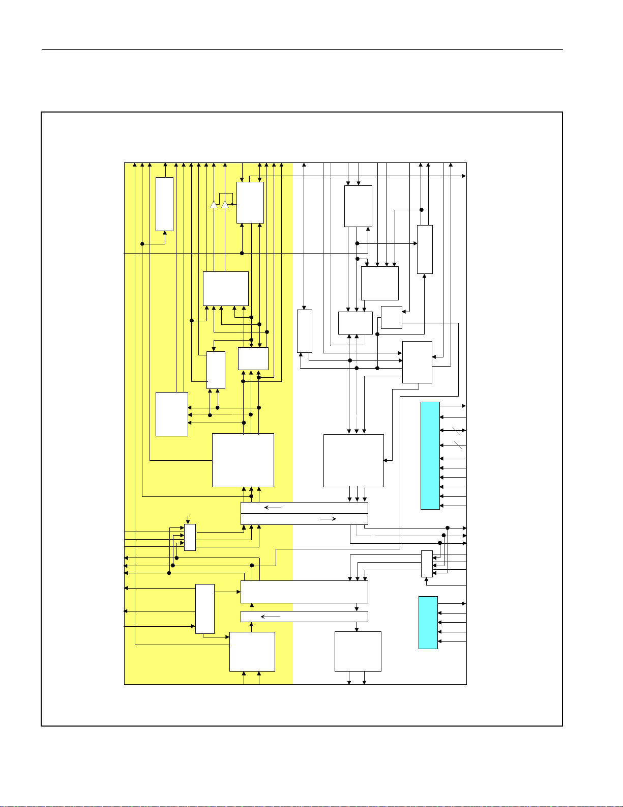
2. BLOCK DIAGRAM
/
Figure 2-1. DS21354/554 Block Diagram
RSIGF
RCHCLK
RCHBLK
RLINK
RLOS/LOTC
RCL
RCLK
RLCLK
8MCLK
Synthesizer
8.192MHz Clock
RSER
RSYSCLK
RSIG
RSYNC
Interleave
Bus
RMSYNC
RFSYNC
DS21354/DS21554 3.3V/5V E1 Single-Chip Transceivers
RDATA
TESO
TDATA
TSYNC
TSSYNC
Interleave
TSIG
TSYSCLK
TSER
Bus
TCHBLK
TLINK
TCLK
TLCLK
TCHCLK
CO
RPOSI
RCLKI
RNEGI
RNEGO
RCLKO
RPOSO
8XCLK
XTALD
MCLK
Buffer
Signaling
Control
Framer
Receive Side
32.768MHz
Clock / Data
Reco very
RSYSCLK
Store
Elastic
DS21354
DS21554
DATA
SYNC
CLOCK
Framer Loopback
Remote Loopback
Jitter Attenuator
Either transmit or receive path
Local Loopback
Receive
Line I/F
Timing Control
Hardware
Signaling
Insertion
LOTC
Store
Elastic
Sync Control
SYNC
CLOCK
Formatter
Transmit Side
r
T
i
m
s
t
n
a
L
I
i
e
/
n
F
MUX
HDLC/BOC
Controller
Sa / DS0
INT*
Sa
DATA
(routed to all blocks)
Parallel & Test Control Port
MUX
JTAG PORT
MUX
D0 to D7 /
AD0 to AD7
8
A0 to A6
7
ALE(AS) / A7
RD*(DS*)
WR*(R/W*)
BTS
CS*
TEST
TPOSO
TCLKO
TNEGO
TNEGI
TCLKI
TPOSI
LIUC
JTDO
JTDI
JTCLK
JTMS
J
S
R
*
T
CI
Timing
HDLC/BOC
Controller
Sa / DS0
LIUC
MUX
16.384 MH z
VCO / PLL
RTIP
RRING
TTIP
TRING
9 of 124

DS21354/DS21554 3.3V/5V E1 Single-Chip Transceivers
3. PIN DESCRIPTION
Table 3-1. Pin Description Sorted by Pin Number
PIN NAME TYPE FUNCTION
1 RCHBLK O Receive Channel Block
2 JTMS I IEEE 1149.1 Test Mode Select
3 8MCLK O 8.192 MHz Clock
4 JTCLK I IEEE 1149.1 Test Clock Signal
5
JTRST
6 RCL O Receive Carrier Loss
7 JTDI I IEEE 1149.1 Test Data Input
8, 9, 15,
23, 26, 27,
N.C. — No Connect. Do not connect any signal to this pin.
28
10 JTDO O IEEE 1149.1 Test Data Output
11 BTS I Bus Type Select
12 LIUC I Line Interface Connect
13 8XCLK O Eight Times Clock
14 TEST I Test
16 RTIP I Receive Analog Tip Input
17 RRING I Receive Analog Ring Input
18 RVDD – Receive Analog Positive Supply
19, 20, 24 RVSS – Receive Analog Signal Ground
21 MCLK I Master Clock Input
22 XTALD O Quartz Crystal Driver
25
INT
29 TTIP O Transmit Analog Tip Output
30 TVSS – Transmit Analog Signal Ground
31 TVDD – Transmit Analog Positive Supply
32 TRING O Transmit Analog Ring Output
33 TCHBLK O Transmit Channel Block
34 TLCLK O Transmit Link Clock
35 TLINK I Transmit Link Data
36 CI I Carry In
37 TSYNC I/O Transmit Sync
38 TPOSI I Transmit Positive Data Input
39 TNEGI I Transmit Negative Data Input
40 TCLKI I Transmit Clock Input
41 TCLKO O Transmit Clock Output
42 TNEGO O Transmit Negative Data Output
43 TPOSO O Transmit Positive Data Output
44, 61,
81,83
45, 60, 80,
84
DVDD — Digital Positive Supply
DVSS — Digital Signal Ground
46 TCLK I Transmit Clock
47 TSER I Transmit Serial Data
48 TSIG I Transmit Signaling Input
I IEEE 1149.1 Test Reset, Active Low
O Interrupt, Active Low
10 of 124

DS21354/DS21554 3.3V/5V E1 Single-Chip Transceivers
PIN NAME TYPE FUNCTION
49 TESO O Transmit Elastic Store Output
50 TDATA I Transmit Data
51 TSYSCLK I Transmit System Clock
52 TSSYNC I Transmit System Sync
53 TCHCLK O Transmit Channel Clock
54 CO O Carry Out
55 MUX I Bus Operation
56 D0/AD0 I/O Data Bus Bit0/Address/Data Bus Bit 0
57 D1/AD1 I/O Data Bus Bit1/Address/Data Bus Bit 1
58 D2/AD2 I/O Data Bus Bit 2/Address/Data Bus 2
59 D3/AD3 I/O Data Bus Bit 3/Address/Data Bus Bit 3
62 D4/AD4 I/O Data Bus Bit4/Address/Data Bus Bit 4
63 D5/AD5 I/O Data Bus Bit 5/Address/Data Bus Bit 5
64 D6/AD6 I/O Data Bus Bit 6/Address/Data Bus Bit 6
65 D7/AD7 I/O Data Bus Bit 7/Address/Data Bus Bit 7
66 A0 I Address Bus Bit 0
67 A1 I Address Bus Bit 1
68 A2 I Address Bus Bit 2
69 A3 I Address Bus Bit 3
70 A4 I Address Bus Bit 4
71 A5 I Address Bus Bit 5
72 A6 I Address Bus Bit 6
73 ALE (AS)/A7 I Address Latch Enable/Address Bus Bit 7
74
75
76
77
RD (DS)
CS
FMS
WR (R/W)
I Read Input (Data Strobe), Active Low
I Chip Select, Active Low
I Framer Mode Select
I Write Input (Read/Write), Active Low
78 RLINK O Receive Link Data
79 RLCLK O Receive Link Clock
82 RCLK O Receive Clock
85 RDATA O Receive Data
86 RPOSI I Receive Positive Data Input
87 RNEGI I Receive Negative Data Input
88 RCLKI I Receive Clock Input
89 RCLKO O Receive Clock Output
90 RNEGO O Receive Negative Data Output
91 RPOSO O Receive Positive Data Output
92 RCHCLK O Receive Channel Clock
93 RSIGF O Receive Signaling Freeze Output
94 RSIG O Receive Signaling Output
95 RSER O Receive Serial Data
96 RMSYNC O Receive Multiframe Sync
97 RFSYNC O Receive Frame Sync
98 RSYNC I/O Receive Sync
99 RLOS/LOTC O Receive Loss Of Sync/ Loss Of Transmit Clock
100 RSYSCLK I Receive System Clock
11 of 124

DS21354/DS21554 3.3V/5V E1 Single-Chip Transceivers
Table 3-2. Pin Description by Symbol
PIN NAME TYPE FUNCTION
3 8MCLK O 8.192MHz Clock
13 8XCLK O Eight-Times Clock
66 A0 I Address Bus Bit 0
67 A1 I Address Bus Bit 1
68 A2 I Address Bus Bit 2
69 A3 I Address Bus Bit 3
70 A4 I Address Bus Bit 4
71 A5 I Address Bus Bit 5
72 A6 I Address Bus Bit 6
73 ALE (AS)/A7 I Address Latch Enable/Address Bus Bit 7
11 BTS I Bus Type Select
36 CI I Carry In
54 CO O Carry Out
75
CS
56 D0/AD0 I/O Data Bus Bit0/ Address/Data Bus Bit 0
57 D1/AD1 I/O Data Bus Bit1/ Address/Data Bus Bit 1
58 D2/AD2 I/O Data Bus Bit 2/Address/Data Bus 2
59 D3/AD3 I/O Data Bus Bit 3/Address/Data Bus Bit 3
62 D4/AD4 I/O Data Bus Bit4/Address/Data Bus Bit 4
63 D5/AD5 I/O Data Bus Bit 5/Address/Data Bus Bit 5
64 D6/AD6 I/O Data Bus Bit 6/Address/Data Bus Bit 6
65 D7/AD7 I/O Data Bus Bit 7/Address/Data Bus Bit 7
44, 61, 81, 83 DVDD — Digital Positive Supply
45, 60, 80, 84 DVSS — Digital Signal Ground
76 FMS I Framer Mode Select
25
INT
4 JTCLK I IEEE 1149.1 Test Clock Signal
7 JTDI I IEEE 1149.1 Test Data Input
10 JTDO O IEEE 1149.1 Test Data Output
2 JTMS I IEEE 1149.1 Test Mode Select
5
JTRST
12 LIUC I Line Interface Connect
21 MCLK I Master Clock Input
55 MUX I Bus Operation
8, 9, 15, 23, 26,
27, 28
N.C. — No Connect. Do not connect any signal to this pin.
1 RCHBLK O Receive Channel Block
92 RCHCLK O Receive Channel Clock
6 RCL O Receive Carrier Loss
82 RCLK O Receive Clock
88 RCLKI I Receive Clock Input
89 RCLKO O Receive Clock Output
74
RD (DS)
85 RDATA O Receive Data
97 RFSYNC O Receive Frame Sync
79 RLCLK O Receive Link Clock
I Chip Select, Active Low
O Interrupt
I IEEE 1149.1 Test Reset, Active Low
I Read Input (Data Strobe), Active Low
12 of 124

DS21354/DS21554 3.3V/5V E1 Single-Chip Transceivers
PIN NAME TYPE FUNCTION
78 RLINK O Receive Link Data
99 RLOS/LOTC O Receive Loss of Sync/Loss of Transmit Clock
96 RMSYNC O Receive Multiframe Sync
87 RNEGI I Receive Negative Data Input
90 RNEGO O Receive Negative Data Output
86 RPOSI I Receive Positive Data Input
91 RPOSO O Receive Positive Data Output
17 RRING I Receive Analog Ring Input
95 RSER O Receive Serial Data
94 RSIG O Receive Signaling Output
93 RSIGF O Receive Signaling Freeze Output
98 RSYNC I/O Receive Sync
100 RSYSCLK I Receive System Clock
16 RTIP I Receive Analog Tip Input
18 RVDD — Receive Analog Positive Supply
19, 20, 24 RVSS — Receive Analog Signal Ground
33 TCHBLK O Transmit Channel Block
53 TCHCLK O Transmit Channel Clock
46 TCLK I Transmit Clock
40 TCLKI I Transmit Clock Input
41 TCLKO O Transmit Clock Output
50 TDATA I Transmit Data
49 TESO O Transmit Elastic Store Output
14 TEST I Test
34 TLCLK O Transmit Link Clock
35 TLINK I Transmit Link Data
39 TNEGI I Transmit Negative Data Input
42 TNEGO O Transmit Negative Data Output
38 TPOSI I Transmit Positive Data Input
43 TPOSO O Transmit Positive Data Output
32 TRING O Transmit Analog Ring Output
47 TSER I Transmit Serial Data
48 TSIG I Transmit Signaling Input
52 TSSYNC I Transmit System Sync
37 TSYNC I/O Transmit Sync
51 TSYSCLK I Transmit System Clock
29 TTIP O Transmit Analog Tip Output
31 TVDD — Transmit Analog Positive Supply
30 TVSS — Transmit Analog Signal Ground
77
WR (R/W)
I Write Input (Read/Write), Active Low
22 XTALD O Quartz Crystal Driver
13 of 124

DS21354/DS21554 3.3V/5V E1 Single-Chip Transceivers
3.1. Pin Function Description
3.1.1. Transmit-Side Pins
Signal Name:
Signal Description:
Signal Type:
TCLK
Transmit Clock
Input
A 2.048MHz primary clock. Used to clock data through the transmit side formatter.
Signal Name:
Signal Description:
Signal Type:
TSER
Transmit Serial Data
Input
Transmit NRZ serial data. Sampled on the falling edge of TCLK when the transmit side elastic store is
disabled. Sampled on the falling edge of TSYSCLK when the transmit side elastic store is enabled.
Signal Name:
Signal Description:
Signal Type:
TCHCLK
Transmit Channel Clock
Output
A 256kHz clock that pulses high during the LSB of each channel. Synchronous with TCLK when the
transmit side elastic store is disabled. Synchronous with TSYSCLK when the transmit side elastic store is
enabled. Useful for parallel to serial conversion of channel data.
Signal Name:
Signal Description:
Signal Type:
TCHBLK
Transmit Channel Block
Output
A user-programmable output that can be forced high or low during any of the 32 E1 channels.
Synchronous with TCLK when the transmit side elastic store is disabled. Synchronous with TSYSCLK
when the transmit-side elastic store is enabled. Useful for blocking clocks to a serial UART or LAPD
controller in applications where not all E1 channels are used such as Fractional E1, 384kbps (H0),
768kbps, or ISDN–PRI. Also useful for locating individual channels in drop-and-insert applications, for
external per-channel loopback, and for per-channel conditioning. See Section 12 for details.
Signal Name:
Signal Description:
Signal Type:
TSYSCLK
Transmit System Clock
Input
1.544MHz, 2.048MHz, 4.096MHz, or 8.192MHz clock. Only used when the transmit-side elastic store
function is enabled. Should be tied low in applications that do not use the transmit-side elastic store. See
Section 17
for details on 4.096MHz and 8.192MHz operation using the Interleave Bus Option.
Signal Name:
Signal Description:
Signal Type:
TLCLK
Transmit Link Clock
Output
4kHz to 20kHz demand clock (Sa bits) for the TLINK input. See Section 17 for details.
14 of 124

DS21354/DS21554 3.3V/5V E1 Single-Chip Transceivers
Signal Name:
Signal Description:
Signal Type:
TLINK
Transmit Link Data
Input
If enabled, this pin will be sampled on the falling edge of TCLK for data insertion into any combination
of the Sa bit positions (Sa4 to Sa8). See Section 13 for details.
Signal Name:
Signal Description:
Signal Type:
TSYNC
Transmit Sync
Input/Output
A pulse at this pin will establish either frame or multiframe boundaries for the transmit side. Via TCR1.1,
the DS21354/DS21554 can be programmed to output either a frame or multiframe pulse at this pin. This
pin can also be configured as an input via TCR1.0. See Section 18 for details.
Signal Name:
Signal Description:
Signal Type:
TSSYNC
Transmit System Sync
Input
Only used when the transmit-side elastic store is enabled. A pulse at this pin will establish either frame or
multiframe boundaries for the transmit side. Should be tied low in applications that do not use the
transmit-side elastic store.
Signal Name:
Signal Description:
Signal Type:
TSIG
Transmit Signaling Input
Input
When enabled, this input will sample signaling bits for insertion into outgoing PCM E1 data stream.
Sampled on the falling edge of TCLK when the transmit-side elastic store is disabled. Sampled on the
falling edge of TSYSCLK when the transmit-side elastic store is enabled.
Signal Name:
Signal Description:
Signal Type:
TESO
Transmit Elastic Store Data Output
Output
Updated on the rising edge of TCLK with data out of the transmit-side elastic store whether the elastic
store is enabled or not. This pin is normally tied to TDATA.
Signal Name:
Signal Description:
Signal Type:
TDATA
Transmit Data
Input
Sampled on the falling edge of TCLK with data to be clocked through the transmit-side formatter. This
pin is normally tied to TESO.
Signal Name:
Signal Description:
Signal Type:
TPOSO
Transmit Positive Data Output
Output
Updated on the rising edge of TCLKO with the bipolar data out of the transmit-side formatter. Can be
programmed to source NRZ data via the Output Data Format (TCR2.2) control bit. This pin is normally
tied to TPOSI.
15 of 124

DS21354/DS21554 3.3V/5V E1 Single-Chip Transceivers
Signal Name:
Signal Description:
Signal Type:
TNEGO
Transmit Negative Data Output
Output
Updated on the rising edge of TCLKO with the bipolar data out of the transmit-side formatter. This pin is
normally tied to TNEGI.
Signal Name:
Signal Description:
Signal Type:
TCLKO
Transmit Clock Output
Output
Buffered output of signal that is clocking data through the transmit-side formatter. This pin is normally
tied to TCLKI.
Signal Name:
Signal Description:
Signal Type:
TPOSI
Transmit Positive Data Input
Input
Sampled on the falling edge of TCLKI for data to be transmitted out onto the T1 line. Can be internally
connected to TPOSO by tying the LIUC pin high. TPOSI and TNEGI can be tied together in NRZ
applications.
Signal Name:
Signal Description:
Signal Type:
TNEGI
Transmit Negative Data Input
Input
Sampled on the falling edge of TCLKI for data to be transmitted out onto the T1 line. Can be internally
connected to TNEGO by tying the LIUC pin high. TPOSI and TNEGI can be tied together in NRZ
applications.
Signal Name:
Signal Description:
Signal Type:
TCLKI
Transmit Clock Input
Input
Line interface transmit clock. Can be internally connected to TCLKO by tying the LIUC pin high.
16 of 124

DS21354/DS21554 3.3V/5V E1 Single-Chip Transceivers
3.1.2. Receive-Side Pins
Signal Name:
Signal Description:
Signal Type:
RLINK
Receive Link Data
Output
Updated with the fully recovered E1 data stream on the rising edge of RCLK.
Signal Name:
Signal Description:
Signal Type:
RLCLK
Receive Link Clock
Output
4kHz to 20kHz clock (Sa bits) for the RLINK output. See Section 13 for details.
Signal Name:
Signal Description:
Signal Type:
RCLK
Receive Clock
Output
2.048MHz clock that is used to clock data through the receive-side framer.
Signal Name:
Signal Description:
Signal Type:
RCHCLK
Receive Channel Clock
Output
A 256kHz clock that pulses high during the LSB of each channel. Synchronous with RCLK when the
receive-side elastic store is disabled. Synchronous with RSYSCLK when the receive-side elastic store is
enabled. Useful for parallel to serial conversion of channel data.
Signal Name:
Signal Description:
Signal Type:
RCHBLK
Receive Channel Block
Output
A user-programmable output that can be forced high or low during any of the 32 E1 channels.
Synchronous with RCLK when the receive-side elastic store is disabled. Synchronous with RSYSCLK
when the receive-side elastic store is enabled. Useful for blocking clocks to a serial UART or LAPD
controller in applications where not all E1 channels are used such as Fractional E1, 384kbps service,
768kbps, or ISDN–PRI. Also useful for locating individual channels in drop-and-insert applications, for
external per-channel loopback, and for per-channel conditioning. See Section 10 for details.
Signal Name:
Signal Description:
Signal Type:
RSER
Receive Serial Data
Output
Received NRZ serial data. Updated on rising edges of RCLK when the receive-side elastic store is
disabled. Updated on the rising edges of RSYSCLK when the receive-side elastic store is enabled.
Signal Name:
Signal Description:
Signal Type:
RSYNC
Receive Sync
Input/Output
An extracted pulse, one RCLK wide, is output at this pin that identifies either frame or CAS/CRC
multiframe boundaries. If the receive-side elastic store is enabled, then this pin can be enabled to be an
input at which a frame or multiframe boundary pulse synchronous with RSYSCLK is applied.
17 of 124

DS21354/DS21554 3.3V/5V E1 Single-Chip Transceivers
Signal Name:
Signal Description:
Signal Type:
RFSYNC
Receive Frame Sync
Output
An extracted 8kHz pulse, one RCLK wide, is output at this pin that identifies frame boundaries.
Signal Name:
Signal Description:
Signal Type:
RMSYNC
Receive Multiframe Sync
Output
If the receive-side elastic store is enabled, an extracted pulse, one RSYSCLK wide, is output at this pin
that identifies multiframe boundaries. If the receive-side elastic store is disabled, then this output will
output multiframe boundaries associated with RCLK.
Signal Name:
Signal Description:
Signal Type:
RDATA
Receive Data
Output
Updated on the rising edge of RCLK with the data out of the receive-side framer.
Signal Name:
Signal Description:
Signal Type:
RSYSCLK
Receive System Clock
Input
1.544MHz, 2.048MHz, 4.096MHz, or 8.192MHz clock. Only used when the receive-side elastic store
function is enabled. Should be tied low in applications that do not use the receive-side elastic store. See
Section 17 for details on 4.096MHz and 8.192MHz operation using the Interleave Bus Option.
Signal Name:
Signal Description:
Signal Type:
RSIG
Receive Signaling Output
Output
Outputs signaling bits in a PCM format. Updated on rising edges of RCLK when the receive-side elastic
store is disabled. Updated on the rising edges of RSYSCLK when the receive-side elastic store is enabled.
Signal Name:
Signal Description:
Signal Type:
RLOS/LOTC
Receive Loss of Sync / Loss of Transmit Clock
Output
A dual function output that is controlled by the TCR2.0 control bit. This pin can be programmed to either
toggle high when the synchronizer is searching for the frame and multiframe or to toggle high if the
TCLK pin has not been toggled for 5ms.
Signal Name:
Signal Description:
Signal Type:
RCL
Receive Carrier Loss
Output
Set high when the line interface detects a carrier loss.
Signal Name:
Signal Description:
Signal Type:
RSIGF
Receive Signaling Freeze
Output
Set high when the signaling data is frozen via either automatic or manual intervention. Used to alert
downstream equipment of the condition.
18 of 124

DS21354/DS21554 3.3V/5V E1 Single-Chip Transceivers
Signal Name:
Signal Description:
Signal Type:
8MCLK
8MHz Clock
Output
An 8.192MHz clock output that is referenced to the clock that is output at the RCLK pin.
Signal Name:
Signal Description:
Signal Type:
RPOSO
Receive Positive Data Input
Output
Updated on the rising edge of RCLKO with bipolar data out of the line interface. This pin is normally tied
to RPOSI.
Signal Name:
Signal Description:
Signal Type:
RNEGO
Receive Negative Data Input
Output
Updated on the rising edge of RCLKO with the bipolar data out of the line interface. This pin is normally
tied to RNEGI.
Signal Name:
Signal Description:
Signal Type:
RCLKO
Receive Clock Output
Output
Buffered recovered clock from the T1 line. This pin is normally tied to RCLKI.
Signal Name:
Signal Description:
Signal Type:
RPOSI
Receive Positive Data Input
Input
Sampled on the falling edge of RCLKI for data to be clocked through the receive-side framer. RPOSI and
RNEGI can be tied together for a NRZ interface. Can be internally connected to RPOSO by tying the
LIUC pin high.
Signal Name:
Signal Description:
Signal Type:
RNEGI
Receive Negative Data Input
Input
Sampled on the falling edge of RCLKI for data to be clocked through the receive-side framer. RPOSI and
RNEGI can be tied together for a NRZ interface. Can be internally connected to RNEGO by tying the
LIUC pin high.
Signal Name:
Signal Description:
Signal Type:
RCLKI
Receive Clock Input
Input
Clock used to clock data through the receive-side framer. This pin is normally tied to RCLKO. Can be
internally connected to RCLKO by tying the LIUC pin high.
19 of 124

DS21354/DS21554 3.3V/5V E1 Single-Chip Transceivers
3.1.3. Parallel Control Port Pins
Signal Name:
Signal Description:
Signal Type:
INT
Interrupt
Output
Active-low, open-drain output that flags host controller during conditions and change of conditions
defined in the Status Registers 1 and 2 and the HDLC Status Register.
Signal Name:
Signal Description:
Signal Type:
FMS
Framer Mode Select
Input
Selects the DS2154 mode when high or the DS21354/DS21554 mode when low. If high, the JTRST is
internally pulled low. If low, JTRST has normal JTAG functionality. This pin has a 10kW pullup resistor.
Signal Name:
Signal Description:
Signal Type:
TEST
Tri-State Control
Input
Set high to tri-state all output and I/O pins (including the parallel control port). Set low for normal
operation. Useful in board-level testing.
Signal Name:
Signal Description:
Signal Type:
MUX
Bus Operation
Input
Set low to select nonmultiplexed bus operation. Set high to select multiplexed bus operation.
Signal Name:
Signal Description:
Signal Type:
AD0 to AD7
Data Bus [D0 to D7] or Address/Data Bus
Input
In nonmultiplexed bus operation (MUX = 0), serves as the data bus. In multiplexed bus operation
(MUX = 1), serves as an 8-bit multiplexed address/data bus.
Signal Name:
Signal Description:
Signal Type:
A0 to A6
Address Bus
Input
In nonmultiplexed bus operation (MUX = 0), serves as the address bus. In multiplexed bus operation
(MUX = 1), these pins are not used and should be tied low.
Signal Name:
Signal Description:
Signal Type:
BTS
Bus Type Select
Input
Strap high to select Motorola bus timing; strap low to select Intel bus timing. This pin controls the
function of the RD (DS), ALE (AS), and WR (R/W) pins. If BTS = 1, then these pins assume the function
listed in parentheses ().
20 of 124

DS21354/DS21554 3.3V/5V E1 Single-Chip Transceivers
Signal Name:
Signal Description:
Signal Type:
RD (DS)
Read Input—Data Strobe
Input
In Intel Mode, RD determines when data is read from the device. In Motorola Mode, DS is used to write
to the device. See the Bus Timing Diagrams section.
Signal Name:
Signal Description:
Signal Type:
CS
Chip Select
Input
Must be low to read or write to the device. CS is an active-low signal.
Signal Name:
Signal Description:
Signal Type:
ALE (AS)/A7
Address Latch Enable (Address Strobe) or A7
Input
In nonmultiplexed bus operation (MUX = 0), serves as the upper address bit. In multiplexed bus
operation (MUX = 1), serves to demultiplex the bus on a positive-going edge.
Signal Name:
Signal Description:
Signal Type:
WR (R/W)
Write Input (Read/Write)
Input
WR is an active-low signal.
21 of 124

DS21354/DS21554 3.3V/5V E1 Single-Chip Transceivers
3.1.4. JTAG Test Access Port Pins
Signal Name:
Signal Description:
Signal Type:
JTRST
IEEE 1149.1 Test Reset
Input
This signal is used to asynchronously reset the test access port controller. At power up, JTRST must be
toggled from low to high. This action will set the device into JTAG DEVICE ID mode enabling the test
access port features. This pin has a 10kW pullup resistor. When FMS = 1, this pin is tied low internally.
Tie JTRST low if JTAG is not used and the framer is in DS21354/DS21554 mode (FMS low).
Signal Name:
Signal Description:
Signal Type:
JTMS
IEEE 1149.1 Test Mode Select
Input
This pin is sampled on the rising edge of JTCLK and is used to place the test access port into the various
defined IEEE 1149.1 states. This pin has a 10kW pullup resistor.
Signal Name:
Signal Description:
Signal Type:
JTCLK
IEEE 1149.1 Test Clock Signal
Input
This signal is used to shift data into JTDI on the rising edge and out of JTDO on the falling edge.
Signal Name:
Signal Description:
Signal Type:
JTDI
IEEE 1149.1 Test Data Input
Input
Test instructions and data are clocked into this pin on the rising edge of JTCLK. This pin has a 10kW
pullup resistor.
Signal Name:
Signal Description:
Signal Type:
JTDO
IEEE 1149.1 Test Data Output
Output
Test instructions and data are clocked out of this pin on the falling edge of JTCLK. If not used, this pin
should be left unconnected.
3.1.5. Interleave Bus Operation Pins
Signal Name:
Signal Description:
Signal Type:
CI
Carry In
Input
A rising edge on this pin causes RSER and RSIG to come out of high-Z state and TSER and TSIG to start
sampling on the next rising edge of RSYSCLK/TSYSCLK beginning an I/O sequence of 8 or 256 bits of
data. This pin has a 10kW pullup resistor.
Signal Name:
Signal Description:
Signal Type:
CO
Carry Out
Output
An output that is set high when the last bit of the 8 or 256 IBO output sequence has occurred on RSER
and RSIG.
22 of 124

DS21354/DS21554 3.3V/5V E1 Single-Chip Transceivers
3.1.6. Line Interface Pins
Signal Name:
Signal Description:
Signal Type:
MCLK
Master Clock Input
Input
A 2.048MHz (±50ppm) clock source with TTL levels is applied at this pin. This clock is used internally
for both clock/data recovery and for jitter attenuation. A quartz crystal of 2.048MHz may be applied
across MCLK and XTALD instead of the TTL level clock source.
Signal Name:
Signal Description:
Signal Type:
XTALD
Quartz Crystal Driver
Output
A quartz crystal of 2.048MHz may be applied across MCLK and XTALD instead of a TTL level clock
source at MCLK. Leave open circuited if a TTL clock source is applied at MCLK.
Signal Name:
Signal Description:
Signal Type:
8XCLK
Eight-Times Clock
Output
A 16.384MHz clock that is frequency locked to the 2.048MHz clock provided from the clock/data
recovery block (if the jitter attenuator is enabled on the receive side) or from the TCLKI pin (if the jitter
attenuator is enabled on the transmit side). Can be internally disabled via TEST2 register if not needed.
Signal Name:
Signal Description:
Signal Type:
LIUC
Line Interface Connect
Input
Tie low to separate the line interface circuitry from the framer/formatter circuitry and activate the
TPOSI/TNEGI/TCLKI/RPOSI/RNEGI/RCLKI pins. Tie high to connect the line interface circuitry to the
framer/formatter circuitry and deactivate the TPOSI/TNEGI/TCLKI/RPOSI/RNEGI/RCLKI pins. When
LIUC is tied high, the TPOSI/TNEGI/TCLKI/ RPOSI/RNEGI/RCLKI pins should be tied low.
Signal Name:
Signal Description:
Signal Type:
RTIP and RRING
Receive Tip and Ring
Input
Analog inputs for clock recovery circuitry. These pins connect via a 1:1 transformer to the E1 line. See
Section 15
for details.
Signal Name:
Signal Description:
Signal Type:
TTIP and TRING
Transmit Tip and Ring
Output
Analog line-driver outputs. These pins connect via a step-up transformer to the E1 line. See Section 15
for details.
23 of 124

DS21354/DS21554 3.3V/5V E1 Single-Chip Transceivers
3.1.7. Supply Pins
Signal Name:
Signal Description:
Signal Type:
DVDD
Digital Positive Supply
Supply
5.0V ±5% (DS21554) or 3.3V ±5% (DS21354). Should be tied to the RVDD and TVDD pins.
Signal Name:
Signal Description:
Signal Type:
RVDD
Receive Analog Positive Supply
Supply
5.0V ±5% (DS21554) or 3.3V ±5% (DS21354). Should be tied to the DVDD and TVDD pins.
Signal Name:
Signal Description:
Signal Type:
TVDD
Transmit Analog Positive Supply
Supply
5.0V ±5% (DS21554) or 3.3V ±5% (DS21354). Should be tied to the RVDD and DVDD pins.
Signal Name:
Signal Description:
Signal Type:
DVSS
Digital Signal Ground
Supply
0.0V. Should be tied to the RVSS and TVSS pins.
Signal Name:
Signal Description:
Signal Type:
RVSS
Receive Analog Signal Ground
Supply
0.0V. Should be tied to DVSS and TVSS.
Signal Name:
Signal Description:
Signal Type:
TVSS
Transmit Analog Signal Ground
Supply
0.0V. Should be tied to DVSS and RVSS.
24 of 124

DS21354/DS21554 3.3V/5V E1 Single-Chip Transceivers
4. PARALLEL PORT
The DS21354/DS21554 are controlled through either a nonmultiplexed (MUX = 0) or a multiplexed
(MUX = 1) bus by an external microcontroller or microprocessor. The device can operate with either Intel
or Motorola bus timing configurations. If the BTS pin is tied low, Intel timing is selected; if tied high,
Motorola timing is selected. All Motorola bus signals are listed in parentheses (). See the timing diagrams
in Section 18 for more details.
4.1. Register Map
Table 4-1. Register Map Sorted by Address
ADDRESS TYPE REGISTER NAME
00 R BPV or Code Violation Count 1 VCR1
01 R BPV or Code Violation Count 2 VCR2
02 R CRC4 Error Count 1/FAS Error Count 1 CRCCR1
03 R CRC4 Error Count 2 CRCCR2
04 R E-Bit Count 1/FAS Error Count 2 EBCR1
05 R E-Bit Count 2 EBCR2
06 R/W Status 1 SR1
07 R/W Status 2 SR2
08 R/W Receive Information RIR
09 — Not used (set to 00h)
0A — Not used (set to 00h)
0B — Not used (set to 00h)
0C — Not used (set to 00h)
0D — Not used (set to 00h)
0E — Not used (set to 00h)
0F R Device ID IDR
10 R/W Receive Control 1 RCR1
11 R/W Receive Control 2 RCR2
12 R/W Transmit Control 1 TCR1
13 R/W Transmit Control 2 TCR2
14 R/W Common Control 1 CCR1
15 R/W Test 1 TEST1 (set to 00h)
16 R/W Interrupt Mask 1 IMR1
17 R/W Interrupt Mask 2 IMR2
18 R/W Line Interface Control Register LICR
19 R/W Test 2 TEST2 (set to 00h)
1A R/W Common Control 2 CCR2
1B R/W Common Control 3 CCR3
1C R/W Transmit Sa Bit Control TSaCR
1D R/W Common Control 6 CCR6
1E R Synchronizer Status SSR
1F R Receive Non-Align Frame RNAF
20 R/W Transmit Align Frame TAF
21 R/W Transmit Non-Align Frame TNAF
22 R/W Transmit Channel Blocking 1 TCBR1
23 R/W Transmit Channel Blocking 2 TCBR2
24 R/W Transmit Channel Blocking 3 TCBR3
25 of 124

DS21354/DS21554 3.3V/5V E1 Single-Chip Transceivers
ADDRESS TYPE REGISTER NAME
25 R/W Transmit Channel Blocking 4 TCBR4
26 R/W Transmit Idle 1 TIR1
27 R/W Transmit Idle 2 TIR2
28 R/W Transmit Idle 3 TIR3
29 R/W Transmit Idle 4 TIR4
2A R/W Transmit Idle Definition TIDR
2B R/W Receive Channel Blocking 1 RCBR1
2C R/W Receive Channel Blocking 2 RCBR2
2D R/W Receive Channel Blocking 3 RCBR3
2E R/W Receive Channel Blocking 4 RCBR4
2F R Receive Align Frame RAF
30 R Receive Signaling 1 RS1
31 R Receive Signaling 2 RS2
32 R Receive Signaling 3 RS3
33 R Receive Signaling 4 RS4
34 R Receive Signaling 5 RS5
35 R Receive Signaling 6 RS6
36 R Receive Signaling 7 RS7
37 R Receive Signaling 8 RS8
38 R Receive Signaling 9 RS9
39 R Receive Signaling 10 RS10
3A R Receive Signaling 11 RS11
3B R Receive Signaling 12 RS12
3C R Receive Signaling 13 RS13
3D R Receive Signaling 14 RS14
3E R Receive Signaling 15 RS15
3F R Receive Signaling 16 RS16
40 R/W Transmit Signaling 1 TS1
41 R/W Transmit Signaling 2 TS2
42 R/W Transmit Signaling 3 TS3
43 R/W Transmit Signaling 4 TS4
44 R/W Transmit Signaling 5 TS5
45 R/W Transmit Signaling 6 TS6
46 R/W Transmit Signaling 7 TS7
47 R/W Transmit Signaling 8 TS8
48 R/W Transmit Signaling 9 TS9
49 R/W Transmit Signaling 10 TS10
4A R/W Transmit Signaling 11 TS11
4B R/W Transmit Signaling 12 TS12
4C R/W Transmit Signaling 13 TS13
4D R/W Transmit Signaling 14 TS14
4E R/W Transmit Signaling 15 TS15
4F R/W Transmit Signaling 16 TS16
50 R/W Transmit Si Bits Align Frame TSiAF
51 R/W Transmit Si Bits Non-Align Frame TSiNAF
52 R/W Transmit Remote Alarm Bits TRA
53 R/W Transmit Sa4 Bits TSa4
54 R/W Transmit Sa5 Bits TSa5
26 of 124

DS21354/DS21554 3.3V/5V E1 Single-Chip Transceivers
ADDRESS TYPE REGISTER NAME
55 R/W Transmit Sa6 Bits TSa6
56 R/W Transmit Sa7 Bits TSa7
57 R/W Transmit Sa8 Bits TSa8
58 R Receive Si Bits Align Frame RSiAF
59 R Receive Si Bits Non-Align Frame RSiNAF
5A R Receive Remote Alarm Bits RRA
5B R Receive Sa4 Bits RSa4
5C R Receive Sa5 Bits RSa5
5D R Receive Sa6 Bits RSa6
5E R Receive Sa7 Bits RSa7
5F R Receive Sa8 Bits RSa8
60 R/W Transmit Channel 1 TC1
61 R/W Transmit Channel 2 TC2
62 R/W Transmit Channel 3 TC3
63 R/W Transmit Channel 4 TC4
64 R/W Transmit Channel 5 TC5
65 R/W Transmit Channel 6 TC6
66 R/W Transmit Channel 7 TC7
67 R/W Transmit Channel 8 TC8
68 R/W Transmit Channel 9 TC9
69 R/W Transmit Channel 10 TC10
6A R/W Transmit Channel 11 TC11
6B R/W Transmit Channel 12 TC12
6C R/W Transmit Channel 13 TC13
6D R/W Transmit Channel 14 TC14
6E R/W Transmit Channel 15 TC15
6F R/W Transmit Channel 16 TC16
70 R/W Transmit Channel 17 TC17
71 R/W Transmit Channel 18 TC18
72 R/W Transmit Channel 19 TC19
73 R/W Transmit Channel 20 TC20
74 R/W Transmit Channel 21 TC21
75 R/W Transmit Channel 22 TC22
76 R/W Transmit Channel 23 TC23
77 R/W Transmit Channel 24 TC24
78 R/W Transmit Channel 25 TC25
79 R/W Transmit Channel 26 TC26
7A R/W Transmit Channel 27 TC27
7B R/W Transmit Channel 28 TC28
7C R/W Transmit Channel 29 TC29
7D R/W Transmit Channel 30 TC30
7E R/W Transmit Channel 31 TC31
7F R/W Transmit Channel 32 TC32
80 R/W Receive Channel 1 RC1
81 R/W Receive Channel 2 RC2
82 R/W Receive Channel 3 RC3
83 R/W Receive Channel 4 RC4
84 R/W Receive Channel 5 RC5
27 of 124

DS21354/DS21554 3.3V/5V E1 Single-Chip Transceivers
ADDRESS TYPE REGISTER NAME
85 R/W Receive Channel 6 RC6
86 R/W Receive Channel 7 RC7
87 R/W Receive Channel 8 RC8
88 R/W Receive Channel 9 RC9
89 R/W Receive Channel 10 RC10
8A R/W Receive Channel 11 RC11
8B R/W Receive Channel 12 RC12
8C R/W Receive Channel 13 RC13
8D R/W Receive Channel 14 RC14
8E R/W Receive Channel 15 RC15
8F R/W Receive Channel 16 RC16
90 R/W Receive Channel 17 RC17
91 R/W Receive Channel 18 RC18
92 R/W Receive Channel 19 RC19
93 R/W Receive Channel 20 RC20
94 R/W Receive Channel 21 RC21
95 R/W Receive Channel 22 RC22
96 R/W Receive Channel 23 RC23
97 R/W Receive Channel 24 RC24
98 R/W Receive Channel 25 RC25
99 R/W Receive Channel 26 RC26
9A R/W Receive Channel 27 RC27
9B R/W Receive Channel 28 RC28
9C R/W Receive Channel 29 RC29
9D R/W Receive Channel 30 RC30
9E R/W Receive Channel 31 RC31
9F R/W Receive Channel 32 RC32
A0 R/W Transmit Channel Control 1 TCC1
A1 R/W Transmit Channel Control 2 TCC2
A2 R/W Transmit Channel Control 3 TCC3
A3 R/W Transmit Channel Control 4 TCC4
A4 R/W Receive Channel Control 1 RCC1
A5 R/W Receive Channel Control 2 RCC2
A6 R/W Receive Channel Control 3 RCC3
A7 R/W Receive Channel Control 4 RCC4
A8 R/W Common Control 4 CCR4
A9 R Transmit DS0 Monitor TDS0M
AA R/W Common Control 5 CCR5
AB R Receive DS0 Monitor RDS0M
AC R/W Test 3 TEST3
AD — Not used (set to 00h)
AE — Not used (set to 00h)
AF — Not used (set to 00h)
B0 R/W HDLC Control Register HCR
B1 R/W HDLC Status Register HSR
B2 R/W HDLC Interrupt Mask Register HIMR
B3 R/W Receive HDLC Information Register RHIR
B4 R/W Receive HDLC FIFO Register RHFR
28 of 124

DS21354/DS21554 3.3V/5V E1 Single-Chip Transceivers
ADDRESS TYPE REGISTER NAME
B5 R/W Interleave Bus Operation Register IBO
B6 R/W Transmit HDLC Information Register THIR
B7 R/W Transmit HDLC FIFO Register THFR
B8 R/W Receive HDLC DS0 Control Register 1 RDC1
B9 R/W Receive HDLC DS0 Control Register 2 RDC2
BA R/W Transmit HDLC DS0 Control Register 1 TDC1
BB R/W Transmit HDLC DS0 Control Register 2 TDC2
BC — Not used (set to 00h)
BD — Not used (set to 00h)
BE — Not used (set to 00h)
BF — Not used (set to 00h)
Note 1:
Note 2:
Test Registers are used only by the factory. These registers must be cleared (set to all zeros) on power-up initialization to ensure
proper operation.
Register banks Cxh, Dxh, Exh, and Fxh are not accessible.
29 of 124

DS21354/DS21554 3.3V/5V E1 Single-Chip Transceivers
5. CONTROL, ID, AND TEST REGISTERS
The operation of the DS21354/DS21554 is configured via a set of 10 control registers. Typically, the
control registers are only accessed when the system is first powered up. Once the device has been
initialized, the control registers need only to be accessed when there is a change in the system
configuration. There are two receive control registers (RCR1 and RCR2), two transmit control registers
(TCR1 and TCR2), and six common control registers (CCR1 to CCR6). Each of the 10 registers is
described in this section.
There is a device identification register (IDR) at address 0Fh. The MSB of this read-only register is fixed
to a one, indicating that an E1 SCT is present. The next three MSBs are used to indicate which E1 device
is present—DS2154, DS21354, or DS21554. The T1 pin-for-pin compatible SCTs have a logic zero in
the MSB position with the following three MSBs indicating which T1 SCT is present—DS2152,
DS21352, or DS21552. Table 5-1 represents the possible variations of these bits and the associated SCT.
Table 5-1. Device ID Bit Map
SCT T1/E1 BIT 6 BIT 5 BIT 4
DS2152 0 0 0 0
DS21352 0 0 0 1
DS21552 0 0 1 0
DS2154 1 0 0 0
DS21354 1 0 0 1
DS21554 1 0 1 0
The lower four bits of the IDR are used to display the die revision of the chip. The test registers at
addresses 09, 15, 19, and AC hex are used by the factory in testing the DS21354/DS21554. On power-up,
the test registers should be set to 00h in order for the DS21354/DS21554 to operate properly. Certain bits
of TEST3 are used to select monitor mode functions. Please see Section 15.5 for further details.
5.1.
On power-up, after the supplies are stable the DS21354/DS21554 should be configured for operation by
writing to all the internal registers (this includes setting the test registers to 00h) since the contents of the
internal registers cannot be predicted on power-up. The LIRST (CCR5.7) should be toggled from zero to
one to reset the line-interface circuitry (it will take the device about 40ms to recover from the LIRST bit
being toggled). Finally, after the TSYSCLK and RSYSCLK inputs are stable, the ESR bits (CCR6.0 and
CCR6.1) should be toggled from a zero to a one (this step can be skipped if the elastic stores are
disabled).
Power-Up Sequence
30 of 124

DS21354/DS21554 3.3V/5V E1 Single-Chip Transceivers
IDR: DEVICE IDENTIFICATION REGISTER (Address = 0F Hex)
(MSB)
(LSB)
T1E1 Bit 6 Bit 5 Bit 4 ID3 ID2 ID1 ID0
SYMBOL POSITION NAME AND DESCRIPTION
T1 or E1 Chip Determination Bit. Set to 1.
T1E1 IDR.7
0 = T1 chip
1 = E1 chip
Bit 6 IDR.6 Bit 6. See Table 5-1.
Bit 5 IDR.5 Bit 5. See Table 5-1.
Bit 4 IDR.4 Bit 4. See Table 5-1.
ID3 IDR.3
ID2 IDR.1
ID1 IDR.2
ID0 IDR.0
Chip Revision Bit 3. MSB of a decimal code that represents the chip
revision.
Chip Revision Bit 2.
Chip Revision Bit 1.
Chip Revision Bit 0. LSB of a decimal code that represents the chip
revision.
RCR1: RECEIVE CONTROL REGISTER 1 (Address = 10 Hex)
(MSB)
(LSB)
RSMF RSM RSIO — — FRC SYNCE RESYNC
SYMBOL POSITION NAME AND DESCRIPTION
RSYNC Multiframe Function. Only used if the RSYNC pin is
RSMF RCR1.7
programmed in the multiframe mode (RCR1.6=1).
0 = RSYNC outputs CAS multiframe boundaries
1 = RSYNC outputs CRC4 multiframe boundaries
RSYNC Mode Select.
RSM RCR1.6
0 = frame mode (see the timing in Section 18)
1 = multiframe mode (see the timing in Section 18
)
RSYNC I/O Select. (Note: this bit must be set to zero when RCR2.1=0).
RSIO RCR1.5
0 = RSYNC is an output (depends on RCR1.6)
1 = RSYNC is an input (only valid if elastic store enabled)
— RCR1.4 Not Assigned. Should be set to zero when written.
— RCR1.3 Not Assigned. Should be set to zero when written.
Frame Resync Criteria.
FRC RCR1.2
0 = resync if FAS received in error 3 consecutive times
1 = resync if FAS or bit 2 of non-FAS is received in error three
consecutive times
Sync Enable.
SYNCE RCR1.1
0 = auto resync enabled
1 = auto resync disabled
RESYNC RCR1.0
Resync. When toggled from low to high, a resync is initiated. Must be
cleared and set again for a subsequent resync.
31 of 124

DS21354/DS21554 3.3V/5V E1 Single-Chip Transceivers
5.2. Synchronization And Resynchronization
Once synchronization is accomplished there are certain criteria that can cause a resynchronization. These
criteria are detailed in Table 5-2. Also see Figure 18-14 for a flow chart of the synchronization process.
Table 5-2. SYNC/RESYNC Criteria
FRAME OR
MULTIFRAME
SYNC CRITERIA RESYNC CRITERIA ITU SPEC.
LEVEL
FAS FAS present in frame N
and N + 2, and FAS not
present in frame N + 1
Three consecutive incorrect FAS
received
G.706
4.1.1
4.1.2
Alternate (RCR1.2=1) the above
criteria is met or three
consecutive incorrect bit 2 of
non–FAS received
CRC4 Two valid MF alignment
words found within 8 ms
CAS Valid MF alignment word
found and previous time
915 or more CRC4 codewords
out of 1000 received in error
Two consecutive MF alignment
words received in error
G.706
4.2 and 4.3.2
G.732 5.2
slot 16 contains code other
than all zeros
32 of 124

DS21354/DS21554 3.3V/5V E1 Single-Chip Transceivers
RCR2: RECEIVE CONTROL REGISTER 2 (Address = 11 Hex)
(MSB) (LSB)
Sa8S Sa7S Sa6S Sa5S Sa4S RBCS RESE —
SYMBOL POSITION NAME AND DESCRIPTION
Sa8 Bit Select. Set to one to have RLCLK pulse at the Sa8 bit position;
Sa8S RCR2.7
set to zero to force RLCLK low during Sa8 bit position. See Section 18.1
for timing details.
Sa7 Bit Select. Set to one to have RLCLK pulse at the Sa7 bit position;
Sa7S RCR2.6
set to zero to force RLCLK low during Sa7 bit position. See Section 18.1
for timing details.
Sa6 Bit Select. Set to one to have RLCLK pulse at the Sa6 bit position;
Sa6S RCR2.5
set to zero to force RLCLK low during Sa6 bit position. See Section 18.1
for timing details.
Sa5 Bit Select. Set to one to have RLCLK pulse at the Sa5 bit position;
Sa5S RCR2.4
set to zero to force RLCLK low during Sa5 bit position. See Section 18.1
for timing details.
Sa4 Bit Select. Set to one to have RLCLK pulse at the Sa4 bit position;
Sa4S RCR2.3
set to zero to force RLCLK low during Sa4 bit position. See Section 18.1
for timing details.
Receive-Side Backplane Clock Select.
RBCS RCR2.2
0 = if RSYSCLK is 1.544 MHz
1 = if RSYSCLK is 2.048/4.096/8.192 MHz
Receive-Side Elastic Store Enable.
RESE RCR2.1
0 = elastic store is bypassed
1 = elastic store is enabled
— RCR2.0 Not Assigned. Should be set to zero when written.
33 of 124

DS21354/DS21554 3.3V/5V E1 Single-Chip Transceivers
TCR1: TRANSMIT CONTROL REGISTER 1 (Address = 12 Hex)
(MSB) (LSB)
ODF TFPT T16S TUA1 TSiS TSA1 TSM TSIO
SYMBOL POSITION NAME AND DESCRIPTION
Output Data Format.
ODF TCR1.7
0 = bipolar data at TPOSO and TNEGO
1 = NRZ data at TPOSO; TNEGO=0
Transmit Time Slot 0 Pass Through.
TFPT TCR1.6
0 = FAS bits/Sa bits/Remote Alarm sourced internally from the TAF and
TNAF registers
1 = FAS bits/Sa bits/Remote Alarm sourced from TSER
Transmit Time slot 16 Data Select.
T16S TCR1.5
0 = sample time slot 16 at TSER pin
1 = source time slot 16 from TS0 to TS15 registers
Transmit Unframed All Ones.
TUA1 TCR1.4
0 = transmit data normally
1 = transmit an unframed all one’s code at TPOSO and TNEGO
Transmit International Bit Select.
TSiS TCR1.3
0 = sample Si bits at TSER pin
1 = source Si bits from TAF and TNAF registers (in this mode, TCR1.6
must be set to 0)
Transmit Signaling All Ones.
TSA1 TCR1.2
0 = normal operation
1 = force time slot 16 in every frame to all ones
TSYNC Mode Select.
TSM TCR1.1
0 = frame mode (see the timing in Section 18.2)
1 = CAS and CRC4 multiframe mode (see the timing in Section 18.2)
TSYNC I/O Select.
TSIO TCR1.0
0 = TSYNC is an input
1 = TSYNC is an output
Note: See Figure 18-15
for more details about how the Transmit Control Registers affect the
operation of the DS21354/DS21554.
34 of 124

DS21354/DS21554 3.3V/5V E1 Single-Chip Transceivers
TCR2: TRANSMIT CONTROL REGISTER 2 (Address = 13 Hex)
(MSB) (LSB)
Sa8S Sa7S Sa6S Sa5S Sa4S ODM AEBE PF
SYMBOL POSITION NAME AND DESCRIPTION
Sa8S TCR2.7
Sa7S TCR2.6
Sa6S TCR2.5
Sa5S TCR2.4
Sa4S TCR2.3
Sa8 Bit Select. Set to one to source the Sa8 bit from the TLINK pin; set
to zero to not source the Sa8 bit. See Section 18.2 for timing details.
Sa7 Bit Select. Set to one to source the Sa7 bit from the TLINK pin; set
to zero to not source the Sa7 bit. See Section 18.2
for timing details.
Sa6 Bit Select. Set to one to source the Sa6 bit from the TLINK pin; set
to zero to not source the Sa6 bit. See Section 18.2 for timing details.
Sa5 Bit Select. Set to one to source the Sa5 bit from the TLINK pin; set
to zero to not source the Sa5 bit. See Section 18.2 for timing details.
Sa4 Bit Select. Set to one to source the Sa4 bit from the TLINK pin; set
to zero to not source the Sa4 bit. See Section 18.2 for timing details.
Output Data Mode.
ODM TCR2.2
0 = pulses at TPOSO and TNEGO are one full TCLKO period wide
1 = pulses at TPOSO and TNEGO are 1/2 TCLKO period wide
Automatic E–Bit Enable.
AEBE TCR2.1
0 = E–bits not automatically set in the transmit direction
1 = E–bits automatically set in the transmit direction
Function of RLOS/LOTC Pin.
PF TCR2.0
0 = Receive Loss of Sync (RLOS)
1 = Loss of Transmit Clock (LOTC)
35 of 124

DS21354/DS21554 3.3V/5V E1 Single-Chip Transceivers
CCR1: COMMON CONTROL REGISTER 1 (Address = 14 Hex)
(MSB) (LSB)
FLB THDB3 TG802 TCRC4 RSM RHDB3 RG802 RCRC4
SYMBOL POSITION NAME AND DESCRIPTION
Framer Loopback.
FLB CCR1.7
0 = loopback disabled
1 = loopback enabled
Transmit HDB3 Enable.
THDB3 CCR1.6
0 = HDB3 disabled
1 = HDB3 enabled
Transmit G.802 Enable. See Section 18
TG802 CCR1.5
0 = do not force TCHBLK high during bit 1 of time slot 26
for details.
1 = force TCHBLK high during bit 1 of time slot 26
Transmit CRC4 Enable.
TCRC4 CCR1.4
0 = CRC4 disabled
1 = CRC4 enabled
Receive Signaling Mode Select.
RSM CCR1.3
0 = CAS signaling mode
1 = CCS signaling mode
Receive HDB3 Enable.
RHDB3 CCR1.2
0 = HDB3 disabled
1 = HDB3 enabled
Receive G.802 Enable. See Section 18 for details.
RG802 CCR1.1
0 = do not force RCHBLK high during bit 1 of time slot 26
1=force RCHBLK high during bit 1 of time slot 26
Receive CRC4 Enable.
RCRC4 CCR1.0
0 = CRC4 disabled
1 = CRC4 enabled
5.3.
Framer Loopback
When CCR1.7 is set to one, the DS21354/DS21554 enter a framer loopback (FLB) mode. See Figure 2-1
for more details. This loopback is useful in testing and debugging applications. In FLB, the SCT will loop
data from the transmit side back to the receive side. When FLB is enabled, the following will occur:
1) Data will be transmitted as normal at TPOSO and TNEGO.
2) Data input via RPOSI and RNEGI will be ignored.
3) The RCLK output will be replaced with the TCLK input.
36 of 124

DS21354/DS21554 3.3V/5V E1 Single-Chip Transceivers
CCR2: COMMON CONTROL REGISTER 2 (Address = 1A Hex)
(MSB) (LSB)
ECUS VCRFS AAIS ARA RSERC LOTCMC RFF RFE
SYMBOL POSITION NAME AND DESCRIPTION
Error Counter Update Select. See Section 7 for details.
ECUS CCR2.7
0 = update error counters once a second
1 = update error counters every 62.5ms (500 frames)
VCR Function Select. See Section 7.1 for details.
VCRFS CCR2.6
0 = count BiPolar Violations (BPVs)
1 = count Code Violations (CVs)
Automatic Transmit AIS Generation.
AAIS CCR2.5
0 = disabled
1 = enabled
Automatic Remote Alarm Generation.
ARA CCR2.4
0 = disabled
1 = enabled
RSER Control.
RSERC CCR2.3
0 = allow RSER to output data as received under all conditions
1 = force RSER to one under loss of frame alignment conditions
Loss of Transmit Clock Mux Control. Determines whether the
transmit-side formatter should switch to the ever-present RCLKO if the
LOTCMC CCR2.2
TCLK should fail to transition (see Figure 2-1).
0 = do not switch to RCLKO if TCLK stops
1 = switch to RCLKO if TCLK stops
Receive Force Freeze. Freezes receive-side signaling at RSIG (and TS16
in RSER if CCR3.3 = 1); will override Receive Freeze Enable (RFE).
RFF CCR2.1
See Section 9 for details.
0 = do not force a freeze event
1 = force a freeze event
Receive Freeze Enable. See Section 9
RFE CCR2.0
0 = no freezing of receive signaling data will occur
1 = allow freezing of receive signaling data at RSIG (and TS16 in RSER
for details.
if CCR3.3 = 1).
37 of 124

DS21354/DS21554 3.3V/5V E1 Single-Chip Transceivers
5.4. Automatic Alarm Generation
The device can be programmed to automatically transmit AIS or Remote Alarm. When automatic AIS
generation is enabled (CCR2.5 = 1), the device monitors the receive-side framer to determine if any of the
following conditions are present: loss-of-receive frame synchronization, AIS alarm (all ones) reception,
or loss of receive carrier (or signal). If any one (or more) of the above conditions is present, then the
framer will either force an AIS alarm.
When automatic RAI generation is enabled (CCR2.4 = 1), the framer monitors the receive side to
determine if any of the following conditions are present: loss of receive frame synchronization, AIS alarm
(all one’s) reception, or loss of receive carrier (or signal) or if CRC4 multiframe synchronization cannot
be found within 128ms of FAS synchronization (if CRC4 is enabled). If any one (or more) of the above
conditions is present, then the framer will either transmit a RAI alarm.
RAI generation conforms to ETS 300 011 specifications and a constant Remote Alarm will be transmitted
if the DS21354/DS21554 cannot find CRC4 multiframe synchronization within 400ms as per G.706.
38 of 124

DS21354/DS21554 3.3V/5V E1 Single-Chip Transceivers
CCR3: COMMON CONTROL REGISTER 3 (Address=1B Hex)
(MSB) (LSB)
TESE TCBFS TIRFS — RSRE THSE TBCS RCLA
SYMBOL POSITION NAME AND DESCRIPTION
Transmit-Side Elastic Store Enable.
TESE CCR3.7
0 = elastic store is bypassed
1 = elastic store is enabled
Transmit Channel Blocking Registers (TCBR) Function Select.
TCBFS CCR3.6
0 = TCBRs define the operation of the TCHBLK output pin
1 = TCBRs define which signaling bits are to be inserted
Transmit Idle Registers (TIR) Function Select. See Section 10.1
for
details.
TIRFS CCR3.5
0 = TIRs define in which channels to insert idle code
1 = TIRs define in which channels to insert data from RSER (i.e., PerCannel Loopback function)
- CCR3.4 Not Assigned. Should be set to zero when written to.
Receive-Side Signaling Reinsertion Enable. See Section 10.2 for details.
RSRE CCR3.3
0 = do not reinsert signaling bits into the data stream presented at the
RSER pin
1 = reinsert the signaling bits into data stream presented at the RSER pin
Transmit-Side Hardware Signaling Insertion Enable. See Section 10.1
for details.
THSE CCR3.2
0 = do not insert signaling from the TSIG pin into the data stream
presented at the TSER pin
1 = insert signaling from the TSIG pin into the data stream presented at
the TSER pin
Transmit-Side Backplane Clock Select.
TBCS CCR3.1
0 = if TSYSCLK is 1.544MHz
1 = if TSYSCLK is 2.048MHz/4.096MHz/8.192MHz
Receive Carrier Loss (RCL) Alternate Criteria.
RCLA CCR3.0
0 = RCL declared upon 255 consecutive zeros (125ms)
1 = RCL declared upon 2048 consecutive zeros (1ms)
39 of 124

DS21354/DS21554 3.3V/5V E1 Single-Chip Transceivers
CCR4: COMMON CONTROL REGISTER 4 (Address = A8 Hex)
(MSB) (LSB)
RLB LLB LIAIS TCM4 TCM3 TCM2 TCM1 TCM0
SYMBOL POSITION NAME AND DESCRIPTION
Remote Loopback.
RLB CCR4.7
0 = loopback disabled
1 = loopback enabled
Local Loopback.
LLB CCR4.6
0 = loopback disabled
1 = loopback enabled
Line Interface AIS Generation Enable.
0 = allow normal data from TPOSI/TNEGI to be transmitted at TTIP and
LIAIS CCR4.5
TRING
1 = force unframed all ones to be transmitted at TTIP and TRING at the
MCLK rate
Transmit Channel Monitor Bit 4. MSB of a channel decode that
TCM4 CCR4.4
determines which transmit channel data will appear in the TDS0M
register. See Section 8 for details.
TCM3 CCR4.3
TCM2 CCR4.2
TCM1 CCR4.1
TCM0 CCR4.0
Transmit Channel Monitor Bit 3.
Transmit Channel Monitor Bit 2.
Transmit Channel Monitor Bit 1.
Transmit Channel Monitor Bit 0. LSB of the channel decode.
5.5. Remote Loopback
When CCR4.7 is set to a one, the SCT will be forced into remote loopback (RLB). In this loopback, data
input via the RPOSI and RNEGI pins will be transmitted back to the TPOSO and TNEGO pins. Data will
continue to pass through the receive-side framer of the SCT as it would normally and the data from the
transmit-side formatter will be ignored. Please see Figure 2-1 for more details.
5.6.
Local Loopback
When CCR4.6 is set to one, the SCT will be forced into local loopback (LLB). In this loopback, data will
continue to be transmitted as normal through the transmit side of the SCT. Data being received at RTIP
and RRING will be replaced with the data being transmitted. Data in this loopback will pass through the
jitter attenuator. Please see Figure 2-1
for more details.
40 of 124

DS21354/DS21554 3.3V/5V E1 Single-Chip Transceivers
CCR5: COMMON CONTROL REGISTER 5 (Address = AA Hex)
(MSB) (LSB)
LIRST RESA TESA RCM4 RCM3 RCM2 RCM1 RCM0
SYMBOL POSITION NAME AND DESCRIPTION
Line Interface Reset. Setting this bit from a zero to a one will initiate an
LIRST CCR5.7
internal reset that affects the clock recovery state machine and jitter
attenuator. Normally this bit is only toggled on power-up. Must be
cleared and set again for a subsequent reset.
Receive Elastic Store Align. Setting this bit from a zero to a one may
force the receive elastic store’s write/read pointers to a minim separation
of half a frame. No action will be taken if the pointer separation is
RESA CCR5.6
already greater or equal to half a frame. If pointer separation is less then
half a frame, the command will be executed and data will be disrupted.
Should be toggled after RSYSCLK has been applied and is stable. Must
be cleared and set again for a subsequent align. See Section 12
for
details.
Transmit Elastic Store Align. Setting this bit from a zero to a one may
force the transmit elastic store’s write/read pointers to a minim separation
of half a frame. No action will be taken if the pointer separation is
TESA CCR5.5
already greater or equal to half a frame. If pointer separation is less then
half a frame, the command will be executed and data will be disrupted.
Should be toggled after TSYSCLK has been applied and is stable. Must
be cleared and set again for a subsequent align. See Section 12 for
details.
Receive Channel Monitor Bit 4. MSB of a channel decode that
RCM4 CCR5.4
determines which receive channel data will appear in the RDS0M
register. See Section 8 for details.
RCM3 CCR5.3
RCM2 CCR5.2
RCM1 CCR5.1
Receive Channel Monitor Bit 3.
Receive Channel Monitor Bit 2.
Receive Channel Monitor Bit 1.
RCM0 CCR5.0 Receive Channel Monitor Bit 0. LSB of the channel decode.
41 of 124

DS21354/DS21554 3.3V/5V E1 Single-Chip Transceivers
CCR6: COMMON CONTROL REGISTER 6 (Address = 1D Hex)
(MSB) (LSB)
LIUODO CDIG LIUSI — — TCLKSRC RESR TESR
SYMBOL POSITION NAME AND DESCRIPTION
Line Interface Open-Drain Option. This control bit determines whether
the TTIP and TRING outputs will be open drain or not. The line driver
LIUODO CCR6.7
outputs can be forced open drain to allow 6Vpeak pulses to be generated
or to allow the creation of a very low power interface.
0 = allow TTIP and TRING to operate normally
1 = force the TTIP and TRING outputs to be open drain
Customer Disconnect Indication Generator. This control bit
determines whether the Line Interface will generate an unframed
CDIG CCR6.6
...1010... pattern at TTIP and TRING instead of the normal data pattern.
0 = generate normal data at TTIP and TRING as input via TPOSI and
TNEGI
1 = generates a ...1010... pattern at TTIP and TRING
Line Interface G.703 Synchronization Interface Enable. This control
bit determines whether the line receiver should handle a normal E1 signal
LIUSI CCR6.5
(Section 6 of G.703) or a 2.048MHz synchronization signal (Section 10
of G.703). This control has no affect on the line interface transmitter.
0 = line receiver configured to support a normal E1 signal
1 = line receiver configured to support a synchronization signal
— CCR6.4 Not Assigned. Should be set to zero when written.
— CCR6.3 Not Assigned. Should be set to zero when written.
Transmit Clock Source Select. This function allows the user to
internally select RCLK as the clock source for the transmit-side
TCLKSRC CCR6.2
formatter.
0 = Source of transmit clock determined by CCR2.2 (LOTCMC)
1 = Force transmitter to internally switch to RCLK as source of transmit
clock. Signal at TCLK pin is ignored
Receive Elastic Store Reset. Setting this bit from a zero to a one will
RESR CCR6.1
force the receive elastic store to a depth of one frame. Receive data is lost
during the reset. Should be toggled after RSYSCLK has been applied and
is stable. Must be cleared and set again for a subsequent reset.
Transmit Elastic Store Reset. Setting this bit from a zero to a one will
TESR CCR6.0
force the transmit elastic store to a depth of one frame. Transmit data is
lost during the reset. Should be toggled after TSYSCLK has been applied
and is stable. Must be cleared and set again for a subsequent reset.
42 of 124

DS21354/DS21554 3.3V/5V E1 Single-Chip Transceivers
6. STATUS AND INFORMATION REGISTERS
The DS21354/DS21554 have a set of seven registers that contain information on the current real-time
status of a framer—Status Register 1 (SR1), Status Register 2 (SR2), Receive Information Register (RIR),
Synchronizer Status Register (SSR), and a set of three registers for the on-board HDLC controller. The
specific details on the four registers pertaining to the HDLC controller are covered in Section 14
operate the same as the other status registers in the device and this operation is described below.
When a particular event has occurred (or is occurring), the appropriate bit in one of these four registers
will be set to a one. All of the bits in SR1, SR2, and RIR1 registers operate in a latched fashion. The
Synchronizer Status Register contents are not latched. This means that if an event or an alarm occurs and
a bit is set to a one in any of the registers, it will remain set until the user reads that bit. The bit will be
cleared when it is read and it will not be set again until the event has occurred again (or in the case of the
RUA1, RRA, RCL, and RLOS alarms, the bit will remain set if the alarm is still present).
The user will always proceed a read of any of the SR1, SR2, and RIR registers with a write. The byte
written to the register will inform the framer which bits the user wishes to read and have cleared. The user
will write a byte to one of these registers, with a one in the bit positions he or she wishes to read and a
zero in the bit positions he or she does not wish to obtain the latest information on. When a one is written
to a bit location, the read register will be updated with the latest information. When a zero is written to a
bit position, the read register will not be updated and the previous value will be held. A write to the status
and information registers will be immediately followed by a read of the same register. The read result
should be logically ANDed with the mask byte that was just written and this value should be written back
into the same register to insure that bit does indeed clear. This second write step is necessary because the
alarms and events in the status registers occur asynchronously in respect to their access via the parallel
port. This write-read-write scheme allows an external microcontroller or microprocessor to individually
poll certain bits without disturbing the other bits in the register. This operation is key in controlling the
DS21354/DS21554 with higher-order software languages.
The SSR register operates differently than the other three. It is a read only register and it reports the status
of the synchronizer in real time. This register is not latched and it is not necessary to precede a read of
this register with a write.
The SR1, SR2, and HSR registers have the unique ability to initiate a hardware interrupt via the INT
output pin. Each of the alarms and events in the SR1, SR2, and HSR can be either masked or unmasked
from the interrupt pin via the Interrupt Mask Register 1 (IMR1), Interrupt Mask Register 2 (IMR2), and
HDLC Interrupt Mask Register (HIMR) respectively. The HIMR register is covered in Section 14.
The interrupts caused by alarms in SR1 (namely RUA1, RRA, RCL, and RLOS) act differently than the
interrupts caused by events in SR1 and SR2 (namely RSA1, RDMA, RSA0, RSLIP, RMF, TMF, SEC,
TAF, LOTC, RCMF, and TSLIP). The alarm caused interrupts will force the INT pin low whenever the
alarm changes state (i.e., the alarm goes active or inactive according to the set/clear criteria in Table 6-1).
The INT pin will be allowed to return high (if no other interrupts are present) when the user reads the
alarm bit that caused the interrupt to occur even if the alarm is still present.
The event caused interrupts will force the INT pin low when the event occurs. The INT pin will be
allowed to return high (if no other interrupts are present) when the user reads the event bit that caused the
interrupt to occur.
, but they
43 of 124

DS21354/DS21554 3.3V/5V E1 Single-Chip Transceivers
RIR: RECEIVE INFORMATION REGISTER (Address = 08 Hex)
(MSB) (LSB)
TESF TESE JALT RESF RESE CRCRC FASRC CASRC
SYMBOL POSITION NAME AND DESCRIPTION
TESF RIR.7
TESE RIR.6
Transmit-Side Elastic Store Full. Set when the transmit-side elastic
store buffer fills and a frame is deleted.
Transmit-Side Elastic Store Empty. Set when the transmit-side elastic
store buffer empties and a frame is repeated.
Jitter Attenuator Limit Trip. Set when the jitter attenuator FIFO reaches
JALT RIR.5
to within 4–bits of its limit; useful for debugging jitter attenuation
operation.
RESF RIR.4
RESE RIR.3
CRCRC RIR.2
Receive-Side Elastic Store Full. Set when the receive side elastic store
buffer fills and a frame is deleted.
Receive-Side Elastic Store Empty. Set when the receive side elastic store
buffer empties and a frame is repeated.
CRC Resync Criteria Met. Set when 915/1000 codewords are received
in error.
FAS Resync Criteria Met Event (FASRC). Set when three consecutive
FAS words are received in error. Note: During a CRC resync the FAS
FASRC RIR.1
synchronizer is brought online to verify the FAS alignment. If during this
process a FAS emulator exists, the FAS synchronizer may temporarily
align to the emulator. The FASRC will go active indicating a search for a
valid FAS has been activated.
CASRC RIR.0
CAS Resync Criteria Met. Set when two consecutive CAS MF
alignment words are received in error.
SSR: SYNCHRONIZER STATUS REGISTER (Address = 1E Hex)
(MSB) (LSB)
CSC5 CSC4 CSC3 CSC2 CSC0 FASSA CASSA CRC4SA
SYMBOL POSITION NAME AND DESCRIPTION
CSC5 SSR.7 CRC4 Sync Counter Bit 5. MSB of the 6-bit counter.
CSC4 SSR.6
CSC3 SSR.5
CSC2 SSR.4
CSC0 SSR.3
FASSA SSR.2
CASSA SSR.1
CRC4SA SSR.0
CRC4 Sync Counter Bit 4.
CRC4 Sync Counter Bit 3.
CRC4 Sync Counter Bit 2.
CRC4 Sync Counter Bit 0. LSB of the 6-bit counter. The next to LSB is
not accessible.
FAS Sync Active. Set while the synchronizer is searching for alignment
at the FAS level.
CAS MF Sync Active. Set while the synchronizer is searching for the
CAS MF alignment word.
CRC4 MF Sync Active. Set while the synchronizer is searching for the
CRC4 MF alignment word.
44 of 124

DS21354/DS21554 3.3V/5V E1 Single-Chip Transceivers
6.1. CRC4 Sync Counter
The CRC4 Sync Counter increments each time the 8ms CRC4 multiframe search times out. The counter
is cleared when the framer has successfully obtained synchronization at the CRC4 level. The counter can
also be cleared by disabling the CRC4 mode (CCR1.0 = 0). This counter is useful for determining the
amount of time the framer has been searching for synchronization at the CRC4 level. ITU G.706 suggests
that if synchronization at the CRC4 level cannot be obtained within 400ms, then the search should be
abandoned and proper action taken. The CRC4 Sync Counter will roll over.
SR1: STATUS REGISTER 1 (Address = 06 Hex)
(MSB) (LSB)
RSA1 RDMA RSA0 RSLIP RUA1 RRA RCL RLOS
SYMBOL POSITION NAME AND DESCRIPTION
Receive Signaling All Ones/Signaling Change. Set when the contents
RSA1 SR1.7
of time slot 16 contain less than three zeros over 16 consecutive frames.
This alarm is not disabled in the CCS signaling mode. Both RSA1 and
RSA0 will be set if a change in signaling is detected.
Receive Distant MF Alarm. Set when bit 6 of time slot 16 in frame 0
RDMA SR1.6
has been set for two consecutive multiframes. This alarm is not disabled
in the CCS signaling mode.
Receive Signaling All Zeros/Signaling Change. Set when over a full
RSA0 SR1.5
MF, time slot 16 contains all zeros. Both RSA1 and RSA0 will be set if a
change in signaling is detected.
RSLIP SR1.4
RUA1 SR1.3
RRA SR1.2
Receive-Side Elastic Store Slip. Set when the elastic store has either
repeated or deleted a frame of data.
Receive Unframed All Ones. Set when an unframed all ones code is
received at RPOSI and RNEGI.
Receive Remote Alarm. Set when a remote alarm is received at RPOSI
and RNEGI.
Receive Carrier Loss. Set when 255 (or 2048 if CCR3.0 = 1)
RCL SR1.1
consecutive zeros have been detected at RTIP and RRING. (Note: a
receiver carrier loss based on data received at RPOSI and RNEGI is
available in the HSR register)
RLOS SR1.0
Receive Loss of Sync. Set when the device is not synchronized to the
receive E1 stream.
45 of 124

Table 6-1. Alarm Criteria
ALARM SET CRITERIA CLEAR CRITERIA ITU SPEC.
RSA1
(Receive Signaling All
Ones)
RSA0
(Receive Signaling All
Zeros)
RDMA
(Receive Distant
Multiframe Alarm)
RUA1
(Receive Unframed All
Ones)
RRA
(Receive Remote Alarm)
RCL
(Receive Carrier Loss)
DS21354/DS21554 3.3V/5V E1 Single-Chip Transceivers
over 16 consecutive frames
(one full MF) time slot 16
contains less than three
zeros
over 16 consecutive frames
(one full MF) time slot 16
contains all zeros
bit 6 in time slot 16 of
frame 0 set to one for two
consecutive MF
less than three zeros in two
frames (512–bits)
bit 3 of non-align frame set
to one for three
consecutive occasions
255 (or 2048) consecutive
zeros received
over 16 consecutive frames
(one full MF) time slot 16
contains three or more
zeros
over 16 consecutive frames
(one full MF) time slot 16
contains at least a single
one
bit 6 in time slot 16 of
frame 0 set to zero for two
consecutive MF
more than two zeros in two
frames (512 bits)
bit 3 of non-align frame set
to zero for three
consecutive occasions
in 255-bit times, at least 32
ones are received
G.732
4.2
G.732
5.2
O.162
2.1.5
O.162
1.6.1.2
O.162
2.1.4
G.775 / G.962
46 of 124

DS21354/DS21554 3.3V/5V E1 Single-Chip Transceivers
SR2: STATUS REGISTER 2 (Address = 07 Hex)
(MSB) (LSB)
RMF RAF TMF SEC TAF LOTC RCMF TSLIP
SYMBOL POSITION NAME AND DESCRIPTION
Receive CAS Multiframe. Set every 2ms (regardless if CAS signaling is
RMF SR2.7
enabled or not) on receive multiframe boundaries. Used to alert the host
that signaling data is available.
Receive Align Frame. Set every 250ns at the beginning of align frames.
RAF SR2.6
Used to alert the host that Si and Sa bits are available in the RAF and
RNAF registers.
Transmit Multiframe. Set every 2ms (regardless if CRC4 is enabled) on
TMF SR2.5
transmit multiframe boundaries. Used to alert the host that signaling data
needs to be updated.
One Second Timer. Set on increments of one second based on RCLK. If
SEC SR2.4
CCR2.7=1, then this bit will be set every 62.5ms instead of once a
second.
Transmit Align Frame. Set every 250ns at the beginning of align
TAF SR2.3
frames. Used to alert the host that the TAF and TNAF registers need to
be updated.
Loss of Transmit Clock. Set when the TCLK pin has not transitioned
LOTC SR2.2
for one channel time (or 3. ns). Will force the LOTC pin high if enabled
via TCR2.0.
Receive CRC4 Multiframe. Set on CRC4 multiframe boundaries; will
RCMF SR2.1
continue to be set every 2ms on an arbitrary boundary if CRC4 is
disabled.
TSLIP SR2.0
Transmit Elastic Store Slip. Set when the elastic store has either
repeated or deleted a frame of data.
47 of 124

DS21354/DS21554 3.3V/5V E1 Single-Chip Transceivers
IMR1: INTERRUPT MASK REGISTER 1 (Address = 16 Hex)
(MSB)
(LSB)
RSA1 RDMA RSA0 RSLIP RUA1 RRA RCL RLOS
SYMBOL POSITION NAME AND DESCRIPTION
Receive Signaling All Ones/Signaling Change.
RSA1 IMR1.7
0 = interrupt masked
1 = interrupt enabled
Receive Distant MF Alarm.
RDMA IMR1.6
0 = interrupt masked
1 = interrupt enabled
Receive Signaling All Zeros/Signaling Change.
RSA0 IMR1.5
0 = interrupt masked
1 = interrupt enabled
Receive Elastic Store Slip Occurrence.
RSLIP IMR1.4
0 = interrupt masked
1 = interrupt enabled
Receive Unframed All Ones.
RUA1 IMR1.3
0 = interrupt masked
1 = interrupt enabled
Receive Remote Alarm.
RRA IMR1.2
0 = interrupt masked
1 = interrupt enabled
Receive Carrier Loss.
RCL IMR1.1
0 = interrupt masked
1 = interrupt enabled
Receive Loss of Sync.
RLOS IMR1.0
0 = interrupt masked
1 = interrupt enabled
48 of 124

DS21354/DS21554 3.3V/5V E1 Single-Chip Transceivers
IMR2: INTERRUPT MASK REGISTER 2 (Address = 17 Hex)
(MSB)
(LSB)
RMF RAF TMF SEC TAF LOTC RCMF TSLIP
SYMBOL POSITION NAME AND DESCRIPTION
Receive CAS Multiframe.
RMF IMR2.7
0 = interrupt masked
1 = interrupt enabled
Receive Align Frame.
RAF IMR2.6
0 = interrupt masked
1 = interrupt enabled
Transmit Multiframe.
TMF IMR2.5
0 = interrupt masked
1 = interrupt enabled
One Second Timer.
SEC IMR2.4
0 = interrupt masked
1 = interrupt enabled
Transmit Align Frame.
TAF IMR2.3
0 = interrupt masked
1 = interrupt enabled
Loss Of Transmit Clock.
LOTC IMR2.2
0 = interrupt masked
1 = interrupt enabled
Receive CRC4 Multiframe.
RCMF IMR2.1
0 = interrupt masked
1 = interrupt enabled
Transmit-Side Elastic Store Slip Occurrence.
TSLIP IMR2.0
0 = interrupt masked
1 = interrupt enabled
49 of 124

DS21354/DS21554 3.3V/5V E1 Single-Chip Transceivers
7. ERROR COUNT REGISTERS
The DS21354/DS21554 have a set of four counters that record bipolar or code violations, errors in the
CRC4 SMF codewords, E bits as reported by the far end, and word errors in the FAS. Each of these four
counters is automatically updated on either one-second boundaries (CCR2.7 = 0) or every 62.5ms
(CCR2.7 = 1) as determined by the timer in Status Register 2 (SR2.4). Hence, these registers contain
performance data from either the previous second or the previous 62.5ms. The user can use the interrupt
from the one-second timer to determine when to read these registers. The user has a full second (or
62.5ms) to read the counters before the data is lost. All four counters will saturate at their respective
maximum counts and they will not rollover.
7.1. BPV or Code Violation Counter
Violation Count Register 1 (VCR1) is the most significant word and VCR2 is the least significant word of
a 16-bit counter that records either BiPolar Violations (BPVs) or Code Violations (CVs). If CCR2.6 = 0,
then the VCR counts bipolar violations. Bipolar violations are defined as consecutive marks of the same
polarity. In this mode, if the HDB3 mode is set for the receive side via CCR1.2, then HDB3 codewords
are not counted as BPVs. If CCR2.6 = 1, then the VCR counts code violations as defined in ITU O.161.
Code violations are defined as consecutive bipolar violations of the same polarity.
In most applications, the framer should be programmed to count BPVs when receiving AMI code and to
count CVs when receiving HDB3 code. This counter increments at all times and is not disabled by loss of
sync conditions. The counter saturates at 65,535 and will not rollover. The bit error rate on an E1 line
would have to be greater than 10** - 2 before the VCR would saturate.
VCR1: UPPER BIPOLAR VIOLATION COUNT REGISTER 1 (Address = 00 Hex)
VCR2: LOWER BIPOLAR VIOLATION COUNT REGISTER 2 (Address = 01 Hex)
(MSB) (LSB)
V15 V14 V13 V12 V11 V10 V9 V8 VCR1
V7 V6 V5 V4 V3 V2 V1 V0 VCR2
SYMBOL POSITION NAME AND DESCRIPTION
V15 VCR1.7
V0 VCR2.0
MSB of the 16-bit code violation count.
LSB of the 16-bit code violation count.
50 of 124

DS21354/DS21554 3.3V/5V E1 Single-Chip Transceivers
7.2. CRC4 Error Counter
CRC4 Count Register 1 (CRCCR1) is the most significant word and CRCCR2 is the least significant
word of a 10-bit counter that records word errors in the Cyclic Redundancy Check 4 (CRC4). Since the
maximum CRC4 count in a one second period is 1000, this counter cannot saturate. The counter is
disabled during loss of sync at either the FAS or CRC4 level; it will continue to count if loss of
multiframe sync occurs at the CAS level.
CRCCR1: CRC4 COUNT REGISTER 1 (Address = 02 Hex)
CRCCR2: CRC4 COUNT REGISTER 2 (Address = 03 Hex)
(MSB) (LSB)
(See Note) (See Note) (See Note) (See Note) (See Note) (See Note)
CRC9 CRC8 CRCCR1
CRC7 CRC6 CRC5 CRC4 CRC3 CRC2 CRC1 CRC0 CRCCR2
SYMBOL POSITION NAME AND DESCRIPTION
CRC9 CRCCR1.1
CRC0 CRCCR2.0
MSB of the 10-Bit CRC4 error count
LSB of the 10-Bit CRC4 error count
Note: The upper six bits of CRCCR1 at address 02 are the most significant bits of the 12-bit FAS error counter.
7.3. E-Bit Counter
E–bit Count Register 1 (EBCR1) is the most significant word and EBCR2 is the least significant word of
a 10–bit counter that records Far-End Block Errors (FEBE) as reported in the first bit of frames 13 and 15
on E1 lines running with CRC4 multiframe. These count registers will increment once each time the
received E-bit is set to zero. Since the maximum E-bit count in a one second period is 1000, this counter
cannot saturate. The counter is disabled during loss of sync at either the FAS or CRC4 level; it will
continue to count if loss of multiframe sync occurs at the CAS level.
EBCR1: E-BIT COUNT REGISTER 1 (Address = 04 Hex)
EBCR2: E-BIT COUNT REGISTER 2 (Address = 05 Hex)
(MSB) (LSB)
(See Note) (See Note) (See Note) (See Note) (See Note) (See Note)
EB9 EB8 EBCR1
EB7 EB6 EB5 EB4 EB3 EB2 EB1 EB0 EBCR2
SYMBOL POSITION NAME AND DESCRIPTION
EB9 EBCR1.1
EB0 EBCR2.0
MSB of the 10-Bit E-Bit Error Count
LSB of the 10-Bit E-Bit Error Count
Note: The upper six bits of EBCR1 at address 04 are the least significant bits of the 12-bit FAS error counter.
51 of 124

DS21354/DS21554 3.3V/5V E1 Single-Chip Transceivers
7.4. FAS Error Counter
FAS Count Register 1 (FASCR1) is the most significant word and FASCR2 is the least significant word
of a 12–bit counter that records word errors in the Frame Alignment Signal in time slot 0. This counter is
disabled when RLOS is high. FAS errors will not be counted when the framer is searching for FAS
alignment and/or synchronization at either the CAS or CRC4 multiframe level. Since the maximum FAS
word error count in a one second period is 4000, this counter cannot saturate.
FASCR1: FAS ERROR COUNT REGISTER 1 (Address = 02 Hex)
FASCR2: FAS ERROR COUNT REGISTER 2 (Address = 04 Hex)
(MSB) (LSB)
FAS11 FAS10 FAS9 FAS8 FAS7 FAS6 (Note 1) (Note 1) FASCR1
FAS5 FAS4 FAS3 FAS2 FAS1 FAS0 (Note 2) (Note 2) FASCR2
SYMBOL POSITION NAME AND DESCRIPTION
FAS11 FASCR1.7
FAS0 FASCR2.2
MSB of the 12-Bit FAS Error Count
LSB of the 12-Bit FAS Error Count
Note 1: The lower two bits of FASCR2 at address 04 are the most significant bits of the 10-bit E-Bit counter.
Note 2: The lower two bits of FASCR1 at address 02 are the most significant bits of the 10-bit CRC4 error counter.
52 of 124

DS21354/DS21554 3.3V/5V E1 Single-Chip Transceivers
8. DS0 MONITORING FUNCTION
Each framer in the DS21354/DS21554 can monitor one DS0 (64kbps) channel in the transmit direction
and one DS0 channel in the receive direction at the same time. In the transmit direction, the user
determines which channel is to be monitored by properly setting the TCM0 to TCM4 bits in the CCR4
register. In the receive direction, the RCM0 to RCM4 bits in the CCR5 register need to be properly set.
The DS0 channel pointed to by the TCM0 to TCM4 bits appears in the transmit DS0 monitor (TDS0M)
register, and the DS0 channel pointed to by the RCM0 to RCM4 bits appears in the receive DS0
(RDS0M) register. The TCM4 to TCM0 and RCM4 to RCM0 bits should be programmed with the
decimal decode of the appropriate E1 channel.
For example, if DS0 channel 6 in the transmit direction and DS0 channel 15 in the receive direction need
to be monitored, then the following values would be programmed into CCR5 and CCR6:
TCM4 = 0 RCM4 = 0
TCM3 = 0 RCM3 = 1
TCM2 = 1 RCM2 = 1
TCM1 = 0 RCM1 = 1
TCM0 = 1 RCM0 = 0
CCR4: COMMON CONTROL REGISTER 4 (Address = A8 Hex)
[Repeated here from Section 5 for convenience.]
(MSB) (LSB)
RLB LLB LIAIS TCM4 TCM3 TCM2 TCM1 TCM0
SYMBOL POSITION NAME AND DESCRIPTION
RLB CCR4.7
LLB CCR4.6
LIAIS CCR4.5
TCM4 CCR4.4
TCM3 CCR4.3
TCM2 CCR4.2
TCM1 CCR4.1
TCM0 CCR4.0 Transmit Channel Monitor Bit 0. LSB of the channel decode.
Remote Loopback.
Local Loopback.
Line Interface AIS Generation Enable.
Transmit Channel Monitor Bit 4. MSB of a channel decode that
determines which transmit channel data will appear in the TDS0M
register. See Section 8 for details.
Transmit Channel Monitor Bit 3.
Transmit Channel Monitor Bit 2.
Transmit Channel Monitor Bit 1.
53 of 124

DS21354/DS21554 3.3V/5V E1 Single-Chip Transceivers
TDS0M: TRANSMIT DS0 MONITOR REGISTER (Address = A9 Hex)
(MSB) (LSB)
B1 B2 B3 B4 B5 B6 B7 B8
SYMBOL POSITION NAME AND DESCRIPTION
B1 TDS0M.7
B2 TDS0M.6
B3 TDS0M.5
B4 TDS0M.4
B5 TDS0M.3
B6 TDS0M.2
Transmit DS0 Channel Bit 1. MSB of the DS0 channel (first bit to be
transmitted).
Transmit DS0 Channel Bit 2.
Transmit DS0 Channel Bit 3.
Transmit DS0 Channel Bit 4.
Transmit DS0 Channel Bit 5.
Transmit DS0 Channel Bit 6.
B7 TDS0M.1 Transmit DS0 Channel Bit 7.
B8 TDS0M.0
Transmit DS0 Channel Bit 8. LSB of the DS0 channel (last bit to be
transmitted).
CCR5: COMMON CONTROL REGISTER 5 (Address = AA Hex)
[Repeated here from Section 5 for convenience]
(MSB)
(LSB)
LIRST RESALGN TESALGN RCM4 RCM3 RCM2 RCM1 RCM0
SYMBOL POSITION NAME AND DESCRIPTION
LIRST CCR5.7
RESALGN CCR5.6
TESALGN CCR5.5
Line Interface Reset.
Receive Elastic Store Align.
Transmit Elastic Store Align.
Receive Channel Monitor Bit 4. MSB of a channel decode that
RCM4 CCR5.4
determines in which receive channel the data will appear in the RDS0M
register. See Section 8 for details.
RCM3 CCR5.3
RCM2 CCR5.2
RCM1 CCR5.1
Receive Channel Monitor Bit 3.
Receive Channel Monitor Bit 2.
Receive Channel Monitor Bit 1.
RCM0 CCR5.0 Receive Channel Monitor Bit 0. LSB of the channel decode.
54 of 124

DS21354/DS21554 3.3V/5V E1 Single-Chip Transceivers
RDS0M: RECEIVE DS0 MONITOR REGISTER (Address = AB Hex)
(MSB)
(LSB)
B1 B2 B3 B4 B5 B6 B7 B8
SYMBOL POSITION NAME AND DESCRIPTION
B1 RDS0M.7 Receive DS0 Channel Bit 1. MSB of the DS0 channel (first bit received).
B2 RDS0M.6
B3 RDS0M.5
B4 RDS0M.4
B5 RDS0M.3
B6 RDS0M.2
B7 RDS0M.1
Receive DS0 Channel Bit 2.
Receive DS0 Channel Bit 3.
Receive DS0 Channel Bit 4.
Receive DS0 Channel Bit 5.
Receive DS0 Channel Bit 6.
Receive DS0 Channel Bit 7.
B8 RDS0M.0 Receive DS0 Channel Bit 8. LSB of the DS0 channel (last bit received).
55 of 124

DS21354/DS21554 3.3V/5V E1 Single-Chip Transceivers
9. SIGNALING OPERATION
The DS21354/DS21554 contain provisions for both processor-based (i.e., software-based) signaling bit
access and for hardware-based access. Both the processor-based access and the hardware-based access
can be used simultaneously if necessary. The processor-based signaling is covered in Section 9.1 and the
hardware based signaling is covered in Section 9.2
numbering scheme is used.
9.1.
Processor-Based Signaling
The Channel-Associated Signaling (CAS) bits embedded in the E1 stream can be extracted from the
receive stream and inserted into the transmit stream by the framer. Each of the 30 voice channels has four
signaling bits (A/B/C/D) associated with it. The numbers in parentheses () are the voice channel
associated with a particular signaling bit. The voice channel numbers have been assigned as described in
the ITU documents. Please note that this is different than the channel numbering scheme (1 to 32) that is
used in the rest of the data sheet.
For example, voice channel 1 is associated with time slot 1 (Channel 2) and voice channel 30 is
associated with time slot 31 (Channel 32). There is a set of 16 registers for the receive side (RS1 to RS16)
and 16 registers on the transmit side (TS1 to TS16). The signaling registers are detailed below.
RS1 TO RS16: RECEIVE SIGNALING REGISTERS (Address = 30 to 3F Hex)
(MSB)
0 0 0 0 X Y X X RS1 (30)
A(1) B(1) C(1) D(1) A(16) B(16) C(16) D(16) RS2 (31)
A(2) B(2) C(2) D(2) A(17) B(17) C(17) D(17) RS3 (32)
A(3) B(3) C(3) D(3) A(18) B(18) C(18) D(18) RS3 (33)
A(4) B(4) C(4) D(4) A(19) B(19) C(19) D(19) RS5 (34)
A(5) B(5) C(5) D(5) A(20) B(20) C(20) D(20) RS6 (35)
A(6) B(6) C(6) D(6) A(21) B(21) C(21) D(21) RS7 (36)
A(7) B(7) B(7) B(7) B(22) B(22) B(22) B(22) RS8 (37)
A(8) B(8) C(8) D(8) A(23) B(23) C(23) D(23) RS9 (38)
A(9) B(9) C(9) D(9) A(24) B(24) C(24) D(24) RS10 (39)
A(10) B(10) C(10) D(10) A(25) B(25) C(25) D(25) RS11 (3A)
A(11) B(11) C(11) D(11) A(26) B(26) C(26) D(26) RS12 (3B)
A(12) B(12) C(12) D(12) A(27) B(27) C(27) D(27) RS13 (3C)
A(13) B(13) C(13) D(13) A(28) B(28) C(28) D(28) RS14 (3D)
A(14) B(14) C(14) D(14) A(29) B(29) C(29) D(29) RS15 (3E)
A(15) B(15) C(15) D(15) A(30) B(30) C(30) D(30) RS16 (3F)
SYMBOL POSITION NAME AND DESCRIPTION
X RS1.0/1/3 Spare Bits
Y RS1.2 Remote Alarm Bit (integrated and reported in SR1.6)
A(1) RS2.7 1. Signaling Bit A for Channel 1
D(30) RS16.0 Signaling Bit D for Channel 30
. When referring to signaling, the voice-channel
(LSB)
56 of 124

DS21354/DS21554 3.3V/5V E1 Single-Chip Transceivers
Each Receive Signaling Register (RS1 to RS16) reports the incoming signaling from two time slots. The
bits in the Receive Signaling Registers are updated on multiframe boundaries so the user can utilize the
Receive Multiframe Interrupt in the Receive Status Register 2 (SR2.7) to know when to retrieve the
signaling bits. The user has a full 2ms to retrieve the signaling bits before the data is lost. The RS
registers are updated under all conditions. Their validity should be qualified by checking for
synchronization at the CAS level. In CCS signaling mode, RS1 to RS16 can also be used to extract
signaling information. Via the SR2.7 bit, the user will be informed when the signaling registers have been
loaded with data. The user has 2ms to retrieve the data before it is lost. The signaling data reported in
RS1 to RS16 is also available at the RSIG and RSER pins.
A change in the signaling bits from one multiframe to the next causes the RSA1 (SR1.7) and RSA0
(SR1.5) status bits to be set at the same time. The user can enable the INT pin to toggle low upon
detection of a change in signaling by setting either the IMR1.7 or IMR1.5 bit. Once a signaling change
has been detected, the user has at least 1.75ms to read the data out of the RS1 to RS16 registers before the
data is lost.
TS1 TO TS16: TRANSMIT SIGNALING REGISTERS (Address = 40 to 4F Hex)
(MSB)
(LSB)
0 0 0 0 X Y X X TS1 (40)
A(1) B(1) C(1) D(1) A(16) B(16) C(16) D(16) TS2 (41)
A(2) B(2) C(2) D(2) A(17) B(17) C(17) D(17) TS3 (42)
A(3) B(3) C(3) D(3) A(18) B(18) C(18) D(18) TS4 (43)
A(4) B(4) C(4) D(4) A(19) B(19) C(19) D(19) TS5 (44)
A(5) B(5) C(5) D(5) A(20) B(20) C(20) D(20) TS6 (45)
A(6) B(6) C(6) D(6) A(21) B(21) C(21) D(21) TS7 (46)
A(7) B(7) B(7) B(7) B(22) B(22) B(22) B(22) TS8 (47)
A(8) B(8) C(8) D(8) A(23) B(23) C(23) D(23) TS9 (48)
A(9) B(9) C(9) D(9) A(24) B(24) C(24) D(24) TS10 (49)
A(10) B(10) C(10) D(10) A(25) B(25) C(25) D(25) TS11 (4A)
A(11) B(11) C(11) D(11) A(26) B(26) C(26) D(26) TS12 (4B)
A(12) B(12) C(12) D(12) A(27) B(27) C(27) D(27) TS13 (4C)
A(13) B(13) C(13) D(13) A(28) B(28) C(28) D(28) TS14 (4D)
A(14) B(14) C(14) D(14) A(29) B(29) C(29) D(29) TS15 (4E)
A(15) B(15) C(15) D(15) A(30) B(30) C(30) D(30) TS16 (4F)
SYMBOL POSITION NAME AND DESCRIPTION
X TS1.0/1/3 Spare Bits
Y TS1.2 Remote Alarm Bit (integrated and reported in SR1.6)
A(1) TS2.7 1. Signaling Bit A for Channel 1
D(30) TS16.0 Signaling Bit D for Channel 30
Each Transmit Signaling Register (TS1 to TS16) contains the CAS bits for two time slots that will be
inserted into the outgoing stream if enabled to do so via TCR1.5. On multiframe boundaries, the framer
will load the values present in the Transmit Signaling Register into an outgoing signaling shift register
that is internal to the device. The user can utilize the Transmit Multiframe bit in Status Register 2 (SR2.5)
to know when to update the signaling bits. The bit will be set every 2ms, and the user has 2ms to update
57 of 124

DS21354/DS21554 3.3V/5V E1 Single-Chip Transceivers
the TSRs before the old data is retransmitted. ITU specifications recommend that the ABCD signaling not
be set to all zeros because they will emulate a CAS multiframe alignment word.
The TS1 register is special because it contains the CAS multiframe alignment word in its upper nibble.
The upper nibble must always be set to 0000 or else the terminal at the far end loses multiframe
synchronization. If the user wishes to transmit a multiframe alarm to the far end, then the TS1.2 bit
should be set to one. If no alarm is to be transmitted, then the TS1.2 bit should be cleared. The three
remaining bits in TS1 are the spare bits. If they are not used, they should be set to one. In CCS signaling
mode, TS1 to TS16 can also be used to insert signaling information. Via the SR2.5 bit, the user will be
informed when the signaling registers need to be loaded with data. The user has 2ms to load the data
before the old data will be retransmitted.
Via the CCR3.6 bit, the user has the option to use the Transmit Channel Blocking Registers (TCBRs) to
determine on a channel by channel basis, which signaling bits are to be inserted via the TSRs (the
corresponding bit in the TCBRs = 1) and which are to be sourced from the TSER or TSIG pin (the
corresponding bit in the TCBRs = 0). See Figure 18-15 for more details.
9.2. Hardware-Based Signaling
9.2.1. Receive Side
In the receive side of the hardware-based signaling, there are two operating modes for the signaling
buffer—signaling extraction and signaling reinsertion. Signaling extraction involves pulling the signaling
bits from the receive data stream and buffering them over a four-multiframe buffer and outputting them in
a serial PCM fashion on a channel-by-channel basis at the RSIG output. This mode is always enabled. In
this mode, the receive elastic store may be enabled or disabled. If the receive elastic store is enabled, then
the backplane clock (RSYSCLK) must be 2.048MHz/4.096MHz/8.192MHz. The ABCD signaling bits
are output on RSIG in the lower nibble of each channel. The RSIG data is updated once a multiframe
(2ms) unless a freeze is in effect. See the timing diagrams in Section 18.1 for some examples.
The other hardware-based signaling operating mode called signaling reinsertion can be invoked by setting
the RSRE control bit high (CCR3.3 = 1). In this mode, the user provides a multiframe sync at the RSYNC
pin and the signaling data is realigned at the RSER output according to this applied multiframe boundary.
In this mode, the elastic store must be enabled and the backplane clock must be
2.048MHz/4.096MHz/8.192MHz.
The signaling data in the two-multiframe buffer is frozen in a known good state upon either a loss of
synchronization (OOF event), carrier loss, or frame slip. To allow this freeze action to occur, the RFE
control bit (CCR2.0) should be set high. The user can force a freeze by setting the RFF control bit
(CCR2.1) high. Setting the RFF bit high causes the same freezing action as if a loss of synchronization,
carrier loss, or slip has occurred.
The two-multiframe buffer provides an approximate one-multiframe delay in the signaling bits provided
at the RSIG pin (and at the RSER pin if RSRE = 1 via CCR3.3). When freezing is enabled (RFE = 1), the
signaling data is held in the last known good state until the corrupting error condition subsides. When the
error condition subsides, the signaling data is held in the old state for an additional 3ms to 5ms before
being allowed to be updated with new signaling data.
58 of 124

DS21354/DS21554 3.3V/5V E1 Single-Chip Transceivers
9.2.2. Transmit Side
Via the THSE control bit (CCR3.2), the DS21354/DS21554 can be set up to take the signaling data
presented at the TSIG pin and insert the signaling data into the PCM data stream that is being input at the
TSER pin. The hardware signaling insertion capabilities of each framer are available whether the
transmit-side elastic store is enabled or disabled. If the transmit-side elastic store is enabled, the
backplane clock (TSYSCLK) must be 2.048MHz/4.096MHz/8.192MHz.
When hardware signaling insertion is enabled on a framer (THSE = 1), then the user must enable the
Transmit Channel Blocking Register Function Select (TCBFS) control bit (CCR3.6 = 1). This is needed
so that the CAS multiframe alignment word, multiframe remote alarm, and spare bits can be added to
time slot 16 in frame 0 of the multiframe. The TS1 register should be programmed with the proper
information. If CCR3.6 = 1, then a zero in the TCBRs implies that signaling data is to be sourced from
TSER (or TSIG if CCR3.2 = 1) and a one implies that signaling data for that channel is to be sourced
from the Transmit Signaling (TS) registers. See definition below.
TCBR1/TCBR2/TCBR3/TCBR4: DEFINITION WHEN CCR3.6 = 1
(MSB) (LSB)
CH18 CH3 CH17 CH2 CH16 CH1 1* 1* TCBR1(22)
CH22 CH7 CH21 CH6 CH20 CH5 CH19 CH4 TCBR2(23)
CH26 CH11 CH25 CH10 CH24 CH9 CH23 CH8 TCBR3(24)
CH30 CH15 CH29 CH14 CH28 CH13 CH27 CH12 TCBR4(25)
*These bits should be set to one to allow the internal TS1 register to create the CAS Multiframe Alignment Word and Spare/Remote Alarm bits.
The user can also take advantage of this functionality to intermix signaling data from the TSIG pin and
from the internal Transmit Signaling Registers (TS1 to TS16). As an example, assume that the user
wishes to source all the signaling data except for voice channels 5 and 10 from the TSIG pin. In this
application, the following bits and registers would be programmed as follows:
CONTROL BITS REGISTER VALUES
THSE = 1 (CCR3.2) TS1 = 0Bh (MF alignment word, remote alarm etc.)
TCBFS = 1 (CCR3.6) TCBR1 = 03h (source time slot 16, frame 1 data)
T16S = 0 (TCR1.5) TCBR2 = 01h (source voice Channel 5 signaling data from TS6)
CBR3 = 04h (source voice Channel 10 signaling data from TS11)
TCBR4 = 00h
59 of 124

DS21354/DS21554 3.3V/5V E1 Single-Chip Transceivers
10. PER-CHANNEL CODE GENERATION AND LOOPBACK
The DS21354/DS21554 can replace data on a channel-by-channel basis in both the transmit and receive
directions. The transmit direction is from the backplane to the E1 line and is covered in Section 10.1. The
receive direction is from the E1 line to the backplane and is covered in Section 10.2.
10.1.
In the transmit direction there are two methods by which channel data from the backplane can be
overwritten with data generated by the framer. The first method covered in Section 10.1.1 was a feature
contained in the original DS2153, while the second method covered in 10.1.2 is a new feature of the
DS2154/DS21354/DS21554.
10.1.1. Simple Idle Code Insertion and Per-Channel Loopback
The first method involves using the Transmit Idle Registers (TIR1/2/3/4) to determine which of the 32 E1
channels should be overwritten with the code placed in the Transmit Idle Definition Register (TIDR).
This method allows the same 8-bit code to be placed into any of the 32 E1 channels. If this method is
used, then the CCR3.5 control bit must be set to zero.
Each of the bit position in the Transmit Idle Registers (TIR1/TIR2/TIR3/TIR4) represent a DS0 channel
in the outgoing frame. When these bits are set to a one, the corresponding channel will transmit the Idle
Code contained in the Transmit Idle Definition Register (TIDR).
The Transmit Idle Registers (TIRs) have an alternate function that allow them to define a Per-Channel
Loopback (PCLB). If the TIRFS control bit (CCR3.5) is set to one, then the TIRs determine which
channels (if any) from the backplane should be replaced with the data from the receive side or in other
words, off of the E1 line. If this mode is enabled, then transmit and receive clocks and frame syncs must
be synchronized.
One method to accomplish this would be to tie RCLK to TCLK and RFSYNC to TSYNC. There are no
restrictions on which channels can be looped back or on how many channels can be looped back.
TIR1/TIR2/TIR3: TRANSMIT IDLE REGISTERS (Address = 26 to 29 Hex)
[Also used for Per-Channel Loopback]
(MSB)
SYMBOL POSITION NAME AND DESCRIPTION
Note: If CCR3.5 = 1, then a zero in the TIRs implies that channel data is to be sourced from TSER,
and a one implies that channel data is to be sourced from the output of the receive-side framer (i.e.,
Per-Channel Loopback; see Figure 2-1
Transmit-Side Code Generation
(LSB)
CH8 CH7 CH6 CH5 CH4 CH3 CH2 CH1 TIR1 (26)
CH16 CH15 CH14 CH13 CH12 CH11 CH10 CH9 TIR2 (27)
CH24 CH23 CH22 CH21 CH20 CH19 CH18 CH17 TIR3 (28)
CH32 CH31 CH30 CH29 CH28 CH27 CH26 CH25 TIR4 (29)
CH1 to
CH32
TIR1.0 to
TIR4.7
Transmit Idle Code Insertion Control Bits.
0 = do not insert the Idle Code in the TIDR into this channel
1 = insert the Idle Code in the TIDR into this channel
).
60 of 124

DS21354/DS21554 3.3V/5V E1 Single-Chip Transceivers
TIDR: TRANSMIT IDLE DEFINITION REGISTER (Address = 2A Hex)
(MSB)
(LSB)
TIDR7 TIDR6 TIDR5 TIDR4 TIDR3 TIDR2 TIDR1 TIDR0
SYMBOL POSITION NAME AND DESCRIPTION
TIDR7 TIDR.7 MSB of the Idle Code (this bit is transmitted first)
TIDR0 TIDR.0 LSB of the Idle Code (this bit is transmitted last)
10.1.2. Per-Channel Code Insertion
The second method involves using the Transmit Channel Control Registers (TCC1/2/3/4) to determine
which of the 32 E1 channels should be overwritten with the code placed in the Transmit Channel
Registers (TC1 to TC32). This method is more flexible than the first in that it allows a different 8-bit code
to be placed into each of the 32 E1 channels.
TC1 TO TC32: TRANSMIT CHANNEL REGISTERS (Address = 60 to 7F Hex)
(For brevity, only channel one is shown; see for other register address.)
(MSB)
(LSB)
C7 C6 C5 C4 C3 C2 C1 C0 TC1 (60)
SYMBOL POSITION NAME AND DESCRIPTION
C7 TC1.7 MSB of the Code (this bit is transmitted first)
C0 TC1.0 LSB of the Code (this bit is transmitted last)
TCC1/TCC2/TCC3/TCC4: TRANSMIT CHANNEL CONTROL REGISTER
(Address = A0 to A3 Hex)
(MSB)
(LSB)
CH8 CH7 CH6 CH5 CH4 CH3 CH2 CH1 TCC1 (A0)
CH16 CH15 CH14 CH13 CH12 CH11 CH10 CH9 TCC2 (A1)
CH24 CH23 CH22 CH21 CH20 CH19 CH18 CH17 TCC3 (A2)
CH32 CH31 CH30 CH29 CH28 CH27 CH26 CH25 TCC4 (A3)
SYMBOL POSITION NAME AND DESCRIPTION
CH1 to
CH32
TCC1.0 to
TCC4.7
Transmit Channel Code Insertion Control Bits
0 = do not insert data from the TC register into the transmit data stream
1 = insert data from the TC register into the transmit data stream
61 of 124

DS21354/DS21554 3.3V/5V E1 Single-Chip Transceivers
10.2. Receive-Side Code Generation
On the receive side, the Receive Channel Control Registers (RCC1/2/3/4) are used to determine which of
the 32 E1 channels off of the E1 line and going to the backplane should be overwritten with the code
placed in the Receive Channel Registers (RC1 to RC32). This method allows a different 8–bit code to be
placed into each of the 32 E1 channels.
RC1 TO RC32: RECEIVE CHANNEL REGISTERS (Address = 80 to 9F Hex)
(For brevity, only channel one is shown. See Table 4-1 for other register address.)
(MSB)
(LSB)
C7 C6 C5 C4 C3 C2 C1 C0 RC1 (80)
SYMBOL POSITION NAME AND DESCRIPTION
C7 RC1.7 MSB of the Code (this bit is sent first to the backplane)
C0 RC1.0 LSB of the Code (this bit is sent last to the backplane)
RCC1/RCC2/RCC3/RCC4: RECEIVE CHANNEL CONTROL REGISTER
(Address = A4 to A7 Hex)
(MSB)
(LSB)
CH8 CH7 CH6 CH5 CH4 CH3 CH2 CH1 RCC1 (A4)
CH16 CH15 CH14 CH13 CH12 CH11 CH10 CH9 RCC2 (A5)
CH24 CH23 CH22 CH21 CH20 CH19 CH18 CH17 RCC3 (A6)
CH32 CH31 CH30 CH29 CH28 CH27 CH26 CH25 RCC4 (A7)
SYMBOL POSITION NAME AND DESCRIPTION
CH1 to
CH32
RCC1.0 to
RCC4.7
Receive Channel Code Insertion Control Bits
0 = do not insert data from the RC1 register into the receive data stream
1 = insert data from the RC1 register into the receive data stream
62 of 124

DS21354/DS21554 3.3V/5V E1 Single-Chip Transceivers
11. CLOCK BLOCKING REGISTERS
The receive-channel blocking registers (RCBR1/RCBR2/RCBR3/RCBR4) and the transmit-channel
blocking registers (TCBR1/TCBR2/TCBR3/TCBR4) control the RCHBLK and TCHBLK pins,
respectively. (The RCHBLK and TCHBLK pins are user-programmable outputs that can be forced either
high or low during individual channels). These outputs can be used to block clocks to a USART or LAPD
controller in ISDN–PRI applications.
When the appropriate bits are set to one, the RCHBLK and TCHBLK pin will be held high during the
entire corresponding channel time. See the timing in Section 18 for an example. The TCBRs have
alternate mode of use. Via the CCR3.6 bit, the user has the option to use the TCBRs to determine on a
channel by channel basis, which signaling bits are to be inserted via the TSRs (the corresponding bit in
the TCBRs = 1) and which are to be sourced from the TSER or TSIG pins (the corresponding bit in the
TCBR = 0). See the timing in Section 18.2 for an example.
RCBR1/RCBR2/RCBR3/RCBR4: RECEIVE CHANNEL BLOCKING REGISTERS
(Address = 2B to 2E Hex)
(MSB)
(LSB)
CH8 CH7 CH6 CH5 CH4 CH3 CH2 CH1 RCBR1 (2B)
CH16 CH15 CH14 CH13 CH12 CH11 CH10 CH9 RCBR2 (2C)
CH24 CH23 CH22 CH21 CH20 CH19 CH18 CH17 RCBR3 (2D)
CH32 CH31 CH30 CH29 CH28 CH27 CH26 CH25 RCBR4 (2E)
SYMBOL POSITION NAME AND DESCRIPTION
CH1 to
CH32
RCBR1.0 to
RCBR4.7
Receive Channel Blocking Control Bits.
0 = force the RCHBLK pin to remain low during this channel time
1 = force the RCHBLK pin high during this channel time
TCBR1/TCBR2/TCBR3/TCBR4: TRANSMIT CHANNEL BLOCKING REGISTERS
(Address = 22 to 25 Hex)
(MSB)
(LSB)
CH8 CH7 CH6 CH5 CH4 CH3 CH2 CH1 TCBR1 (22)
CH16 CH15 CH14 CH13 CH12 CH11 CH10 CH9 TCBR2 (23)
CH24 CH23 CH22 CH21 CH20 CH19 CH18 CH17 TCBR3 (24)
CH32 CH31 CH30 CH29 CH28 CH27 CH26 CH25 TCBR4 (25)
SYMBOL POSITION NAME AND DESCRIPTION
CH1 to
CH32
TCBR1.0 to
TCBR4.7
Transmit Channel Blocking Control Bits.
0 = force the TCHBLK pin to remain low during this channel time
1 = force the TCHBLK pin high during this channel time
Note: If CCR3.6 = 1, then a zero in the TCBRs implies that signaling data is to be sourced from
TSER (or TSIG if CCR3.2 = 1), and a one implies that signaling data for that channel is to be
sourced from the Transmit Signaling (TS) registers. In this mode, the voice-channel numbering
scheme (CH1 to CH30) is used. See the following definition.
63 of 124

DS21354/DS21554 3.3V/5V E1 Single-Chip Transceivers
TCBR1/TCBR2/TCBR3/TCBR4: DEFINITION WHEN CCR3.6 = 1
(MSB) (LSB)
CH18 CH3 CH17 CH2 CH16 CH1 1* 1* TCBR1(22)
CH22 CH7 CH21 CH6 CH20 CH5 CH19 CH4 TCBR2(23)
CH26 CH11 CH25 CH10 CH24 CH9 CH23 CH8 TCBR3(24)
CH30 CH15 CH29 CH14 CH28 CH13 CH27 CH12 TCBR4(25)
*These bits should be set to one to allow the internal TS1 register to create the CAS Multiframe Alignment Word and Spare/Remote Alarm bits.
64 of 124

DS21354/DS21554 3.3V/5V E1 Single-Chip Transceivers
12. ELASTIC STORES OPERATION
The DS21354/DS21554 contain dual two-frame (512 bits) elastic stores, one for the receive direction and
one for the transmit direction. These elastic stores have two main purposes. First, they can be used to rate
convert the E1 data stream to 1.544Mbps (or a multiple of 1.544Mbps), which is the T1 rate. Secondly,
they can be used to absorb the differences in frequency and phase between the E1 data stream and an
asynchronous (i.e., not frequency locked) backplane clock, which can be 1.544MHz or
2.048MHz/4.096MHz/8.192MHz. The backplane clock can burst at rates up to 8.192MHz. Both elastic
stores contain full-controlled slip capability, which is necessary for this second purpose. The elastic stores
can be forced to a known depth via the Elastic Store Reset bits (CCR6.0 and CCR6.1). Toggling these
bits forces the read and write pointers into opposite frames. Both elastic stores within a framer are fully
independent and no restrictions apply to the sourcing of the various clocks that are applied to them. The
transmit-side elastic store can be enabled whether the receive elastic store is enabled or disabled and vice
versa. Also, each elastic store can interface to either a 1.544MHz or 2.048MHz/4.096MHz/8.192MHz
backplane without regard to the backplane rate the other elastic store is interfacing.
12.1. Receive Side
If the receive-side elastic store is enabled (RCR2.1 = 1), then the user must provide either a 1.544MHz
(RCR2.2 = 0) or 2.048MHz/4.096MHz/8.192MHz (RCR2.2 = 1) clock at the RSYSCLK pin. The user
has the option of either providing a frame/multiframe sync at the RSYNC pin (RCR1.5 = 1) or having the
RSYNC pin provide a pulse on frame/multiframe boundaries (RCR1.5 = 0). If the user wishes to obtain
pulses at the frame boundary, then RCR1.6 must be set to zero. If the user wishes to have pulses occur at
the multiframe boundary, then RCR1.6 must be set to one. The DS21354/DS21554 always indicate frame
boundaries via the RFSYNC output whether the elastic store is enabled or not. If the elastic store is
enabled, then either CAS (RCR1.7 = 0) or CRC4 (RCR1.7 = 1) multiframe boundaries will be indicated
via the RMSYNC output. If the user selects to apply a 1.544MHz clock to the RSYSCLK pin, then every
fourth channel of the received E1 data will be deleted, and an F-bit position (which will be forced to one)
will be inserted. Hence, Channels 1, 5, 9, 13, 17, 21, 25, and 29 (time slots 0, 4, 8, 12, 16, 20, 24, and 28)
will be deleted from the received E1 data stream. Also, in 1.544MHz applications, the RCHBLK output
will not be active in Channels 25 through 32 (or in other words, RCBR4 is not active). See Section 18.1
for timing details. If the 512-bit elastic buffer either fills or empties, a controlled slip occurs. If the buffer
empties, then a full frame of data (256 bits) will be repeated at RSER, and the SR1.4 and RIR.3 bits will
be set to one. If the buffer fills, then a full frame of data will be deleted, and the SR1.4 and RIR.4 bits will
be set to one.
12.2.
The operation of the transmit elastic store is very similar to the receive side. The transmit-side elastic
store is enabled via CCR3.7. A 1.544MHz (CCR3.1 = 0) or 2.048MHz/4.096MHz/8.192MHz (CCR3.1 =
1) clock can be applied to the TSYSCLK input. The TSYSCLK can be a bursty clock with rates up to
8.192MHz. The user must supply either an 8kHz frame-sync pulse or a multiframe-sync pulse to the
TSSYNC input. See Section 18.2 for timing details. Controlled slips in the transmit elastic store are
reported in the SR2.0 bit, and the direction of the slip is reported in the RIR.6 and RIR.7 bits.
Transmit Side
65 of 124

DS21354/DS21554 3.3V/5V E1 Single-Chip Transceivers
13. ADDITIONAL (Sa) AND INTERNATIONAL (Si) BIT OPERATION
The DS21354/DS21554 provide for access to both the Sa and the Si bits through three different methods.
The first method is accomplished via a hardware scheme using the RLINK/RLCLK and TLINK/TLCLK
pins (see Section 13.1). The second method involves using the internal RAF/RNAF and TAF/TNAF
registers (see Section 13.2
version of the second method, and is one of the features added to the DS2154/354/554 from the original
DS2153 definition.
13.1.
Hardware Scheme
On the receive side, all the received data is reported at the RLINK pin. Via RCR2, the user can control
the RLCLK pin to pulse during any combination of Sa bits. This allows the user to create a clock that can
be used to capture the needed Sa bits. If RSYNC is programmed to output a frame boundary, it will
identify the Si bits. See Section 18.1 for detailed timing.
On the transmit side, the individual Sa bits can be either sourced from the internal TNAF register (see
Section 13.2 for details) or from the external TLINK pin. Via TCR2, the framer can be programmed to
source any combination of the additional bits from the TLINK pin. If the user wishes to pass the Sa bits
through the framer without them being altered, then the device should be set up to source all five Sa bits
via the TLINK pin and the TLINK pin should be tied to the TSER pin. Si bits can be inserted through the
TSER pin via the clearing of the TCR1.3 bit. Please see the timing diagrams and the transmit data flow
diagram in Section 18.2 for examples.
13.2. Internal Register Scheme Based On Double Frame
On the receive side, the RAF and RNAF registers always report the data as it received in the Additional
and International bit locations. The RAF and RNAF registers are updated with the setting of the Receive
Align Frame bit in Status Register 2 (SR2.6). The host can use the SR2.6 bit to know when to read the
RAF and RNAF registers. It has 250ms to retrieve the data before it is lost.
On the transmit side, data is sampled from the TAF and TNAF registers with the setting of the Transmit
Align Frame bit in Status Register 2 (SR2.3). The host can use the SR2.3 bit to know when to update the
TAF and TNAF registers. It has 250ms to update the data or else the old data will be retransmitted. Data
in the Si bit position will be overwritten if either the framer is programmed: (1) to source the Si bits from
the TSER pin, (2) in the CRC4 mode, or (3) has automatic E-bit insertion enabled. Data in the Sa bit
position is overwritten if any of the TCR2.3 to TCR2.7 bits are set to one (see Section 13.1 for details).
Please see the register descriptions for TCR1 and TCR2 and Figure 18-15
). The third method, which is covered in Section 13.3, involves an expanded
for more details.
66 of 124

DS21354/DS21554 3.3V/5V E1 Single-Chip Transceivers
RAF: RECEIVE ALIGN FRAME REGISTER (Address = 2F Hex)
(MSB) (LSB)
Si 0 0 1 1 0 1 1
SYMBOL POSITION NAME AND DESCRIPTION
Si RAF.7
0 RAF.6
0 RAF.5
1 RAF.4
1 RAF.3
0 RAF.2
1 RAF.1
1 RAF.0
International Bit.
Frame Alignment Signal Bit.
Frame Alignment Signal Bit.
Frame Alignment Signal Bit.
Frame Alignment Signal Bit.
Frame Alignment Signal Bit.
Frame Alignment Signal Bit.
Frame Alignment Signal Bit.
RNAF: RECEIVE NON-ALIGN FRAME REGISTER (Address = 1F Hex)
(MSB) (LSB)
Si 1 A Sa4 Sa5 Sa6 Sa7 Sa8
SYMBOL POSITION NAME AND DESCRIPTION
Si RNAF.7
1 RNAF.6
A RNAF.5
Sa4 RNAF.4
Sa5 RNAF.3
Sa6 RNAF.2
Sa7 RNAF.1
Sa8 RNAF.0
International Bit.
Frame Non-Alignment Signal Bit.
Remote Alarm.
Additional Bit 4.
Additional Bit 5.
Additional Bit 6.
Additional Bit 7.
Additional Bit 8.
TAF: TRANSMIT ALIGN FRAME REGISTER (Address = 20 Hex)
(MSB) (LSB)
Si 0 0 1 1 0 1 1
SYMBOL POSITION NAME AND DESCRIPTION
Si TAF.7
0 TAF.6
0 TAF.5
1 TAF.4
1 TAF.3
0 TAF.2
1 TAF.1
1 TAF.0
International Bit.
Frame Alignment Signal Bit.
Frame Alignment Signal Bit.
Frame Alignment Signal Bit.
Frame Alignment Signal Bit.
Frame Alignment Signal Bit.
Frame Alignment Signal Bit.
Frame Alignment Signal Bit.
Note: The TAF register must be programmed with the 7-bit FAS word. The DS21354/DS21554 do
not automatically set these bits.
67 of 124

DS21354/DS21554 3.3V/5V E1 Single-Chip Transceivers
TNAF: TRANSMIT NON-ALIGN FRAME REGISTER (Address = 21 Hex)
(MSB) (LSB)
Si 1 A Sa4 Sa5 Sa6 Sa7 Sa8
SYMBOL POSITION NAME AND DESCRIPTION
Si TNAF.7
1 TNAF.6
A TNAF.5
Sa4 TNAF.4
Sa5 TNAF.3
Sa6 TNAF.2
Sa7 TNAF.1
Sa8 TNAF.0
International Bit.
Frame Non-Alignment Signal Bit.
Remote Alarm (used to transmit the alarm).
Additional Bit 4.
Additional Bit 5.
Additional Bit 6.
Additional Bit 7.
Additional Bit 8.
Note: Bit 6 of the TNAF register must be programmed to one. The DS21354/DS21554 do not
automatically set this bit.
13.3.
Internal Register Scheme Based On CRC4 Multiframe
On the receive side, there is a set of eight registers (RSiAF, RSiNAF, RRA, RSa4 to RSa8) that report the
Si and Sa bits as they are received. These registers are updated with the setting of the Receive CRC4
Multiframe bit in Status Register 2 (SR2.1). The host can use the SR2.1 bit to know when to read these
registers. The user has 2ms to retrieve the data before it is lost. The MSB of each register is the first
received. Please see the register descriptions below for more details.
On the transmit side, there is also a set of eight registers (TSiAF, TSiNAF, TRA, TSa4 to TSa8) that via
the Transmit Sa-Bit Control Register (TSaCR), can be programmed to insert both Si and Sa data. Data is
sampled from these registers with the setting of the Transmit Multiframe bit in Status Register 2 (SR2.5).
The host can use the SR2.5 bit to know when to update these registers. It has 2ms to update the data or
else the old data will be retransmitted. The MSB of each register is the first bit transmitted. Please see the
register descriptions below and Figure 18-15 for more details.
REGISTER ADDRESS (HEX) FUNCTION
RSiAF 58 The eight Si bits in the align frame
RSiNAF 59 The eight Si bits in the non-align frame
RRA 5A The eight reportings of the receive remote alarm (RA)
RSa4 5B The eight Sa4 reported in each CRC4 multiframe
RSa5 5C The eight Sa5 reported in each CRC4 multiframe
RSa6 5D The eight Sa6 reported in each CRC4 multiframe
RSa7 5E The eight Sa7 reported in each CRC4 multiframe
RSa8 5F The eight Sa8 reported in each CRC4 multiframe
TSiAF 50 The eight Si bits to be inserted into the align frame
TSiNAF 51 The eight Si bits to be inserted into the non-align frame
TRA 52 The eight settings of remote alarm (RA)
TSa4 53 The eight Sa4 settings in each CRC4 multiframe
TSa5 54 The eight Sa5 settings in each CRC4 multiframe
TSa6 55 The eight Sa6 settings in each CRC4 multiframe
TSa7 56 The eight Sa7 settings in each CRC4 multiframe
TSa8 57 The eight Sa8 settings in each CRC4 multiframe
68 of 124

DS21354/DS21554 3.3V/5V E1 Single-Chip Transceivers
TSaCR: TRANSMIT Sa BIT CONTROL REGISTER (Address = 1C Hex)
(MSB) (LSB)
SiAF SiNAF RA Sa4 Sa5 Sa6 Sa7 Sa8
SYMBOL POSITION NAME AND DESCRIPTION
International Bit in Align Frame Insertion Control Bit.
SiAF TSaCR.7
0 = do not insert data from the TSiAF register into the transmit data
stream
1 = insert data from the TSiAF register into the transmit data stream
International Bit in Non–Align Frame Insertion Control Bit.
SiNAF TSaCR.6
0 = do not insert data from the TSiNAF register into the transmit data
stream
1 = insert data from the TSiNAF register into the transmit data stream
Remote Alarm Insertion Control Bit.
RA TSaCR.5
0 = do not insert data from the TRA register into the transmit data stream
1 = insert data from the TRA register into the transmit data stream
Additional Bit 4 Insertion Control Bit.
Sa4 TSaCR.4
0 = do not insert data from the TSa4 register into the transmit data stream
1 = insert data from the TSa4 register into the transmit data stream
Additional Bit 5 Insertion Control Bit.
Sa5 TSaCR.3
0 = do not insert data from the TSa5 register into the transmit data stream
1 = insert data from the TSa5 register into the transmit data stream
Additional Bit 6 Insertion Control Bit.
Sa6 TSaCR.2
0 = do not insert data from the TSa6 register into the transmit data stream
1 = insert data from the TSa6 register into the transmit data stream
Additional Bit 7 Insertion Control Bit.
Sa7 TSaCR.1
0 = do not insert data from the TSa7 register into the transmit data stream
1 = insert data from the TSa7 register into the transmit data stream
Additional Bit 8 Insertion Control Bit.
Sa8 TSaCR.0
0 = do not insert data from the TSa8 register into the transmit data stream
1 = insert data from the TSa8 register into the transmit data stream
69 of 124

DS21354/DS21554 3.3V/5V E1 Single-Chip Transceivers
14. HDLC CONTROLLER FOR THE Sa BITS OR DS0
The DS21354/DS21554 can extract/insert data from/into the Sa bit positions (Sa4 to Sa8) or from/to any
multiple of DS0 or sub-DS0 channels. The SCT contains a complete HDLC controller (see Section 14).
14.1. General Overview
The DS21354/DS21554 contain a complete HDLC controller with 64-byte buffers in both the transmit
and receive directions The HDLC controller performs all the necessary overhead for generating and
receiving an HDLC formatted message.
The HDLC controller automatically generates and detects flags, generates and checks the CRC check
sum, generates and detects abort sequences, stuffs and destuffs zeros (for transparency), and byte aligns
to the HDLC data stream.
There are 11 registers that the host uses to operate and control the operation of the HDLC controller. A
brief description of the registers is shown in Table 14-1.
Table 14-1. HDLC Controller Register List
NAME FUNCTION
HDLC Control Register (HCR)
HDLC Status Register (HSR)
HIMR Interrupt Mask Register (HIMR)
Receive HDLC Information register (RHIR)
Receive HDLC FIFO Register (RHFR)
Receive HDLC DS0 Control Register 1 (RDC1)
Receive HDLC DS0 Control Register 2 (RDC2)
Transmit HDLC Information register (THIR)
Transmit HDLC FIFO Register (THFR)
Transmit HDLC DS0 Control Register 1 (TDC1)
Transmit HDLC DS0 Control Register 2 (TDC2)
general control over the HDLC controller
key status information for both transmit and receive
directions allows/stops status bits to/from causing an
interrupt
status information on receive HDLC controller
access to 64–byte HDLC FIFO in receive direction
controls the HDLC function when used on DS0
channels
controls the HDLC function when used on DS0
channels
status information on transmit HDLC controller
access to 64–byte HDLC FIFO in transmit direction
controls the HDLC function when used on DS0
channels
controls the HDLC function when used on DS0
channels
70 of 124

DS21354/DS21554 3.3V/5V E1 Single-Chip Transceivers
14.2. HDLC Status Registers
Three of the HDLC controller registers (HSR, RHIR, and THIR) provide status information. When a
particular event has occurred (or is occurring), the appropriate bit in one of these three registers will be
set to a one. Some of the bits in these three status registers are latched and some are real time bits that are
not latched. Section 14.4
contains register descriptions that list which bits are latched and which are not.
With the latched bits, when an event occurs and a bit is set to a one, it will remain set until the user reads
that bit. The bit will be cleared when it is read and it will not be set again until the event has occurred
again. The real time bits report the current instantaneous conditions that are occurring and the history of
these bits is not latched.
Like the other status registers in the framer, the user will always proceed a read of any of the three
registers with a write. The byte written to the register will inform the framer which of the latched bits the
user wishes to read and have cleared (the real time bits are not affected by writing to the status register).
The user will write a byte to one of these registers, with a one in the bit positions he or she wishes to read
and a zero in the bit positions he or she does not wish to obtain the latest information on. When a one is
written to a bit location, the read register will be updated with current value and it will be cleared. When a
zero is written to a bit position, the read register will not be updated and the previous value will be held.
A write to the status and information registers will be immediately followed by a read of the same
register. The read result should be logically ANDed with the mask byte that was just written and this
value should be written back into the same register to insure that bit does indeed clear. This second write
step is necessary because the alarms and events in the status registers occur asynchronously in respect to
their access via the parallel port. This write-read-write (for polled driven access) or write-read (for
interrupt driven access) scheme allows an external microcontroller or microprocessor to individually poll
certain bits without disturbing the other bits in the register. This operation is key in controlling the
DS21354/DS21554 with higher-order software languages.
Like the SR1 and SR2 status registers, the HSR register has the unique ability to initiate a hardware
interrupt via the INT output pin. Each of the events in the HSR can be either masked or unmasked from
the interrupt pin via the HDLC Interrupt Mask Register (HIMR). Interrupts will force the INT pin low
when the event occurs. The INT pin will be allowed to return high (if no other interrupts are present)
when the user reads the event bit that caused the interrupt to occur.
71 of 124

DS21354/DS21554 3.3V/5V E1 Single-Chip Transceivers
14.3. Basic Operation Details
As a basic guideline for interpreting and sending HDLC messages, the following sequences can be
applied:
14.3.1. Example: Receive an HDLC Message
1. Enable RPS interrupts
2. Wait for interrupt to occur
3. Disable RPS interrupt and enable either RPE, RNE, or RHALF interrupt
4. Read RHIR to obtain REMPTY status
a. If REMPTY=0, then record OBYTE, CBYTE, and POK bits and then read the FIFO
a1. if CBYTE = 0 then skip to step 5
a2. if CBYTE = 1 then skip to step 7
b. If REMPTY = 1, then skip to step 6
5. Repeat step 4
6. Wait for interrupt, skip to step 4
7. If POK = 0, then discard whole packet, if POK = 1, accept the packet
a. Disable RPE, RNE, or RHALF interrupt, enable RPS interrupt and return to step 1.
14.3.2. Example: Transmit an HDLC Message
1. Make sure HDLC controller is done sending any previous messages and is current sending flags by
checking that the FIFO is empty by reading the TEMPTY status bit in the THIR register
2. Enable either the THALF or TNF interrupt
3. Read THIR to obtain TFULL status
a. If TFULL = 0, then write a byte into the FIFO and skip to next step (special case occurs when
the last byte is to be written, in this case set TEOM = 1 before writing the byte and then skip
to step 6)
b. If TFULL = 1, then skip to step 5
4. Repeat step 3
5. Wait for interrupt, skip to step 3
6. Disable THALF or TNF interrupt and enable TMEND interrupt
7. Wait for an interrupt, then read TUDR status bit to make sure packet was transmitted correctly.
72 of 124

DS21354/DS21554 3.3V/5V E1 Single-Chip Transceivers
14.4. HDLC Register Description
HCR: HDLC CONTROL REGISTER (Address = B0 Hex)
(MSB)
(LSB)
— RHR TFS THR TABT TEOM TZSD TCRCD
SYMBOL POSITION NAME AND DESCRIPTION
— HCR.7 Not Assigned. Should be set to zero when written.
RHR HCR.6
Receive HDLC Reset. A 0-to-1 transition will reset the HDLC controller.
Must be cleared and set again for a subsequent reset.
Transmit Flag/Idle Select.
TFS HCR.5
0 = 7Eh
1 = FFh
THR HCR.4
Transmit HDLC Reset. A 0-to-1 transition will reset the HDLC
controller. Must be cleared and set again for a subsequent reset.
Transmit Abort. A 0-to-1 transition will cause the FIFO contents to be
TABT HCR.3
dumped and one FEh abort to be sent followed by 7Eh or FFh flags/idle
until a new packet is initiated by writing new data into the FIFO. Must be
cleared and set again for a subsequent abort to be sent.
Transmit End of Message. Should be set to a one just before the last data
TEOM HCR.2
byte of a HDLC packet is written into the transmit FIFO at THFR. This bit
will be cleared by the HDLC controller when the last byte has been
transmitted.
Transmit Zero Stuffer Defeat. Overrides internal enable.
TZSD HCR.1
0 = enable the zero stuffer (normal operation)
1 = disable the zero stuffer
Transmit CRC Defeat.
TCRCD HCR.0
0 = enable CRC generation (normal operation)
1 = disable CRC generation
73 of 124

DS21354/DS21554 3.3V/5V E1 Single-Chip Transceivers
HSR: HDLC STATUS REGISTER (Address = B1 Hex)
(MSB)
(LSB)
FRCL RPE RPS RHALF RNE THALF TNF TMEND
SYMBOL POSITION NAME AND DESCRIPTION
FRCL HSR.7
Framer Receive Carrier Loss. Set when 255 (or 2048 if CCR3.0 = 1)
consecutive zeros have been detected at RPOSI and RNEGI.
Receive Packet End. Set when the HDLC controller detects either the
finish of a valid message (i.e., CRC check complete) or when the
RPE HSR.6
controller has experienced a message fault such as a CRC checking error,
or an overrun condition, or an abort has been seen. The setting of this bit
prompts the user to read the RHIR register for details.
Receive Packet Start. Set when the HDLC controller detects an opening
RPS HSR.5
byte. The setting of this bit prompts the user to read the RHIR register for
details.
Receive FIFO Half Full. Set when the receive 64-byte FIFO fills beyond
RHALF HSR.4
the halfway point. The setting of this bit prompts the user to read the
RHIR register for details.
Receive FIFO Not Empty. Set when the receive 64-byte FIFO has at
RNE HSR.3
least one byte available for a read. The setting of this bit prompts the user
to read the RHIR register for details.
Transmit FIFO Half Empty. Set when the transmit 64-byte FIFO
THALF HSR.2
empties beyond the halfway point. The setting of this bit prompts the user
to read the THIR register for details.
Transmit FIFO Not Full. Set when the transmit 64-byte FIFO has at
TNF HSR.1
least one byte available. The setting of this bit prompts the user to read the
THIR register for details.
Transmit Message End. Set when the transmit HDLC controller has
TMEND HSR.0
finished sending a message. The setting of this bit prompts the user to read
the THIR register for details.
Note: The RPE, RPS, and TMEND bits are latched and are cleared when read.
74 of 124

DS21354/DS21554 3.3V/5V E1 Single-Chip Transceivers
HIMR: HDLC INTERRUPT MASK REGISTER (Address = B2 Hex)
(MSB)
(LSB)
FRCL RPE RPS RHALF RNE THALF TNF TMEND
SYMBOL POSITION NAME AND DESCRIPTION
Framer Receive Carrier Loss.
FRCL HIMR.7
0 = interrupt masked
1 = interrupt enabled
Receive Packet End.
RPE HIMR.6
0 = interrupt masked
1 = interrupt enabled
Receive Packet Start.
RPS HIMR.5
0 = interrupt masked
1 = interrupt enabled
Receive FIFO Half Full.
RHALF HIMR.4
0 = interrupt masked
1 = interrupt enabled
Receive FIFO Not Empty.
RNE HIMR.3
0 = interrupt masked
1 = interrupt enabled
Transmit FIFO Half Empty.
THALF HIMR.2
0 = interrupt masked
1 = interrupt enabled
Transmit FIFO Not Full.
TNF HIMR.1
0 = interrupt masked
1 = interrupt enabled
Transmit Message End.
TMEND HIMR.0
0 = interrupt masked
1 = interrupt enabled
75 of 124

DS21354/DS21554 3.3V/5V E1 Single-Chip Transceivers
RHIR: RECEIVE HDLC INFORMATION REGISTER (Address = B3 Hex)
(MSB)
(LSB)
RABT RCRCE ROVR RVM REMPTY POK CBYTE OBYTE
SYMBOL POSITION NAME AND DESCRIPTION
RABT RHIR.7
Abort Sequence Detected. Set whenever the HDLC controller sees 7 or
more ones in a row.
RCRCE RHIR.6 CRC Error. Set when the CRC checksum is in error.
ROVR RHIR.5
RVM RHIR.4
Overrun. Set when the HDLC controller has attempted to write a byte
into an already full receive FIFO.
Valid Message. Set when the HDLC controller has detected and checked
a complete HDLC packet.
REMPTY RHIR.3 Empty. A real-time bit that is set high when the receive FIFO is empty.
Packet OK. Set when the byte available for reading in the receive FIFO at
POK RHIR.2
RHFR is the last byte of a valid message (and hence no abort was seen, no
overrun occurred, and the CRC was correct).
Closing Byte. Set when the byte available for reading in the receive FIFO
CBYTE RHIR.1
at RHFR is the last byte of a message (whether the message was valid or
not).
OBYTE RHIR.0
Opening Byte. Set when the byte available for reading in the receive
FIFO at RHFR is the first byte of a message.
Note: The RABT, RCRCE, ROVR, and RVM bits are latched and are cleared when read.
RHFR: RECEIVE HDLC FIFO REGISTER (Address = B4 Hex)
(MSB)
(LSB)
HDLC7 HDLC6 HDLC5 HDLC4 HDLC3 HDLC2 HDLC1 HDLC0
SYMBOL POSITION NAME AND DESCRIPTION
HDLC7 RHFR.7 HDLC Data Bit 7. MSB of a HDLC packet data byte.
HDLC6 RHFR.6
HDLC5 RHFR.5
HDLC4 RHFR.4
HDLC3 RHFR.3
HDLC2 RHFR.2
HDLC1 RHFR.1
HDLC Data Bit 6.
HDLC Data Bit 5.
HDLC Data Bit 4.
HDLC Data Bit 3.
HDLC Data Bit 2.
HDLC Data Bit 1.
HDLC0 RHFR.0 HDLC Data Bit 0. LSB of a HDLC packet data byte.
76 of 124

DS21354/DS21554 3.3V/5V E1 Single-Chip Transceivers
THIR: TRANSMIT HDLC INFORMATION REGISTER (Address = B6 Hex)
(MSB)
(LSB)
— — — — — TEMPTY TFULL TUDR
SYMBOL POSITION NAME AND DESCRIPTION
— THIR.7 Not Assigned. Could be any value when read.
— THIR.6 Not Assigned. Could be any value when read.
— THIR.5 Not Assigned. Could be any value when read.
— THIR.4 Not Assigned. Could be any value when read.
— THIR.3 Not Assigned. Could be any value when read.
TEMPTY THIR.2
TFULL THIR.1
TUDR THIR.0
Transmit FIFO Empty. A real-time bit that is set high when the FIFO is
empty.
Transmit FIFO Full. A real-time bit that is set high when the FIFO is
full.
Transmit FIFO Underrun. Set when the transmit FIFO empties out
without the TEOM control bit being set. An abort is automatically sent.
Note: The TUDR bit is latched and is cleared when read.
THFR: TRANSMIT HDLC FIFO REGISTER (Address = B7 Hex)
(MSB)
(LSB)
HDLC7 HDLC6 HDLC5 HDLC4 HDLC3 HDLC2 HDLC1 HDLC0
SYMBOL POSITION NAME AND DESCRIPTION
HDLC7 THFR.7 HDLC Data Bit 7. MSB of a HDLC packet data byte.
HDLC6 THFR.6
HDLC5 THFR.5
HDLC4 THFR.4
HDLC3 THFR.3
HDLC2 THFR.2
HDLC1 THFR.1
HDLC Data Bit 6.
HDLC Data Bit 5.
HDLC Data Bit 4.
HDLC Data Bit 3.
HDLC Data Bit 2.
HDLC Data Bit 1.
HDLC0 THFR.0 HDLC Data Bit 0. LSB of a HDLC packet data byte.
77 of 124

DS21354/DS21554 3.3V/5V E1 Single-Chip Transceivers
RDC1: RECEIVE HDLC DS0 CONTROL REGISTER 1 (Address = B8 Hex)
(MSB)
(LSB)
RHS RSaDS RDS0M RD4 RD3 RD2 RD1 RD0
SYMBOL POSITION NAME AND DESCRIPTION
Receive HDLC source
RHS RDC1.7
0 = Sa bits defined by RCR2.3 to RCR2.7.
1 = Sa bits or DS0 channels defined by RDC1 (see bits defined below).
Receive Sa Bit/DS0 Select.
0 = route Sa bits to the HDLC controller. RD0 to RD4 defines which Sa
RSaDS RDC1.6
bits are to be routed. RD4 corresponds to Sa4, RD3 to Sa5, RD2 to Sa6,
RD1 to Sa7 and RD0 to Sa8.
1 = route DS0 channels into the HDLC controller. RDC1.5 is used to
determine how the DS0 channels are selected.
DS0 Selection Mode.
RDS0M RDC1.5
0 = utilize the RD0 to RD4 bits to select which single DS0 channel to use.
1 = utilize the RCHBLK control registers to select which DS0 channels to
use.
RD4 RDC1.4 DS0 Channel Select Bit 4. MSB of the DS0 channel select.
RD3 RDC1.3
RD2 RDC1.2
RD1 RDC1.1
DS0 Channel Select Bit 3.
DS0 Channel Select Bit 2.
DS0 Channel Select Bit 1.
RD0 RDC1.0 DS0 Channel Select Bit 0. LSB of the DS0 channel select.
RDC2: RECEIVE HDLC DS0 CONTROL REGISTER 2 (Address = B9 Hex)
(MSB)
(LSB)
RDB8 RDB7 RDB6 RDB5 RDB4 RDB3 RDB2 RDB1
SYMBOL POSITION NAME AND DESCRIPTION
RDB8 RDC2.7
DS0 Bit 8 Suppress Enable. MSB of the DS0. Set to one to stop this bit
from being used.
RDB7 RDC2.6 DS0 Bit 7 Suppress Enable. Set to one to stop this bit from being used.
RDB6 RDC2.5 DS0 Bit 6 Suppress Enable. Set to one to stop this bit from being used.
RDB5 RDC2.4 DS0 Bit 5 Suppress Enable. Set to one to stop this bit from being used.
RDB4 RDC2.3 DS0 Bit 4 Suppress Enable. Set to one to stop this bit from being used.
RDB3 RDC2.2 DS0 Bit 3 Suppress Enable. Set to one to stop this bit from being used.
RDB2 RDC2.1 DS0 Bit 2 Suppress Enable. Set to one to stop this bit from being used.
RDB1 RDC2.0
DS0 Bit 1 Suppress Enable. LSB of the DS0. Set to one to stop this bit
from being used.
78 of 124

DS21354/DS21554 3.3V/5V E1 Single-Chip Transceivers
TDC1: TRANSMIT HDLC DS0 CONTROL REGISTER 1 (Address = BA Hex)
(MSB)
(LSB)
THE TSaDS TDS0M TD4 TD3 TD2 TD1 TD0
SYMBOL POSITION NAME AND DESCRIPTION
Transmit HDLC Enable.
0 = disable HDLC controller (no data inserted by HDLC controller into
THE TDC1.7
the transmit data stream)
1 = enable HDLC controller to allow insertion of HDLC data into either
the Sa position or multiple DS0 channels as defined by TDC1 (see bit
definitions below).
Transmit Sa Bit / DS0 Select. This bit is ignored if TDC1.7 is set to zero.
0 = route Sa bits from the HDLC controller. TD0 to TD4 defines which Sa
TSaDS TDC1.6
bits are to be routed. TD4 corresponds to Sa4, TD3 to Sa5, TD2 to Sa6,
TD1 to Sa7 and TD0 to Sa8.
1 = route DS0 channels from the HDLC controller. TDC1.5 is used to
determine how the DS0 channels are selected.
DS0 Selection Mode.
TDS0M TDC1.5
0 = utilize the TD0 to TD4 bits to select which single DS0 channel to use.
1 = utilize the TCHBLK control registers to select which DS0 channels to
use.
TD4 TDC1.4 DS0 Channel Select Bit 4. MSB of the DS0 channel select.
TD3 TDC1.3
TD2 TDC1.2
TD1 TDC1.1
DS0 Channel Select Bit 3.
DS0 Channel Select Bit 2.
DS0 Channel Select Bit 1.
TD0 TDC1.0 DS0 Channel Select Bit 0. LSB of the DS0 channel select.
TDC2: TRANSMIT HDLC DS0 CONTROL REGISTER 2 (Address = BB Hex)
(MSB)
(LSB)
TDB8 TDB7 TDB6 TDB5 TDB4 TDB3 TDB2 TDB1
SYMBOL POSITION NAME AND DESCRIPTION
TDB8 TDC2.7
DS0 Bit 8 Suppress Enable. MSB of the DS0. Set to one to stop this bit
from being used.
TDB7 TDC2.6 DS0 Bit 7 Suppress Enable. Set to one to stop this bit from being used.
TDB6 TDC2.5 DS0 Bit 6 Suppress Enable. Set to one to stop this bit from being used.
TDB5 TDC2.4 DS0 Bit 5 Suppress Enable. Set to one to stop this bit from being used.
TDB4 TDC2.3 DS0 Bit 4 Suppress Enable. Set to one to stop this bit from being used.
TDB3 TDC2.2 DS0 Bit 3 Suppress Enable. Set to one to stop this bit from being used.
TDB2 TDC2.1 DS0 Bit 2 Suppress Enable. Set to one to stop this bit from being used.
TDB1 TDC2.0
DS0 Bit 1 Suppress Enable. LSB of the DS0. Set to one to stop this bit
from being used.
79 of 124

DS21354/DS21554 3.3V/5V E1 Single-Chip Transceivers
15. LINE INTERFACE FUNCTIONS
The line interface function in the DS21354/DS21554 contains three sections: (1) the receiver, which
handles clock and data recovery; (2) the transmitter, which waveshapes and drives the E1 line; and (3) the
jitter attenuator. Each of these three sections is controlled by The Line Interface Control Register (LICR)
contrlls each of these three sections.
LICR: LINE INTERFACE CONTROL REGISTER (Address = 18 Hex)
(MSB)
L2 L1 L0 EGL JAS JABDS DJA TPD
SYMBOL POSITION NAME AND DESCRIPTION
L2 LICR.7
L1 LICR.6
L0 LICR.5
EGL LICR.4
JAS LICR.3
JABDS LICR.2
DJA LICR.1
TPD LICR.0
(LSB)
Line Build-Out Select Bit 2. Sets the transmitter build out (see Table 15-1
and Table 15-2).
Line Build-Out Select Bit 1. Sets the transmitter build out (see Table 15-1
and Table 15-2
).
Line Build-Out Select Bit 0. Sets the transmitter build out (see Table 15-1
and Table 15-2).
Receive Equalizer Gain Limit.
0 = -12dB
1 = -43dB
Jitter Attenuator Select.
0 = place the jitter attenuator on the receive side
1 = place the jitter attenuator on the transmit side
Jitter Attenuator Buffer Depth Select.
0 = 128 bits
1 = 32 bits (use for delay sensitive applications)
Disable Jitter Attenuator.
0 = jitter attenuator enabled
1 = jitter attenuator disabled
Transmit Power Down.
0 = normal transmitter operation
1 = powers down the transmitter and tri-states the TTIP and TRING pins
80 of 124

DS21354/DS21554 3.3V/5V E1 Single-Chip Transceivers
15.1. Receive Clock and Data Recovery
The DS21354/DS21554 contain a digital clock recovery system. See Figure 2-1 and Figure 15-1 for more
details. The device couples to the receive-E1-shielded twisted pair or coax via a 1:1 transformer. See
Table 15-3 for transformer details. The 2.048MHz clock attached at the MCLK pin is internally
multiplied by 16 via an internal PLL and fed to the clock recovery system. The clock recovery system
uses the clock from the PLL circuit to form a 16-times oversampler, which is used to recover the clock
and data. This oversampling technique offers outstanding jitter tolerance (Figure 15-3).
Normally, the clock that is output at the RCLKO pin is the recovered clock from the E1 AMI/HDB3
waveform presented at the RTIP and RRING inputs. When no AMI signal is present at RTIP and RRING,
a receive carrier loss (RCL) condition occurs, and the RCLKO is sourced from the clock applied at the
MCLK pin. If the jitter attenuator is either placed in the transmit path or is disabled, the RCLKO output
can exhibit slightly shorter high cycles of the clock, which is due to the highly oversampled digital clock
recovery circuitry. If the jitter attenuator is placed in the receive path (as is the case in most applications),
the jitter attenuator restores the RCLK to being close to 50% duty cycle. Please see the Receive AC
Timing Characteristics for more details.
15.2. Transmit Waveshaping and Line Driving
The DS21354/DS21554 use a set of laser-trimmed delay lines along with a precision digital-to-analog
converter (DAC) to create the waveforms that are transmitted onto the E1 line. The waveforms meet the
ITU G.703 specifications (see Figure 15-5).
The user selects which waveform is to be generated by properly programming the L2/L1/L0 bits in the
Line Interface Control Register (LICR). The DS21354/DS21554 can set up in a number of various
configurations depending on the application. See tables below and Figure 15-5.
Table 15-1. Line Build-Out Select in LICR for the DS21554
L2 L1 L0 APPLICATION TRANSFORMER
0 0 0
0 0 1
0 1 0
0 1 1
1 0 0
1 1 0
1 0 0
* N.M. = Not Meaningful (return loss value too low for significance).
** Refer to Application Note 324 for details on E1 line interface design.
75W with protection resistors
120W with protection resistors
75W with high return loss
75W with high return loss
120W with high return loss
75W normal
120W normal
1:1.15 step-up N.M. 0
1:1.15 step-up N.M. 0
1:1.15 step-up N.M. 8.2
1:1.15 step-up N.M. 8.2
1:1.15 step-up 21 27
1:1.36 step-up 21 18
1:1.36 step-up 21 27
RETURN LOSS
(dB)
*
RT (W)
**
81 of 124

DS21354/DS21554 3.3V/5V E1 Single-Chip Transceivers
Table 15-2. Line Build-Out Select in LICR for the DS21354
L2 L1 L0 APPLICATION TRANSFORMER RETURN LOSS (dB)*
0 0 0
0 0 1
0 1 0
0 1 1
1 0 0
1 0 1
* N.M. = Not Meaningful (return loss value too low for significance).
** Refer to Application Note 324 for details on E1 line interface design.
75W with protection resistors
120W with protection resistors
120W with high return loss
75W normal
120W normal
75W with high return loss
1:2 step-up N.M. 0
1:2 step-up N.M. 0
1:2 step-up N.M. 2.5
1:2 step-up N.M. 2.5
1:2 step-up 21 6.2
1:2 step-up 21 11.6
RT (W)
**
Due to the nature of the design of the transmitter in the DS21354/DS21554, very little jitter (less than
0.005 UI
broadband from 10Hz to 100kHz) is added to the jitter present on TCLK. Also, the waveform
P-P
created is independent of the duty cycle of TCLK. The transmitter in the device couples to the E1transmit-shielded twisted pair or coax via a 1:1.15 or 1:1.36 step-up transformer as shown in Figure 15-1.
For the devices to create the proper waveforms, the transformer used must meet the specifications listed
in Table 15-3. The line driver in the device contains a current limiter that prevents more than 50mA
(RMS) from being sourced in a 1W load.
Table 15-3. Transformer Specifications
SPECIFICATION RECOMMENDED VALUE
Turns Ratio for DS21354 1:1 (receive) and 1:2 (transmit) ±3%
Turns Ratio for DS21554 1:1 (receive) and 1:1.15 or 1:1.36 (transmit) ±3%
Primary Inductance
Leakage Inductance
Intertwining Capacitance 40pF maximum
DC Resistance
600mH minimum
1.0mH maximum
1.2W maximum
15.3. Jitter Attenuator
The DS21354/DS21554 contain an on-board jitter attenuator that can be set to a depth of either 32 or 128
bits via the JABDS bit in the Line Interface Control Register (LICR). The 128-bit mode is used in
applications where large excursions of wander are expected. The 32-bit mode is used in delay-sensitive
applications. The characteristics of the attenuation are shown in Figure 15-4
. The jitter attenuator can be
placed in either the receive path or the transmit path by appropriately setting or clearing the JAS bit in the
LICR. Also, the jitter attenuator can be disabled (in effect, removed) by setting the DJA bit in the LICR.
For the jitter attenuator to properly operate, a 2.048MHz clock (±50ppm) must be applied at the MCLK
pin, or a crystal with similar characteristics must be applied across the MCLK and XTALD pins. If a
crystal is applied across the MCLK and XTALD pins, then the maximum effective series resistance
should be 30W, and capacitors should be placed from each leg of the crystal to ground as shown in
Figure 15-2
. On-board circuitry adjusts either the recovered clock from the clock/data recovery block or
the clock applied at the TCLKI pin to create a smooth jitter-free clock, which is used to clock data out of
the jitter attenuator FIFO. It is acceptable to provide a gapped/bursty clock at the TCLKI pin if the jitter
attenuator is placed on the transmit side. If the incoming jitter exceeds either 120 UI
128 bits) or 28 UI
(buffer depth is 32 bits), then the DS21354/DS21554 divide the internal nominal
P-P
(buffer depth is
P-P
32.768MHz clock by either 15 or 17 instead of the normal 16 to keep the buffer from overflowing. When
the device divides by either 15 or 17, it also sets the Jitter Attenuator Limit Trip (JALT) bit in the Receive
Information Register (RIR.5).
82 of 124

DS21354/DS21554 3.3V/5V E1 Single-Chip Transceivers
/
Figure 15-1. Basic External Analog Connections
E1 Transmit
Line
N : 1
(See Note 1)
0.47
(nonpolarized)
Rt
Rt
DS21354/DS21554
TTIP
TRING
E1 Receive
Line
1 : 1
Rr
0.1mF
RTIP
RRING
Rr
NOTE 1: ALL CAPACITORS VALUES ARE IN mF.
NOTE 2: 10mF CAPACITOR ON TVDD IS OF TANTALUM CONSTRUCTION.
NOTE 3: SEE TABLE 15-3 FOR TRANSFORMER SELECTION.
DVDD
DVSS
RVDD
RVSS
TVDD
TVSS
MCLK
0.01
0.1
0.1
+
0.1
10
2.048MHz
VDD
Figure 15-2. Optional Crystal Connection
XTALD
DS21354
DS21554
MCLK
C1
2.048MHz
C2
83 of 124

Figure 15-3. Jitter Tolerance
K
1K
100
40
10
UNIT INTERVALS (UIpp)
1
0.1
1
DS21354/DS21554 3.3V/5V E1 Single-Chip Transceivers
DS21354/
DS21554
Tolerance
1.5
Minimum Tolerance
Level as per
ITU G.823
20
10 100 1K 10K 100K
FREQUENCY (Hz)
2.4K
0.2
18K
Figure 15-4. Jitter Attenuation
0dB
Ji
t
ter
-20dB
-40dB
JITTER ATTENUATION (dB)
-60dB
1 10 100 1K 10K
Att
e
nuati
on
C
ITU G.7XX
Prohibited Area
u
rv
e
40
ETS 300 011 & TBR12
Prohibited Area
100
FREQUENCY (Hz)
84 of 124

Figure 15-5. Transmit Waveform Template
1.2
1.1
1.0
0.9
0.8
DS21354/DS21554 3.3V/5V E1 Single-Chip Transceivers
269ns
0.7
0.6
0.5
0.4
0.3
SCALED AMPLITUDE
0.2
0.1
0
(in 75 ohm systems, 1.0 on the scale = 2.37Vpeak
in 120 ohm systems, 1.0 on the scale = 3.00Vpeak)
-0.1
-0.2
194ns
219ns
0
TIME (ns)
50 100 150 200 250-50-100-150-200-250
G.703
Template
85 of 124

DS21354/DS21554 3.3V/5V E1 Single-Chip Transceivers
15.4. Protected Interfaces
In certain applications, such as connecting to the PSTN, it is required that the network interface be
protected from and resistant to certain electrical conditions. These conditions are divided into two
categories, surge and power line cross. A typical cause of surge is lightening strike. Power-line cross
refers to accidental contact with high-voltage power wiring. For protection against surges, additional
components and PC board layout considerations are required to reroute and dissipate this energy. In a
surge event, the network interface must not be damaged and continue to work after the event. In the event
of a power line contact, components such as fuses or PTCs that can “open” the circuit are required to
prevent the possibility of a fire caused by overheating the transformer. The circuit examples in this data
sheet are for “Secondary Over Voltage Protection” schemes for the line terminating equipment. Primary
protection is typically provided by the network service provide and is external to the equipment.
Figure 15-6 shows an example circuit for the 5V device and Figure 15-7 is an example for the 3.3V
device. In both examples, fuses are used to provide protection against power-line cross. Surge protection
is provided by 470W input resistors on the receive pair, a transient suppresser, and a diode bridge on the
transmit pair. Resistors R1 to R4 provide surge protection for the fuse. Careful selection of the
transformer allows the use of a fuse that requires no additional surge protection such as the circuit shown
in Figure 15-7. The circuit shown in Figure 15-7 is required for 3.3V operation since additional resistance
in the transmit pair cannot be tolerated. For more information on line interface design, consult the E1 Line
Interface Design Criteria and Secondary Overvoltage Protection application notes available on our
website at www.maxim-ic.com/appnoteindex.
86 of 124

DS21354/DS21554 3.3V/5V E1 Single-Chip Transceivers
Figure 15-6. Protected Interface Example for the DS21554
+5V
Transmit
Line
Fuse
Fuse
R1
R2
N:1
X1
D1
Rt
Rt
C2
D3 D4
S
C1
D2
DS21554
TTIP
TRING
DVDD
DVSS
RVDD
0.01
+5.0V
0.1
68
+
0.1
RVSS
Recei ve
Line
Fuse
Fuse
R3
R4
1:1
X2
470
470
RTIP
RRING
TVDD
TVSS
MCLK
+
0.1
10
2.048MHz
Rterm Rterm
0.1
NOTE 1: ALL CAPACITOR VALUES ARE IN mF.
NOTE 2: THE 10mF CAPACITOR ON TVDD IS OF TANTALUM CONSTRUCTION.
NOTE 3: THE 68mF CAPACITOR IS REQUIRED TO MAINTAIN VDD DURING A TRANSIENT EVENT.
COMPONENT FUNCTION
D1 TO D4 SCHOTTKY DIODE, INTERNATIONAL RECTIFIER 11DQ04
C1
C2
S SEMTECH LC01-6, 6V LOW CAPACITANCE TVS
FUSE
RT
RTERM
R1 TO R4
X1
X2
0.1mF CERAMIC CAPACITOR IN PARALLEL WITH 10mF TANTALUM
CAPACITOR
0.47mF, NONPOLARIZED CERAMIC CONSTRUCTION
FOR MORE INFORMATION ON THE SELECTION OF THESE
COMPONENTS, REFER TO THE SEPARATE APPLICATION NOTES
ON SECONDARY OVERVOLTAGE PROTECTION AND T1/E1
NETWORK INTERFACE DESIGN AVAILABLE ON OUR WEBSITE AT
WWW.MAXIM-IC.COM/APPNOTEINDEX.
87 of 124

DS21354/DS21554 3.3V/5V E1 Single-Chip Transceivers
Figure 15-7. Protected Interface Example for the DS21354
+3.3V
Transmit
Line
Fuse
Fuse
2:1
X1
D1
C2
S
D3 D4
C1
D2
DS21354
TTIP
TRING
DVDD
DVSS
RVDD
0.01
0.1
+3.3V
68
+
0.1
RVSS
Recei ve
Line
Fuse
Fuse
1:1
X2
470
470
RTIP
RRING
TVDD
TVSS
MCLK
+
0.1
10
2.048MHz
37/60 37/60
0.1
NOTE 1: ALL CAPACITOR VALUES ARE IN mF.
NOTE 2: THE 10mF CAPACITOR ON TVDD IS OF TANTALUM CONSTRUCTION.
NOTE 3: THE 68mF CAPACITOR IS REQUIRED TO MAINTAIN VDD DURING A TRANSIENT EVENT.
COMPONENT FUNCTION
D1 TO D4 SCHOTTKY DIODE, INTERNATIONAL RECTIFIER 11DQ04
C1
C2
FUSE 1.25A SLO-BLO, LITTLEFUSE V2301.25
S SEMTECH LC01-6, 6V LOW CAPACITANCE TVS
X1, X2 TRANSPOWER PT314, LOW DCR
0.1mF CERAMIC CAPACITOR IN PARALLEL WITH 10mF TANTALUM CAPACITOR
0.47mF, NONPOLARIZED CERAMIC CONSTRUCTION
88 of 124

DS21354/DS21554 3.3V/5V E1 Single-Chip Transceivers
15.5. Receive Monitor Mode
When connecting to a monitor port, a large resistive loss is incurred due to the voltage divider between
the E1 line termination resistors (Rt) and the monitor port isolation resistors (Rm), as shown in
Figure 15-8. The receiver of the DS21354/DS21554 can provide gain to overcome the resistive loss of a
monitor connection. This is typically a purely resistive loss/gain and should not be confused with the
cable loss characteristics of an E1 transmission line. Via the TEST3 register as shown in Table 15-4, the
receiver can be programmed to provide both 12dB and 30dB of gain.
Figure 15-8. Typical Monitor Port Application
PRIMARY
E1 LI NE
E1 TERMINATING
DEVICE
Rm Rm
X
MONI T OR
F
M
R
Rt
DS21X54
PORT JACK
SECONDARY E1
TERMINATING
DEVICE
Table 15-4. Receive Monitor Mode Gain
TEST3 (Address = AC hex)
REGISTER VALUE
72 hex 12
70 hex 30
GAIN (dB)
89 of 124

DS21354/DS21554 3.3V/5V E1 Single-Chip Transceivers
16. JTAG BOUNDARY SCAN ARCHITECTURE AND TEST ACCESS PORT
The DS21354/DS21554 IEEE 1149.1 design supports the standard instruction codes
SAMPLE/PRELOAD, BYPASS, and EXTEST. Optional public instructions included are HIGHZ,
CLAMP, and IDCODE. See Figure 16-1. The device contains the following as required by IEEE 1149.1
Standard Test Access Port and Boundary Scan Architecture.
Test Access Port (TAP)
TAP Controller
Instruction Register
The DS21354/DS21554 are enhanced versions of the DS2152 and are backward pin compatible. The
JTAG feature uses pins that had no function in the DS2152. When using the JTAG feature, be sure FMS
(pin 76) is tied low, enabling the newly defined pins of the DS21354/DS21554. Details on Boundary
Scan Architecture and the Test Access Port can be found in IEEE 1149.1-1990, IEEE 1149.1a-1993, and
IEEE 1149.1b-1994.
The Test Access Port has the necessary interface pins: JTRST, JTCLK, JTMS, JTDI, and JTDO. See the
pin descriptions in Section 3 for details.
Bypass Register
Boundary Scan Register
Device Identification Register
90 of 124

Figure 16-1. JTAG Functional Block Diagram
J
BOUNDARY
SCAN REGISTER
IDENTIFICATION
REGISTER
BYPASS
REGISTER
DS21354/DS21554 3.3V/5V E1 Single-Chip Transceivers
+V
10kW
JTDI JTMS JTCLK
+V +V
10kW
INSTRUCTION
REGISTER
TEST ACCESS
PORT
10kW
SELECT
OUTPUT ENABLE
TRST
MUX
JTDO
91 of 124

DS21354/DS21554 3.3V/5V E1 Single-Chip Transceivers
TAP Controller State Machine
The TAP controller is a finite state machine that responds to the logic level at JTMS on the rising edge of
JTCLK. See Figure 16-2.
Test-Logic-Reset
Upon power up, the TAP Controller will be in the Test-Logic-Reset state. The Instruction register will
contain the IDCODE instruction. All system logic of the device will operate normally.
Run-Test-Idle
The Run-Test-Idle is used between scan operations or during specific tests. The Instruction register and
test registers will remain idle.
Select-DR-Scan
All test registers retain their previous state. With JTMS LOW, a rising edge of JTCLK moves the
controller into the Capture-DR state and will initiate a scan sequence. JTMS HIGH during a rising edge
on JTCLK moves the controller to the Select-IR-Scan state.
Capture-DR
Data may be parallel-loaded into the test data registers selected by the current instruction. If the
instruction does not call for a parallel load or the selected register does not allow parallel loads, the test
register will remain at its current value. On the rising edge of JTCLK, the controller will go to the ShiftDR state if JTMS is LOW or it will go to the Exit1-DR state if JTMS is HIGH.
Shift-DR
The test data register selected by the current instruction will be connected between JTDI and JTDO and
will shift data one stage towards its serial output on each rising edge of JTCLK. If a test register selected
by the current instruction is not placed in the serial path, it will maintain its previous state.
Exit1-DR
While in this state, a rising edge on JTCLK will put the controller in the Update-DR state, which
terminates the scanning process, if JTMS is HIGH. A rising edge on JTCLK with JTMS LOW will put
the controller in the Pause-DR state.
Pause-DR
Shifting of the test registers is halted while in this state. All test registers selected by the current
instruction will retain their previous state. The controller will remain in this state while JTMS is LOW. A
rising edge on JTCLK with JTMS HIGH will put the controller in the Exit2-DR state.
Exit2-DR
A rising edge on JTCLK with JTMS HIGH while in this state will put the controller in the Update-DR
state and terminate the scanning process. A rising edge on JTCLK with JTMS LOW will enter the ShiftDR state.
Update-DR
A falling edge on JTCLK while in the Update-DR state will latch the data from the shift register path of
the test registers into the data output latches. This prevents changes at the parallel output due to changes
in the shift register.
92 of 124

DS21354/DS21554 3.3V/5V E1 Single-Chip Transceivers
Select-IR-Scan
All test registers retain their previous state. The instruction register will remain unchanged during this
state. With JTMS LOW, a rising edge on JTCLK moves the controller into the Capture-IR state and will
initiate a scan sequence for the instruction register. JTMS HIGH during a rising edge on JTCLK puts the
controller back into the Test-Logic-Reset state.
Capture-IR
The Capture-IR state is used to load the shift register in the instruction register with a fixed value. This
value is loaded on the rising edge of JTCLK. If JTMS is HIGH on the rising edge of JTCLK, the
controller will enter the Exit1-IR state. If JTMS is LOW on the rising edge of JTCLK, the controller will
enter the Shift-IR state.
Shift-IR
In this state, the shift register in the instruction register is connected between JTDI and JTDO and shifts
data one stage for every rising edge of JTCLK towards the serial output. The parallel register, as well as
all test registers, remain at their previous states. A rising edge on JTCLK with JTMS HIGH will move the
controller to the Exit1-IR state. A rising edge on JTCLK with JTMS LOW will keep the controller in the
Shift-IR state while moving data one stage thorough the instruction shift register.
Exit1-IR
A rising edge on JTCLK with JTMS LOW will put the controller in the Pause-IR state. If JTMS is HIGH
on the rising edge of JTCLK, the controller will enter the Update-IR state and terminate the scanning
process.
Pause-IR
Shifting of the instruction shift register is halted temporarily. With JTMS HIGH, a rising edge on JTCLK
will put the controller in the Exit2-IR state. The controller will remain in the Pause-IR state if JTMS is
LOW during a rising edge on JTCLK.
Exit2-IR
A rising edge on JTCLK with JTMS LOW will put the controller in the Update-IR state. The controller
will loop back to Shift-IR if JTMS is HIGH during a rising edge of JTCLK in this state.
Update-IR
The instruction code shifted into the instruction shift register is latched into the parallel output on the
falling edge of JTCLK as the controller enters this state. Once latched, this instruction becomes the
current instruction. A rising edge on JTCLK with JTMS LOW, will put the controller in the Run-TestIdle state. With JTMS HIGH, the controller will enter the Select-DR-Scan state.
93 of 124

Figure 16-2. TAP Controller State Diagram
Test Logic
1
Reset
0
0
Run Test/
Idle
1
Select
DR-Scan
Capture DR
Shift DR
Exit DR
Pause DR
0
Exit2 DR
Update DR
11
DS21354/DS21554 3.3V/5V E1 Single-Chip Transceivers
11
00
0
0
1
1
0
1
Select
IR-Scan
11
Capture IR
Shift IR
Pause IR
0
Exit2 IR
Update IR
1
Exit IR
1
11
00
0
0
1
0
00
94 of 124

DS21354/DS21554 3.3V/5V E1 Single-Chip Transceivers
16.1. Instruction Register
The instruction register contains a shift register as well as a latched parallel output and is 3 bits in length.
When the TAP controller enters the Shift-IR state, the instruction shift register will be connected between
JTDI and JTDO. While in the Shift-IR state, a rising edge on JTCLK with JTMS LOW will shift the data
one stage towards the serial output at JTDO. A rising edge on JTCLK in the Exit1-IR state or the Exit2IR state with JTMS HIGH will move the controller to the Update-IR state. The falling edge of that same
JTCLK will latch the data in the instruction shift register to the instruction parallel output. Instructions
supported by the DS21354/DS21554 with their respective operational binary codes are shown in
Table 16-1.
Table 16-1. Instruction Codes for IEEE 1149.1 Architecture
INSTRUCTION SELECTED REGISTER INSTRUCTION CODES
SAMPLE/PRELOAD Boundary Scan 010
BYPASS Bypass 111
EXTEST Boundary Scan 000
CLAMP Bypass 011
HIGHZ Bypass 100
IDCODE Device Identification 001
SAMPLE/PRELOAD
This is a mandatory instruction for the IEEE 1149.1 specification. This instruction supports two
functions. The digital I/Os of the device can be sampled at the boundary scan register without interfering
with the normal operation of the device by using the Capture-DR state. SAMPLE/PRELOAD also allows
the device to shift data into the boundary scan register via JTDI using the Shift-DR state.
BYPASS
When the BYPASS instruction is latched into the parallel instruction register, JTDI connects to JTDO
through the one-bit bypass test register. This allows data to pass from JTDI to JTDO not affecting the
device’s normal operation.
EXTEST
This allows testing of all interconnections to the device. When the EXTEST instruction is latched in the
instruction register, the following actions occur. Once enabled via the Update-IR state, the parallel
outputs of all digital output pins will be driven. The boundary scan register will be connected between
JTDI and JTDO. The Capture-DR will sample all digital inputs into the boundary scan register.
CLAMP
All digital outputs of the device will output data from the boundary scan parallel output while connecting
the bypass register between JTDI and JTDO. The outputs will not change during the CLAMP instruction.
HIGHZ
All digital outputs of the device will be placed in a high impedance state. The BYPASS register will be
connected between JTDI and JTDO.
IDCODE
When the IDCODE instruction is latched into the parallel instruction register, the identification test
register is selected. The device identification code will be loaded into the identification register on the
95 of 124

DS21354/DS21554 3.3V/5V E1 Single-Chip Transceivers
rising edge of JTCLK following entry into the Capture-DR state. Shift-DR can be used to shift the
identification code out serially via JTDO. During Test-Logic-Reset, the identification code is forced into
the instruction register’s parallel output. The ID code will always have a one in the LSB position. The
next 11 bits identify the manufacturer’s JEDEC number and number of continuation bytes followed by 16
bits for the device and 4 bits for the version. See Table 16-2. Table 16-3 lists the device ID codes for the
SCT devices.
Table 16-2. ID Code Structure
MSB LSB
Version
Device ID JEDEC 1
Contact Factory
4 bits 16 bits 00010100001 1
Table 16-3. Device ID Codes
DEVICE 16-BIT ID
DS21354 0005h
DS21554 0003h
DS21352 0004h
DS21552 0002h
16.2. Test Registers
IEEE 1149.1 requires a minimum of two test registers; the bypass register and the boundary scan register.
An optional test register has been included with the DS21354/554 design. This test register is the
identification register and is used in conjunction with the IDCODE instruction and the Test-Logic-Reset
state of the TAP controller.
Boundary Scan Register
This register contains both a shift register path and a latched parallel output for all control cells and
digital I/O cells and is n bits in length. See Table 16-4 for all the cell bit locations and definitions.
Bypass Register
This is a single one-bit shift register used in conjunction with the BYPASS, CLAMP, and HIGHZ
instructions that provides a short path between JTDI and JTDO.
Identification Register
The identification register contains a 32-bit shift register and a 32-bit latched parallel output. This register
is selected during the IDCODE instruction and when the TAP controller is in the Test-Logic-Reset state.
See Table 16-3
and Table 16-4 for more information on bit usage.
96 of 124

Table 16-4. Boundary Scan Control Bits
DS21354/DS21554 3.3V/5V E1 Single-Chip Transceivers
BIT PIN NAME TYPE
2 1 RCHBLK O
— 2 JTMS I
1 3 8MCLK O
— 4 JTCLK I
— 5 JTRST I
0 6 RCL O
—
—
—
—
72 11 BTS I
71 12 LIUC I
70 13 8XCLK O
69 14 TEST I
68 15 N.C. —
—
—
—
—
—
—
—
67 23 N.C.
— 24 RVSS
66 25 INT O
—
—
—
—
—
—
—
65 33 TCHBLK O
64 34 TLCLK O
63 35 TLINK I
7 JTDI I
8 N.C. —
9 N.C. —
10 JTDO O
16 RTIP I
17 RRING I
18 RVDD
19 RVSS
20 RVSS —
21 MCLK I
22 XTALD O
—
—
—
—
26 N/C
27 N/C
28 N/C
29 TTIP O
30 TVSS
31 TVDD
32 TRING O
—
—
—
—
—
Note 1:
Note 2:
Note 3:
0 = TSYNC an input; 1 = TSYNC an output.
0 = D0–D7/AD0–AD7 are inputs; 1 = D0–D7/AD0–AD7 are outputs.
0 = RSYNC an input; 1 = RSYNC an output.
BIT PIN NAME TYPE
62 36 CI I
61 —
60 37 TSYNC I/O
59 38 TPOSI I
58 39 TNEGI I
57 40 TCLKI I
56 41 TCLKO O
55 42 TNEGO O
54 43 TPOSO O
—
—
53 46 TCLK I
52 47 TSER I
51 48 TSIG I
50 49 TESO O
49 50 TDATA I
48 51 TSYSCLK I
47 52 TSSYNC I
46 53 TCHCLK O
45 54 CO O
44 55 MUX I
43 –
42 56 D0/AD0 I/O
41 57 D1/AD1 I/O
40 58 D2/AD2 I/O
39 59 D3/AD3 I/O
— 60 DVSS
— 61 DVDD
38 62 D4/AD4 I/O
37 63 D5/AD5 I/O
36 64 D6/AD6 I/O
35 65 D7/AD7 I/O
34 66 A0 I
33 67 A1 I
32 68 A2 I
31 69 A3 I
30 70 A4 I
TSYNC.cntl
(Note 1)
44 DVDD
45 DVSS
BUS.cntl
(Note 2)
—
—
—
—
—
—
BIT PIN NAME TYPE
29 71 A5 I
28 72 A6 I
27 73
26 74 RD (DS) I
25 75 CS I
24 76 FMS I
23 77 WR (R/W) I
22 78 RLINK O
21 79 RLCLK O
— 80 DVSS —
— 81 DVDD —
20 82 RCLK O
— 83 DVDD
— 84 DVSS
19 85 RDATA O
18 86 RPOSI I
17 87 RNEGI I
16 88 RCLKI I
15 89 RCLKO O
14 90 RNEGO O
13 91 RPOSO O
12 92 RCHCLK O
11 93 RSIGF O
10 94 RSIG O
9 95 RSER O
8 96 RMSYNC O
7 97 RFSYNC O
6 —
5 98 RSYNC I/O
4 99
3 100 RSYSCLK I
ALE
(AS)/A7
RSYNC.cntl
(Note 3)
RLOS/
LOTC
I
—
—
—
O
97 of 124

DS21354/DS21554 3.3V/5V E1 Single-Chip Transceivers
17. INTERLEAVED PCM BUS OPERATION
In many architectures, the outputs of individual framers are combined into higher speed serial buses to
simplify transport across the system. The DS21354/DS21554 can be configured to allow data and
signaling buses to be multiplexed into higher speed data and signaling buses eliminating external
hardware saving board space and cost.
The interleaved PCM bus option (IBO) supports two bus speeds. The 4.096 MHz bus speed allows two
SCTs to share a common bus. The 8.192MHz bus speed allows four SCTs to share a common bus. See
Figure 17-1 for an example of four devices sharing a common 8.192MHz PCM bus. Each SCT that shares
a common bus must be configured through software and requires the use of one or two device pins. The
elastic stores of each SCT must be enabled and configured for 2.048MHz operation. See Figure 17-1 and
Table 17-1.
For all bus configurations, one SCT will be configured as the master device and the remaining SCTs will
be configured as slave devices. In the 4.096MHz bus configuration there is one master and one slave. In
the 8.192MHz bus configuration there is one master and three slaves. Refer to the IBO register
description for more detail.
IBO: INTERLEAVE BUS OPERATION REGISTER (Address = B5 Hex)
(MSB) (LSB)
— — — — IBOEN INTSEL MSEL0 MSEL1
SYMBOL POSITION NAME AND DESCRIPTION
— IBO.6 Not Assigned. Should be set to 0.
— IBO.6 Not Assigned. Should be set to 0.
— IBO.5 Not Assigned. Should be set to 0.
— IBO.4 Not Assigned. Should be set to 0.
Interleave Bus Operation Enable
IBOEN IBO.3
INTSEL IBO.2
MSEL0 IBO.1 Master Device Bus Select Bit 0. See Table 17-1.
MSEL1 IBO.0 Master Device Bus Select Bit 1. See Table 17-1.
0 = Interleave Bus Operation disabled.
1 = Interleave Bus Operation enabled.
Interleave Type Select
0 = Byte interleave.
1 = Frame interleave.
Table 17-1. IBO Master Device Select
MSEL1 MSEL0 FUNCTION
0 0 Slave device.
0 1 Master device with 1 slave device (4.096MHz bus rate)
1 0 Master device with 3 slave devices (8.192MHz bus rate)
1 1 Reserved
98 of 124

DS21354/DS21554 3.3V/5V E1 Single-Chip Transceivers
Figure 17-1. IBO Basic Configuration Using Four SCTs
CI
MASTER
SCT
CO
RSYSCLK
TSYSCLK
RSYNC
TSSYNC
RSIG
TSIG
TSER
RSER
SLAVE #2
CI
CO
RSYSCLK
TSYSCLK
RSYNC
TSSYNC
RSIG
TSIG
TSER
RSER
8.192MHz System Clock In
System 8KHz Frame Sync In
PCM Signal ing Out
PCM Signal ing In
PCM Data In
PCM Data Out
RSYSCLK
CI
SLAVE #1
CO
TSYSCLK
RSYNC
TSSYNC
RSIG
TSIG
TSER
RSER
SALVE #3
CI
CO
RSYSCLK
TSYSCLK
RSYNC
TSSYNC
RSIG
TSIG
TSER
RSER
17.1.
Channel Interleave
In channel interleave mode data is output to the PCM data-out bus one channel at a time from each of the
connected SCTs until all channels of frame n from all each SCT has been place on the bus. This mode can
be used even when the connected SCTs are operating asynchronous to each other. The elastic stores will
manage slip conditions. See Figure 18-11
and Figure 18-5 for details.
17.2.
Frame Interleave
In frame-interleave mode, data is output to the PCM data-out bus one frame at a time from each of the
connected SCTs. This mode is used only when all connected SCTs are synchronous. In this mode, slip
conditions are not allowed. See Figure 18-2
and Figure 18-6 for details.
99 of 124

18. FUNCTIONAL TIMING DIAGRAMS
18.1. Receive
Figure 18-1. Receive-Side Timing
FRAME#
RFSYNC
RSYNC
RSYNC
1
2
3
RLCL K
RLI NK
4
NOTE 1: RSYNC IN FRAME MODE (RCR1.6 = 0).
NOTE 2: RSYNC IN MULTIFRAME MODE (RCR1.6 = 1).
NOTE 3: RLCLK IS PROGRAMMED TO OUTPUT JUST THE SA BITS.
NOTE 4: RLINK WILL ALWAYS OUTPUT ALL FIVE SA BITS AS WELL AS THE REST OF THE RECEIVE DATA STREAM.
NOTE 5: THIS DIAGRAM ASSUMES THE CAS MF BEGINS IN THE RAF FRAME.
1
23456789101112131415161
DS21354/DS21554 3.3V/5V E1 Single-Chip Transceivers
Figure 18-2. Receive-Side Boundary Timing (with Elastic Store Disabled)
RCLK
RSER
RSYNC
RFSYNC
RSIG
RCHCLK
RCHBLK
RLCLK
RLINK
CHANNEL 32
LSB
Si 1 A Sa4 Sa5 Sa6 Sa7 Sa8
CHANNEL 32
AB
1
2
NOTE 1: RCHBLK IS PROGRAMMED TO BLOCK CHANNEL 1.
NOTE 2: RLCLK IS PROGRAMMED TO MARK THE SA4 BIT IN RLINK.
NOTE 3: SHOWN ISA RNAF FRAME BOUNDARY.
NOTE 4: RSIG NORMALLY CONTAINS THE CAS MULTIFRAME ALIGNMENT NIBBLE (0000) IN CHANNEL 1.
CD A
CHANNEL 1 CHANNEL 2
MSB
CHANNEL 1 CHANNEL 2
Note 4
Sa4 Sa5 Sa6 Sa7 Sa8
B
100 of 124
 Loading...