

Page 1
r
查询DS2125供应商
Ultra3 LVD/SE SCSI 15-Line Terminato
www.maxim-ic.com
GENERAL DESCRIPTION
The DS2125 Ultra3 LVD/SE SCSI terminator is both
a low-voltage differential (LVD) and single-ended
(SE) terminator. The multimode operation enables
the designer to implement LVD in current products
while allowing the end user SE backward
compatibility with legacy devices. If the device is
connected in an LVD-only bus, the DS2125 uses
LVD termination. If any SE devices are connected to
the bus, the DS2125 uses SE termination, which is
accomplished automatically inside the part by
sensing the voltage on the SCSI bus DIFFSENS line.
For the LVD termination, the DS2125 integrates two
current sources with 15 precision resistor strings. For
the SE termination, one regulator and 15 precision
110W resistors are used. Two DS2125 terminators
are needed for a wide SCSI bus.
APPLICATIONS
Raid Systems
SCSI Host Bus Adapter (HBA) Cards
Servers
SCSI Cables
Network Attached Storage (NAS)
Storage Area Networks (SANs)
ORDERING INFORMATION
PART TEMP RANGE PIN-PACKAGE
DS2125 0°C to +70°C 48 LQFP
DS2125
FEATURES
§ Fully Compliant with Ultra3 SCSI
§ Provides Multimode Low-Voltage
Differential/Single-Ended (LVD/SE) Termination
for 15 Signal Line Pairs
§ Auto-Selection of LVD or SE Termination
§ 5% Tolerance on SE and LVD Termination
Resistance
§ Low 3pF Power-Down Capacitance
§ On-Board Thermal-Shutdown Circuitry
§ SCSI Bus Hot-Plug Compatible
§ Fully Supports Actively Negated SE SCSI
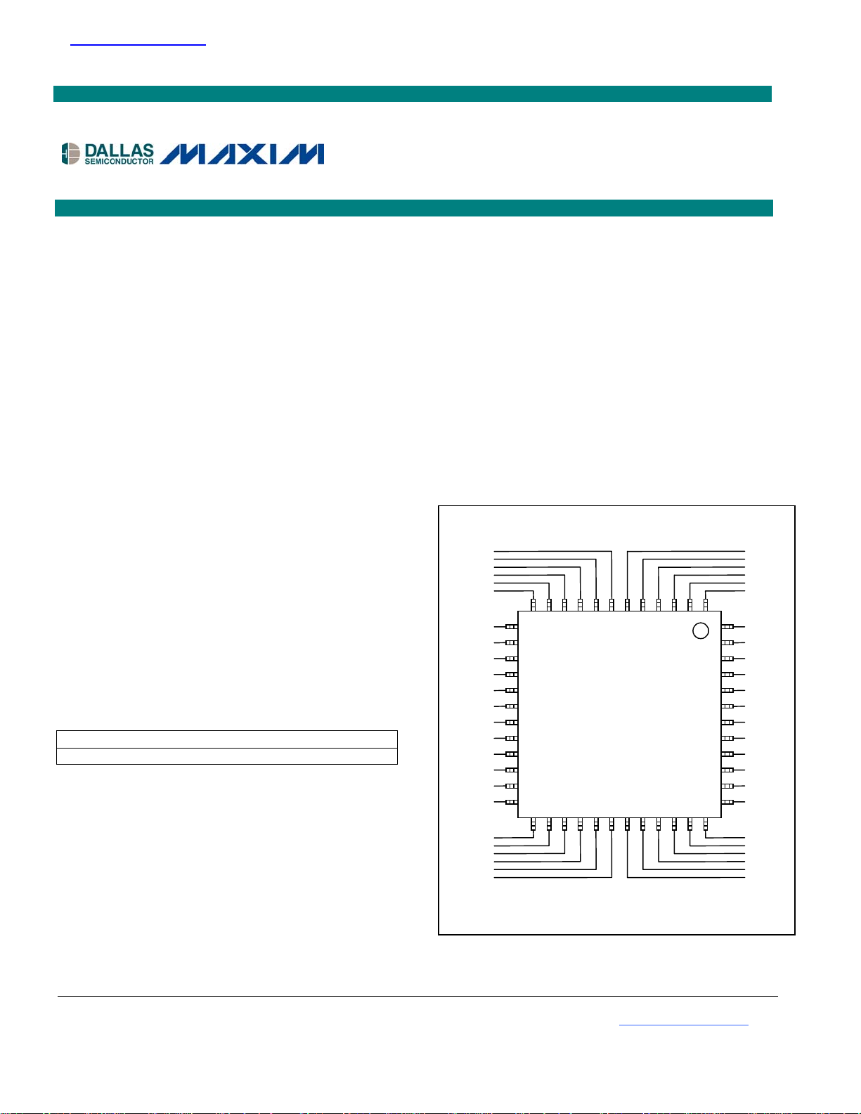
V
R1P
R1N
R2P
R2N
R3P
R3N
R4P
R4N
R5P
R5N
R6P
R6N
R7P
R7N
R8P
R8N
GND
REF
9
101112
13
14
15
16
17
18
19
20
21
22
23
24
25 26 27 28 29 30
Semiconductor
Dallas
DS2125
31 32 33 34 35 36
LQFP
3 4 5 6 7 8
12
48
47
46
45
44
43
42
41
40
39
38
37
Signals
PIN CONFIGURATION
TOP VIEW
HS_GND
HS_GND
HS_GND
HS_GND
HS_GND
HS_GND
HS_GND
HS_GND
HS_GND
TPWR
R15N
R15P
R14N
R14P
R13N
R13P
R12N
R12P
R11N
R11P
R10N
R10P
R9N
R9P
ISO
DIFFSENSE
DIFF_CAP
HS_GND
HS_GND
HS_GND
Note: Some revisions of this device may incorporate deviations from published specifications known as errata. Multiple revisions of any device
may be simultaneously available through various sales channels. For information about device errata, click here: www.maxim-ic.com/errata
.
1 of 7
REV: 052604
Page 2
DS2125 Ultra3 LVD/SE SCSI 15-Line Terminator
ABSOLUTE MAXIMUM RATINGS
V
, ISO, GND, DIFFSENSE, DIFF_CAP, TPWR, RxP, RxN (x = 1 . . . 15) -0.3V, +6.0V
REF
V
Continuous Output Current ±200mA
REF
Continuous Power Dissipation (T
= +70°C), 48-Pin LQFP
A
2W
Operating Temperature Range 0°C to +70°C
Junction Temperature +150°C
Storage Temperature Range -65°C to +160°C
Lead Temperature (soldering, 10s) +300°C
Stresses beyond those listed under “Absolute Maximum Ratings” may cause permanent damage to the device. These are stress ratings only,
and functional operation of the device at these or any other conditions beyond those indicated in the operational sections of the specifications is
not implied. Exposure to the absolute maximum rating conditions for extended periods may affect device reliability.
ELECTRICAL CHARACTERISTICS
(TPWR = 3.3V, TA = 0°C to +70°C, unless otherwise noted.)
PARAMETER SYMBOL CONDITIONS MIN TYP MAX UNITS
TPWR Operating Supply
Range
V
TPWR
LVD
SE
TPWR SUPPLY CURRENT
TPWR Supply Current
(All Lines Open)
I
TPWR_LVD
I
TPWR_SE
I
TPWR_ISO
LVD SCSI mode
SE SCSI mode
ISO mode (terminators disabled)
LVD TERMINATION (Applies to each line pair, 1 to 15 in LVD mode)
Differential-Mode
Termination Resistance
Common-Mode
Termination Resistance
R
100 110
DM
RP and RN shorted together 110 165
R
CM
Differential-Mode Bias VDM All lines open 100 125 mV
Common-Mode Bias VCM RP and RN shorted together 1.15 1.25 1.35 V
SE TERMINATION (Applies to SE terminators, 1 to 15 in SE mode)
= (VLx - 0.2) / ILx,
R
Single-Ended Mode
Termination Resistance
SE
where V
R
SE
pin with pin unloaded and
= current for each terminator pin
I
Lx
= voltage at terminator
Lx
with the pin forced to 0.2V (Note 2)
(Note 2)
SE Voltage Reference V
SE
REF
Signal level at 0.5V -18.0 -22.4
(Note 2) 2.7 2.85 3.0 V
Signal level at 0.2V, all lines low -21.0 -24 -25.4 Termination Current
I
Pin Leakage With ISO high 400 nA
Single-Ended GND
Resistance
Measured at RP pins, I = 10mA 20 60
R
GND
TERMINATOR PIN CAPACITANCE
Terminator Pin
Capacitance
V
REGULATOR
REF
1.25V Regulator Output
Voltage
1.25V Regulator ShortCircuit Source Current
1.25V Regulator ShortCircuit Sink Current
1.25V Regulator Line
Regulation
With ISO high (Note 1) 3 pF
C
IN
V
I
1.15 1.25 1.35 V
REF_LVD
V
SOURCE
V
I
SINK
= 0V -375 -700 -1000 mA
REF
= 3.3V 170 300 700 mA
REF
unloaded; vary TPWR from
V
REF
2.7V to 5.5V
2.85V Regulator (Note 2) 2.7 2.85 3.0 V
2.85V Regulator ShortCircuit Source Current
2.85V Regulator ShortCircuit Sink Current
V
= 0V (Note 2) -375 -700 -1000 mA
REF
V
= 3.3V (Note 2) 170 300 700 mA
REF
2 of 7
2.7 5.5
4.0 5.5
20 32
1.6 10
250 750
V
mA
mA
mA
W
W
104.5 110 115.5
W
mA
W
1.0 2.5
%
Page 3
DS2125 Ultra3 LVD/SE SCSI 15-Line Terminator
ELECTRICAL CHARACTERISTICS (continued)
(TPWR = 3.3V, TA = 0°C to +70°C, unless otherwise noted.)
PARAMETER SYMBOL CONDITIONS MIN TYP MAX UNITS
V
REGULATOR
REF
2.85V Regulator Line
Regulation
V
unloaded; vary TPWR from
REF
4.0V to 5.5V
1.0 2.5
%
DIFFSENS OUTPUT
DIFFSENS Driver Output
Voltage
DIFFSENS Driver Source
Current
DIFFSENS Driver Sink
Current
DIFFSENS Leakage
(Note 3)
V
DSO
I
V
DSH
V
I
DSL
I
LEAK, LOW
I
LEAK, HIGH
-5mA £ I
DIFFSENS
DIFFSENS
DFFSENS
= 0V -15 -5 mA
= 3.3V 100 200
With ISO high, |V
With ISO high, |V
0.3V
£ 50mA
DIFFSENS
DIFFSENS
| = 0.3V -3 +1
- V
TPWR
| =
1.2 1.4 V
mA
1 3
mA
THERMAL SHUTDOWN
Thermal-Shutdown
Threshold
Thermal-Shutdown
Hysteresis
(Note 1) 10
For increasing temperature
(Note 1)
150
°C
°C
MODE CHANGE DELAY/FILTER
Mode Change Delay t
0.66 1.25 2.00 ms
DELAY
LOGICAL SIGNALS (ISO)
Input Low Voltage VIL -0.3 +0.8 V
Input High Voltage VIH 2
Input Current IIL VCC = 3.3V -30 -10
TPWR
+ 0.3
V
mA
DIFF_CAP
Input Current IL V
DIFF_CAP SE
Operating Range
DIFF_CAP LVD
Operating Range
DIFF_CAP HVD
Operating Range
Note 1: Guaranteed by design.
Note 2: TPWR = 4.0V.
Note 3: Room temperature only.
-0.3 +0.5 V
V
SEOR
0.7 1.9 V
V
LVDOR
V
2.4
HVDOR
= -0.3V -1 +1
IL
V
TPWR
0.3
+
mA
V
PIN DESCRIPTION
PIN NAME FUNCTION
1, 2, 11–26,
37–48
3 TPWR
4–9, 28–33 HS_GND Heat-Sink Ground. Internally connected to the mounting pad. This should be grounded.
10 V
27 GND Ground. Signal ground, 0V.
34 DIFF_CAP
35 DIFFSENSE DIFFSENSE. Output to drive the SCSI bus DIFFSENS line.
RxP, RxN Signal Termination. Connect to SCSI bus signal lines.
Termination Power. Connect to the SCSI TERMPWR line and decouple with a 2.2mF
capacitor.
REF
decoupled with a 4.7mF capacitor.
Reference Voltage. 2.85V reference in SE mode and 1.25V reference in LVD mode; must be
DIFFSENSE Capacitor. Connect a 0.1mF capacitor for the DIFFSENSE filter. Input to detect
the type of device (differential or single-ended) on the SCSI bus.
36 ISO Isolation. When pulled high, the DS2125 isolates its bus pins (RxN, RxP) from the SCSI bus.
3 of 7
Page 4

Figure 1. Block Diagram
DS2125 Ultra3 LVD/SE SCSI 15-Line Terminator
DIFF_CAP
V
REF
DIFFSENSE
THERMAL-
SHUTDOWN
CIRCUITRY
DIFFENSE
CIRCUITRY
SE
LVD
HVD
ISO
CONTROL
LOGIC
V
REF
10W
10W
BANDGAP
1.25V
+
-
+
-
Dallas
Semiconductor
DS2125
+
-
R1N
R15N
R1P
R15P
SE GND
DRIVER
4 of 7
Page 5

DS2125 Ultra3 LVD/SE SCSI 15-Line Terminator
m
Figure 2. SCSI Bus Configuration
TERMPWR
TERMPWR
TPWR
ISO
CONTROL LINES (15)
TPWR
ISO
V
DIFFSENS
DIFF_CAP
REF
4.7
F
20kW 20kW
0.1mF
DIFFSENSE
DIFFSENS
DIFF_CAP
0.1mF
V
REF
4.7mF
TPWR
ISO
CONTROL LINES (15)
TPWR
ISO
V
REF
DIFFSENS
DIFF_CAP
DIFFSENS
DIFF_CAP
V
REF
4.7mF
4.7mF
Note: The following terms are used throughout this data sheet:
DIFFSENS: Refers to the SCSI bus signal.
DIFFSENSE: Refers to the DS2125 pin name and internal circuitry capable of driving the DIFFSENS line.
DIFF_CAP: Refers to the DS2125 pin name and internal circuitry relating to monitoring the DIFFSENS line.
DETAILED DESCRIPTION
The DS2125 combines LVD and SE termination with DIFFSENSE sourcing and detection. A bandgap reference is
fed into two amplifiers, which creates a 1.25V reference voltage and a 2.85V reference voltage. The control logic
determines which of these references are applied to the termination resistors. If the SCSI bus is in LVD mode, the
1.25V reference is used. If the SCSI bus is in SE mode, the 2.85V reference is used. That same control logic
switches in/out parallel resistors to change the total termination resistance accordingly. Finally, in SE mode the R
pins are switched to ground.
p
The DIFFSENSE circuitry decodes trinary logic. There is one of three voltages on the SCSI control line called
DIFFSENS. Two comparators and a NAND gate determine if the voltage is below 0.6V, above 2.15V, or in
between, which indicates the mode of the bus as SE, HVD, or LVD, respectively.
5 of 7
Page 6

DS2125 Ultra3 LVD/SE SCSI 15-Line Terminator
The DS2125’s DIFF_CAP pin monitors the DIFFSENS line to determine the device’s proper operating mode. The
DIFFSENSE pin can also drive the SCSI DIFFSENS line to determine the SCSI bus-operating mode. The DS2125
switches to the termination mode that is appropriate for the bus based on the value of the DIFFSENS voltage.
These modes are LVD mode, SE mode, and HVD isolation mode.
LVD MODE
A precision laser-trimmed resistor string with two amplifiers provides LVD termination. This configuration yields
105W differential and 150W common-mode impedance. A 112mV fail-safe bias is maintained when no drivers are
connected to the SCSI bus.
SE MODE
When the external driver for a given signal line turns off, the active terminator pulls that signal line to 2.85V
(quiescent state). The terminating resistors maintain their 110W value.
HVD ISOLATION MODE
The DS2125 identifies that there is an HVD device on the SCSI bus and isolates the termination pins from the bus.
When ISO is pulled high, the termination pins are isolated from the SCSI bus, and V
thermal shutdown, the termination pins are isolated from the SCSI bus, and V
becomes high impedance. The
REF
remains active. During
REF
DIFFSENSE driver is shut down during either of these two events. An internal pulldown resistor assures that the
DS2125 is terminating the bus if the ISO pin is left floating.
To ensure proper operation, the TPWR pin should be connected to the SCSI bus TERMPWR line. As with all
analog circuitry, the TERMPWR and V
lines should be bypassed locally. A 2.2mF capacitor and a 0.01mF high-
DD
frequency capacitor are recommended between TPWR and ground, and placed as close as possible to the
DS2125. The DS2125 should be placed as close as possible to the SCSI connector to minimize signal and power
trace length, thereby resulting in less input capacitance and reflections, which can degrade the bus signals.
To maintain the specified regulation, a 4.7mF capacitor is required between the V
DS2125. A high-frequency capacitor (0.1mF ceramic recommended) can also be placed on the V
pin and ground of each
REF
pin in
REF
applications that use fast rise/fall-time drivers. Figure 2 shows a typical SCSI bus configuration.
REFERENCE DOCUMENTS
TITLE
SCSI Parallel Interface 2 (SPI-2) Project: 1142-M, 1998 ftp://ftp.t10.org/t10/drafts/spi2/spi2r20b.pdf X3.302:1998
SCSI Parallel Interface 3 (SPI-3) Project: 1302-D, 1999 ftp://ftp.t10.org/t10/drafts/spi3/spi3r14.pdf NCITS.336:2000
SCSI Parallel Interface 4 (SPI-4) Project: 1365-D, 200x ftp://ftp.t10.org/t10/drafts/spi4/spi4r10.pdf INCITS.362:2002
T10 PROJECT
DOCUMENT
T10 COMMITTEE FTP LINK
ANSI
DOCUMENT NO.
SUPPLIERS
SUPPLIER PHONE WEBSITE
American National Standards Institute (ANSI) 212-642-4900 www.ansi.org/
Global Engineering Documents 800-854-7179 http://global.ihs.com/
CHIP INFORMATION
TRANSISTOR COUNT: 8382 MOS and 87 BiPOLAR
PROCESS: BiCMOS
SUBSTRATE CONNECTED TO GROUND
THERMAL INFORMATION
Theta-JA: 65°C/W
6 of 7
Page 7

DS2125 Ultra3 LVD/SE SCSI 15-Line Terminator
PACKAGE INFORMATION
(The package drawing(s) in this data sheet may not reflect the most current specifications. For the latest package outline
information, go to www.maxim-ic.com/DallasPackInfo.)
7 of 7
Maxim/Dallas Semiconductor cannot assume responsibility for use of any circuitry other than circuitry entirely embodied in a Maxim/Dallas Semiconductor product.
No circuit patent licenses are implied. Maxim/Dallas Semiconductor reserves the right to change the circuitry and specifications without notice at any time.
Maxim Integrated Products, 120 San Gabriel Drive, Sunnyvale, CA 94086 408-737-7600
are registered trademarks of Maxim Integrated Products, Inc., and Dallas Semiconductor Corporation.
© 2004 Maxim Integrated Products · Printed USA
 Loading...