

r
查询DS2119M供应商
Ultra3 LVD/SE SCSI Terminato
DS2119M
www.maxim-ic.com
FEATURES
Fully compliant with SCSI SPI-2, SPI-3,
SPI-4, Ultra160, and Ultra320
Provides multimode low-voltage
differential/single-ended (LVD/SE)
termination for nine signal-line pairs
Auto-selection of LVD or SE termination
5% tolerance on SE and LVD termination
resistance
Low power-down capacitance of 3pF
Onboard thermal-shutdown circuitry
SCSI-bus hot-plug compatible
Fully supports actively negated SE SCSI
signals
PIN ASSIGNMENT
VREF
RIP
RIN
R2P
R2N
HS GND
R3P
R3N
R4P
R4N
R5P
R5N
ISO
GND
1
2
3
4
5
6
7
8
9
10
11
12
13
14
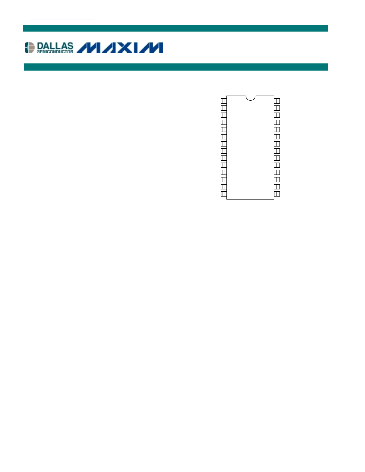
DS2119ME 28-Pin TSSOP
28
27
26
25
24
23
22
21
20
19
18
17
16
15
TPWR
TPWR
R9N
R9P
R8N
R8P
HS GND
R7N
R7P
R6N
R6P
DIFF_CAP
DIFFSENSE
MSTR/SLV
DESCRIPTION
The DS2119M Ultra3 LVD/SE SCSI Terminator is both a low-voltage differential (LVD) and singleended (SE) terminator. The multimode operation enables the designer to implement LVD in current
products while allowing the end-user SE-backward compatibility with legacy devices. If the device is
connected in an LVD-only bus, the DS2119M will use LVD termination. If any SE devices are connected
to the bus, the DS2119M will use SE termination. This is accomplished automatically inside the part by
sensing the voltage on the SCSI bus DIFFSENS line.
For the LVD termination, the DS2119M integrates two current sources with nine precision resistor
strings. For the SE termination, one regulator and nine precision 110Ω resistors are used. Three
DS2119M terminators are needed for a wide SCSI bus.
REFERENCE DOCUMENTS
Small Computer Systems Interface (SCSI-3) SCSI Parallel Interface (SPI) Project: 0855-M, 1995
Small Computer Systems Interface (SCSI-3) SCSI Parallel Interface 2 (SPI-2) Project: 1142-M, 1998
Small Computer Systems Interface (SCSI-3) SCSI Parallel Interface 3 (SPI-3) Project: 1302-D, 1999
Small Computer Systems Interface (SCSI-3) SCSI Parallel Interface 4 (SPI-4) Project: 1365-D, 200x
Available From:
American National Standards Institute (ANSI) Phone: (212) 642-4900
Global Engineering Documents 15 Inverness Way East; Englewood, CO 80112 Phone: (800) 854-7179
1 of 9 022002

DS2119M
FUNCTIONAL DESCRIPTION
The DS2119 combines LVD and SE termination with DIFFSENS sourcing and detection.
A bandgap reference is fed into two amplifiers, which creates a 1.25V reference voltage and a 2.85V
reference voltage. The control logic determines which of these references will be applied to the
termination resistors. If the SCSI bus is in LVD mode, then the 1.25V reference will be used. If the SCSI
bus is in SE mode, then the 2.85V reference will be used. That same control logic will switch in/out
parallel resistors to change the total termination resistance accordingly. Finally, in SE mode, the Rp pins
will be switched to ground.
The DIFFSENSE circuitry decodes trinary logic. There will be one of three voltages on the SCSI control
line called DIFFSENS. Two comparators and a NAND gate determine if the voltage is below 0.6V, above
2.15V, or in between. That indicates the mode of the bus to be SE, HVD, or LVD, respectively.
The DS2119M’s DIFF_CAP pin monitors the DIFFSENS line to determine the proper operating mode of
the device. The DIFFSENSE pin can also drive the SCSI DIFFSENS line (when MSTR/SLV = 1) to
determine the SCSI bus-operating mode. The DS2119M switches to the termination mode that is
appropriate for the bus based on the value of the DIFFSENS voltage. These modes are:
LVD Mode: LVD termination is provided by a precision laser-trimmed resistor string with two
current sources. This configuration yields a 105Ω differential and 150Ω common-mode
impedance. A fail-safe bias of 112mV is maintained when no drivers are connected to the SCSI
bus.
SE Mode: When the external driver for a given signal line turns off, the active terminator will pull
that signal line to 2.85V (quiescent state). When used with an active negation driver, the power
amp can sink 22mA per line and the reference voltage will move less than 100mV. The
terminating resistors maintain their 110Ω=value.
HVD Isolation Mode: The DS2119M identifies that there is an HVD (high-voltage differential)
device on the SCSI bus and isolates the termination pins from the bus.
When ISO = 1, the termination pins are isolated from the SCSI bus, V
shutdown, the termination pins are isolated from the SCSI bus and V
DIFFSENSE driver is shut down during either of these two events.
To ensure proper operation, the TPWR pin should be connected to the SCSI bus TERMPWR line. As
with all analog circuitry, the TERMPWR and V
lines should be bypassed locally. A 2.2µF capacitor
DD
and a 0.01µF high-frequency capacitor are recommended between TPWR and ground and placed as close
as possible to the DS2119M. The DS2119M should be placed as close as possible to the SCSI connector
to minimize signal and power-trace length, thereby resulting in less input capacitance and reflections,
which can degrade the bus signals.
remains active. During thermal
REF
becomes high impedance. The
REF
2 of 9

DS2119M
To maintain the specified regulation, a 4.7µF capacitor is required between the V
pin (VREF) and
REF
ground of each DS2119M. A high frequency cap (0.1µF ceramic recommended) can also be placed on the
V
pin in applications that use fast rise/fall time drivers. A typical SCSI bus configuration is shown in
REF
Figure 2.
DIFFSENS Noise Filtering: The DS2119M incorporates a digital filter to remove high-frequency
transients on the DIFFSENS control line, thereby eliminating erroneous switching between
modes. This filter eliminates the need for the external capacitor and resistor, which heretofore
performed this function.
NOTES:
1) DIFFSENS. Refers to the SCSI bus signal.
2) DIFFSENSE. Refers to the Dallas Semiconductor pin name and internal circuitry relating the
DIFFSENS driver.
3 of 9

Figure 1. DS2119M BLOCK DIAGRAM
DS2119M
4 of 9

Figure 2. SCSI BUS CONFIGURATION
DS2119M
5 of 9

DS2119M
Table 1. PIN DESCRIPTION
PIN SYMBOL DESCRIPTION
1 VREF Reference Voltage. 2.85V reference in SE mode and 1.25V reference in
LVD mode; must be decoupled with a 4.7µF cap.
2–5, 7–12,
18–21, 23–26
RxP,
RxN
Signal Termination. Connect to SCSI bus signal lines.
6, 22 HS GND Heat Sink Ground. Internally connected to the mounting pad. Should
be grounded.
13 ISO Isolation. When pulled high, the DS2119M isolates its bus pins (RxP,
RxN) from the SCSI bus.
14 GND Ground. Signal ground; 0V.
15 MSTR/SLV Master/Slave. Mode-select for the noncontrolling terminator. When
pulled high, MSTR enables the DIFFSENSE driver.
16 DIFFSENSE DIFFSENSE. Output to drive the SCSI bus DIFFSENS line.
17 DIFF_CAP DIFFSENSE CAPACITOR. Connect a 0.1µF capacitor for
DIFFSENSE filter. Input to detect the type of device (differential or
single-ended) on the SCSI bus.
27, 28 TPWR Termination Power. Connect to the SCSI TERMPWR line and
decouple with a 2.2µF capacitor.
RECOMMENDED OPERATING CONDITIONS
PARAMETER SYMBOL MIN TYP MAX UNITS NOTES
Termpower Voltage
SE Mode
LVD Mode
V
Logic 0 VIL -0.3 +0.8 V
Logic 1 VIH 2.0 V
Operating Temperature V
V
TPWR
TPWR
(SE)
(LVD)
0 70 °C
AMB
4.0
2.7
5.5
5.5
+ 0.3 V
TPWR
V
V
6 of 9

DS2119M
SINGLE-ENDED CHARACTERISTICS
PARAMETER SYMBOL MIN TYP MAX UNITS NOTES
SE Termination
RSE 104.5 110 115.5 Ω 1
Resistance
SE Voltage Reference V
SE Output Current l
Output Capacitance C
2.7 2.85 3.0 V
REF
25.4 mA 2
OSE
3 pF 3
OUT
LOW-VOLTAGE DIFFERENTIAL CHARACTERISTICS
PARAMETER SYMBOL MIN TYP MAX UNITS NOTES
Differential Mode
Termination Resistance
Common Mode
Termination Resistance
RDM 100
RCM 110
110 Ω
190
Ω
Differential Mode Bias VDM 100 125 mV 4
Common Mode Bias VCM 1.125 1.375 V
DC CHARACTERISTICS
PARAMETER SYMBOL MIN TYP MAX UNITS NOTES
Termpower Current I
Input Leakage High IIH -1.0 µA
Input Leakage Low IIL 1.0 µA
Output Current High IOH -1.0 mA 5, 7
Output Current Low IOL 4.0 mA 6, 7
DIFFSENS SE
Operating Range
DIFFSENS LVD
Operating Range
DIFFSENS HVD
Operating Range
V
V
DIFFSENSE Driver
Output Voltage
DIFFSENSE Driver
Source Current
DIFFSENSE Driver
Sink Current
Thermal Shutdown 150 ºC 3
12 mA 4
TPMR
V
-0.3 0.5 V
SEOR
0.7 1.9 V
LVDOR
2.4 V
HVDOR
V
1.2 1.4 V 8, 9
DSO
5 15 mA 8, 10, 12
I
DSH
20 200 µA 8, 11
I
DSL
+ 0.3 V
TPWR
7 of 9

DS2119M
REGULATOR CHARACTERISTICS (0°C to +70°C)
PARAMETER SYMBOL MIN TYP MAX UNITS NOTES
Line Regulation LI
Load Regulation LO
Current Limit I
Sink Current I
NOTES:
1) V
2) V
3) Guaranteed by design.
4) All lines open.
5) V
6) V
7) SE/LVD/HVD pins only.
8) MSTR/SLV = 1.
9) I
10) V
11) V
12) TPWR = 5.5V.
= 0V to 3V.
LINE
= 0.2V.
LINE
= 2.4V.
OUT
= 0.4V.
OUT
= 0mA to 5mA.
DS
= 0V.
DSO
= 2.75V.
DSO
1.0 2.5 %
REG
1.3 3.5 %
REG
550 mA
LIM
200 mA
SINK
8 of 9

DS2119M 28-PIN SSOP PACKAGE
R
R
DS2119M
NOTES:
1) DIMENSION “D” DOES NOT INCLUDE MOLD MISMA TCH, FLASH, O
PROTRUSIONS. MOLD MISMATCH, FLASH, AND PROTRUSIONS
SHALL NOT EXC EED 0.15 PER SIDE.
2) DIMENSION “B” DOES NOT INCLUDE DAMBAR PROTRUSION.
DAMBAR PROTRUSION SHALL NOT BE LOCATED ON THE LOWE
RADIUS OF THE FOOT.
PKG 28-PIN
DIM MIN MAX
A
MM
A1
MM
A2
MM
c
MM
L
MM
e1
MM
b
MM
D
MM
E1
MM
E
MM
- 1.10
0.05 -
0.75 1.05
0.09 0.20
0.50 0.75
0.65 BSC
0.18 0.30
9.60 9.80
4.40 BSC
6.20 6.60
9 of 9
 Loading...