

General Description
The DS2045W is a 1Mb reflowable nonvolatile (NV)
SRAM, which consists of a static RAM (SRAM), an NV
controller, and an internal rechargeable manganese
lithium (ML) battery. These components are encased in
a surface-mount module with a 256-ball BGA footprint.
Whenever VCCis applied to the module, it recharges the
ML battery, powers the SRAM from the external power
source, and allows the contents of the SRAM to be modified. When V
CC
is powered down or out of tolerance,
the controller write-protects the SRAM’s contents and
powers the SRAM from the battery. The DS2045W also
contains a power-supply monitor output, RST, which can
be used as a CPU supervisor for a microprocessor.
Applications
RAID Systems and Servers POS Terminals
Industrial Controllers Data-Acquisition Systems
Gaming Fire Alarms
Router/Switches PLC
Features
♦ Single-Piece, Reflowable, 27mm2PBGA Package
Footprint
♦ Internal ML Battery and Charger
♦ Unconditionally Write-Protects SRAM when V
CC
is Out-of-Tolerance
♦ Automatically Switches to Battery Supply when
V
CC
Power Failures Occur
♦ Internal Power-Supply Monitor Detects Power Fail
Below Nominal V
CC
(3.3V)
♦ Reset Output can be used as a CPU Supervisor
for a Microprocessor
♦ Industrial Temperature Range (-40°C to +85°C)
♦ UL Recognized
DS2045W
DS2045W 3.3V Single-Piece 1Mb
Nonvolatile SRAM
______________________________________________ Maxim Integrated Products 1
Rev 1; 1/05
For pricing, delivery, and ordering information, please contact Maxim/Dallas Direct! at
1-888-629-4642, or visit Maxim’s website at www.maxim-ic.com.
Ordering Information
Pin Configuration appears at end of data sheet.
PART TEMP RANGE PIN-PACKAGE
SUPPLY TOLERANCE (%)
DS2045W-100 -40°C to +85°C 256 Ball 27mm
2
BGA Module
100 3.3V ±0.3V
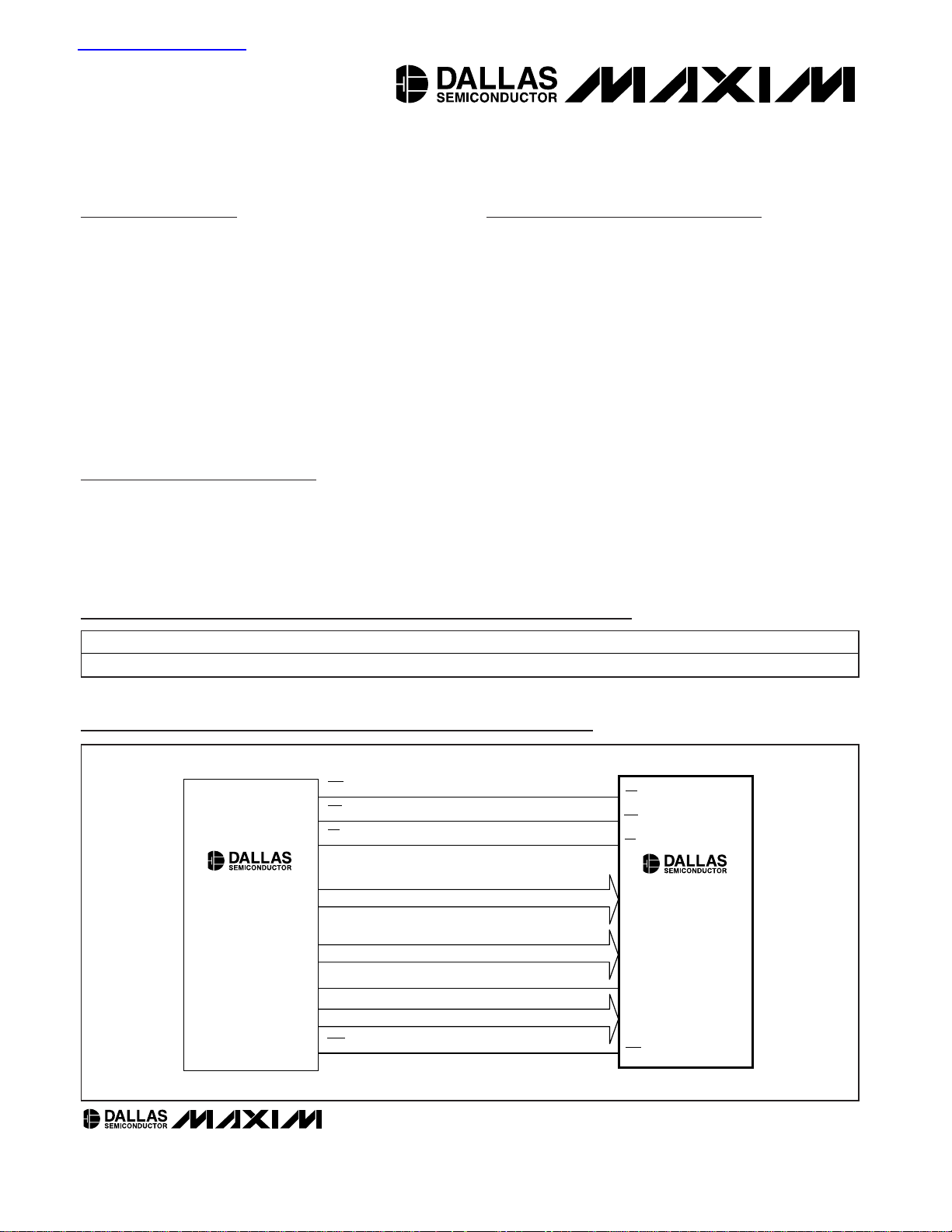
Typical Operating Circuit
P4.0
P3.6
P3.7
P1.0–7
AD0–AD7
P4.4
P2.0–7
P3.2
RST
A8–15
A0–7
A16
DQ0–7
OE
WE
CE
8 BITS
8 BITS
8 BITS
(CE0)
(INT0)
8051
MICROPROCESSOR
DS2045W
128k x 8
NV SRAM
(WR)
(RD)
查询DS2045W供应商
SPEED (ns)
DS2045W
DS2045W 3.3V Single-Piece 1Mb
Nonvolatile SRAM
2 _____________________________________________________________________
ABSOLUTE MAXIMUM RATINGS
RECOMMENDED OPERATING CONDITIONS
(TA= -40°C to +85°C)
Stresses beyond those listed under “Absolute Maximum Ratings” may cause permanent damage to the device. These are stress ratings only, and functional
operation of the device at these or any other conditions beyond those indicated in the operational sections of the specifications is not implied. Exposure to
absolute maximum rating conditions for extended periods may affect device reliability.
Voltage on Any Pin Relative to Ground .................-0.3V to +4.6V
Operating Temperature Range ...........................-40°C to +85°C
Storage Temperature Range ...............................-40°C to +85°C
Soldering Temperature...................See IPC/JEDEC J-STD-020C
PARAMETER
CONDITIONS
Supply Voltage V
CC
3.0 3.3 3.6 V
Input Logic 1 V
IH
2.2
V
Input Logic 0 V
IL
0 0.4 V
CAPACITANCE
(TA= +25°C)
PARAMETER
SYMBOL
CONDITIONS
MIN
TYP
MAX
UNITS
Input Capacitance C
IN
Not tested 7 pF
Input/Output Capacitance C
OUT
Not tested 7 pF
DC ELECTRICAL CHARACTERISTICS
(VCC= 3.3V ±0.3V, TA= -40°C to +85°C.)
PARAMETER
CONDITIONS
UNITS
Input Leakage Current I
IL
µA
I/O Leakage Current I
IO
CE = V
CC
µA
Output-Current High I
OH
At 2.4V
mA
Output-Current Low I
OL
At 0.4V 2.0 mA
Output-Current Low RST
At 0.4V (Note 1)
mA
I
CCS1
CE = 2.2V 0.5 7
Standby Current
I
CCS2
CE = V
CC
- 0.2V 0.2 5
mA
Operating Current I
CCO1tRC
= 200ns, outputs open 50 mA
Write Protection Voltage V
TP
2.8 2.9 3.0 V
SYMBOL
SYMBOL
MIN TYP MAX UNITS
V
CC
MIN TYP MAX
-1.0 +1.0
-1.0 +1.0
-1.0
IOL RST
10.0
DS2045W
DS2045W 3.3V Single-Piece 1Mb
Nonvolatile SRAM
_____________________________________________________________________ 3
POWER-DOWN/POWER-UP TIMING
(TA= -40°C to +85°C)
PARAMETER
SYMBOL
CONDITIONS
UNITS
VCC Fail Detect to CE and WE Inactive t
PD
(Note 7) 1.5 µs
VCC Slew from VTP to 0V t
F
µs
VCC Slew from 0V to V
TP
t
R
µs
VCC Valid to CE and WE Inactive t
PU
2ms
VCC Valid to End of Write Protection t
REC
125 ms
VCC Fail Detect to RST Active t
RPD
(Note 1) 3.0 µs
VCC Valid to RST Inactive t
RPU
(Note 1)
525 ms
DATA RETENTION
(TA= +25°C)
PARAMETER
SYMBOL
CONDITIONS
MIN
TYP
MAX
UNITS
Expected Data-Retention Time (Per Charge) t
DR
(Note 8) 2 3
years
AC ELECTRICAL CHARACTERISTICS
(VCC= 3.3V ±0.3V, TA= -40°C to +85°C.)
DS2045W-100
PARAMETER
CONDITIONS
MIN MAX
UNITS
Read Cycle Time
t
RC
100 ns
Access Time
t
ACC
100 ns
OE to Output Valid
t
OE
50 ns
CE to Output Valid
t
CO
100 ns
OE or CE to Output Active
t
COE
(Note 2) 5 ns
Output High Impedance from
Deselection
t
OD
(Note 2) 35 ns
Output Hold from Address Change
t
OH
5ns
Write Cycle Time
t
WC
100 ns
Write Pulse Width
t
WP
(Note 3) 75 ns
Address Setup Time
t
AW
0ns
t
WR1
(Note 4) 5
Write Recovery Time
t
WR2
(Note 5) 20
ns
Output High Impedance from WE
t
ODW
(Note 2) 35 ns
Output Active from WE
t
OEW
(Note 2) 5 ns
Data Setup Time
t
DS
(Note 6) 40 ns
t
DH1
(Note 4) 0
Data Hold Time
t
DH2
(Note 5) 20
ns
SYMBOL
MIN TYP MAX
150
150
225 350
DS2045W
DS2045W 3.3V Single-Piece 1Mb
Nonvolatile SRAM
4 _____________________________________________________________________
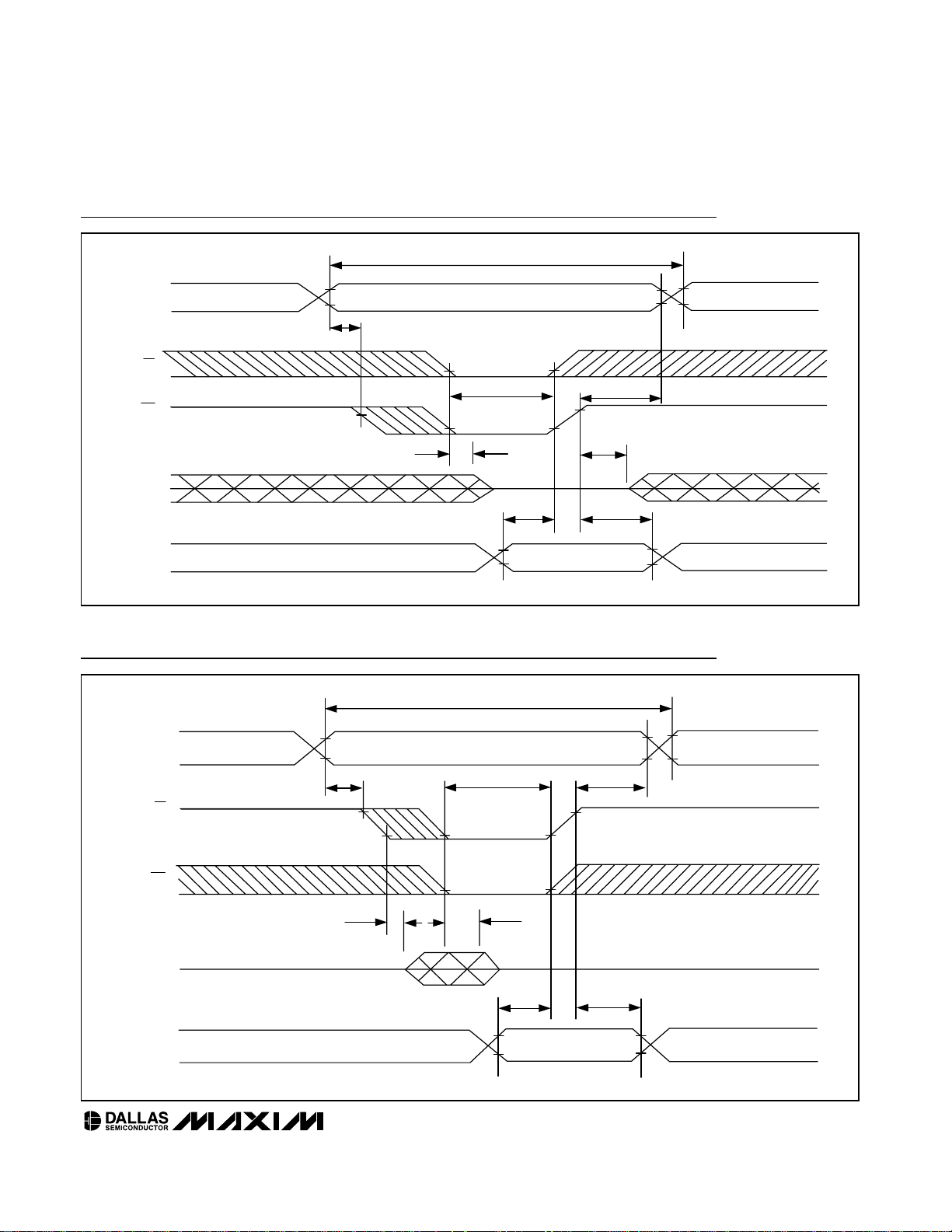
Read Cycle
OUTPUT
DATA VALID
t
RC
t
ACC
t
CO
t
OE
t
OH
t
OD
t
OD
t
COE
t
COE
V
IH
V
IH
V
IL
V
OH
V
OL
V
OH
V
OL
V
IL
V
IH
ADDRESSES
CE
OE
D
OUT
(SEE NOTE 9.)
V
IH
V
IH
V
IH
V
IH
V
IL
V
IL
V
IL
DS2045W
DS2045W 3.3V Single-Piece 1Mb
Nonvolatile SRAM
_____________________________________________________________________ 5
Write Cycle 1
DATA IN STABLE
ADDRESSES
CE
WE
D
OUT
D
IN
t
WC
V
IH
V
IH
V
IH
V
IH
V
IL
V
IL
V
IL
HIGH
IMPEDANCE
V
IH
V
IH
V
IL
V
IL
V
IH
V
IL
V
IL
V
IL
V
IL
t
AW
t
WP
t
OEW
t
DH1
t
DS
t
ODW
t
WR1
(SEE NOTES 2, 3, 4, 6, 10–13.)
Write Cycle 2
t
WC
t
AW
t
DH2
t
DS
t
COE
t
ODW
t
WP
t
WR2
V
IH
V
IL
V
IH
ADDRESSES
CE
WE
D
OUT
D
IN
V
IL
V
IH
V
IL
V
IH
V
IL
V
IL
V
IL
V
IL
V
IH
V
IH
V
IL
V
IH
DATA IN STABLE
V
IL
V
IH
V
IL
(SEE NOTES 2, 3, 5, 6, 10–13.)

DS2045W
DS2045W 3.3V Single-Piece 1Mb
Nonvolatile SRAM
6 _____________________________________________________________________
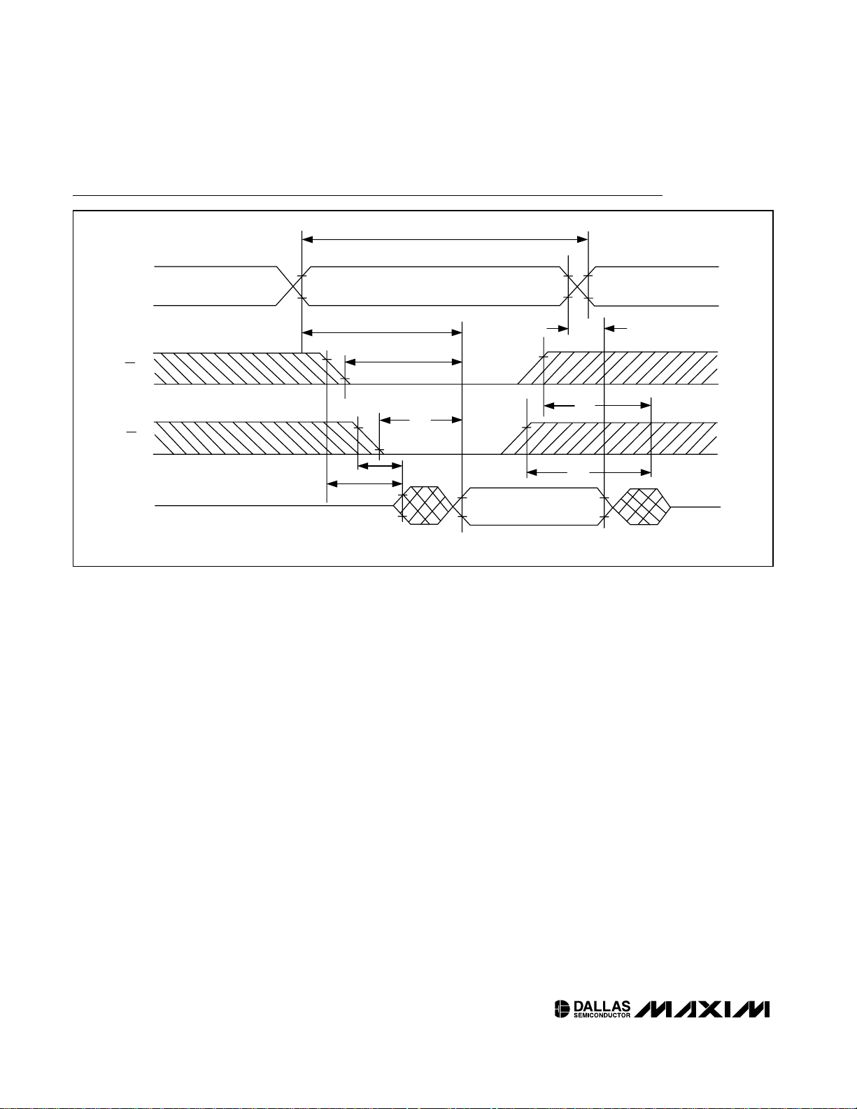
Power-Down/Power-Up Condition
t
DR
t
PU
t
F
t
PD
t
RPU
t
RPD
SLEWS WITH
V
CC
t
R
V
OL
V
IH
V
OL
t
REC
V
CC
V
TP
~2.5V
CE,
WE
RST
BACKUP CURRENT
SUPPLIED FROM
LITHIUM BATTERY
(SEE NOTES 1, 7.)
Note 1: RST is an open-drain output and cannot source current. An external pullup resistor should be connected to this pin to real-
ize a logic-high level.
Note 2: These parameters are sampled with a 5pF load and are not 100% tested.
Note 3: t
WP
is specified as the logical AND of CE and WE. tWPis measured from the latter of CE or WE going low to the earlier of
CE or WE going high.
Note 4: t
WR1
and t
DH1
are measured from WE going high.
Note 5: t
WR2
and t
DH2
are measured from CE going high.
Note 6: t
DS
is measured from the earlier of CE or WE going high.
Note 7: In a power-down condition, the voltage on any pin can not exceed the voltage on V
CC
.
Note 8: The expected t
DR
is defined as accumulative time in the absence of VCCstarting from the time power is first applied by the
user. Minimum expected data-retention time is based on a maximum of two +230°C convection solder reflow exposures,
followed by a fully charged cell. Full charge occurs with the initial application of V
CC
for a minimum of 96 hours. This para-
meter is assured by component selection, process control, and design. It is not measured directly in production testing.
Note 9: WE is high for a read cycle.
Note 10: OE = VIHor VIL. If OE = VIHduring write cycle, the output buffers remain in a high-impedance state.
Note 11: If the CE low transition occurs simultaneously with or latter than the WE low transition, the output buffers remain in a high-
impedance state during this period.
Note 12: If the CE high transition occurs prior to or simultaneously with the WE high transition, the output buffers remain in a high-
impedance state during this period.
Note 13: If WE is low or the WE low transition occurs prior to or simultaneously with the CE low transition, the output buffers remain
in a high-impedance state during this period.
Note 14: DS2045W BGA modules are recognized by Underwriters Laboratory (UL) under file E99151.
DS2045W
DS2045W 3.3V Single-Piece 1Mb
Nonvolatile SRAM
_____________________________________________________________________ 7
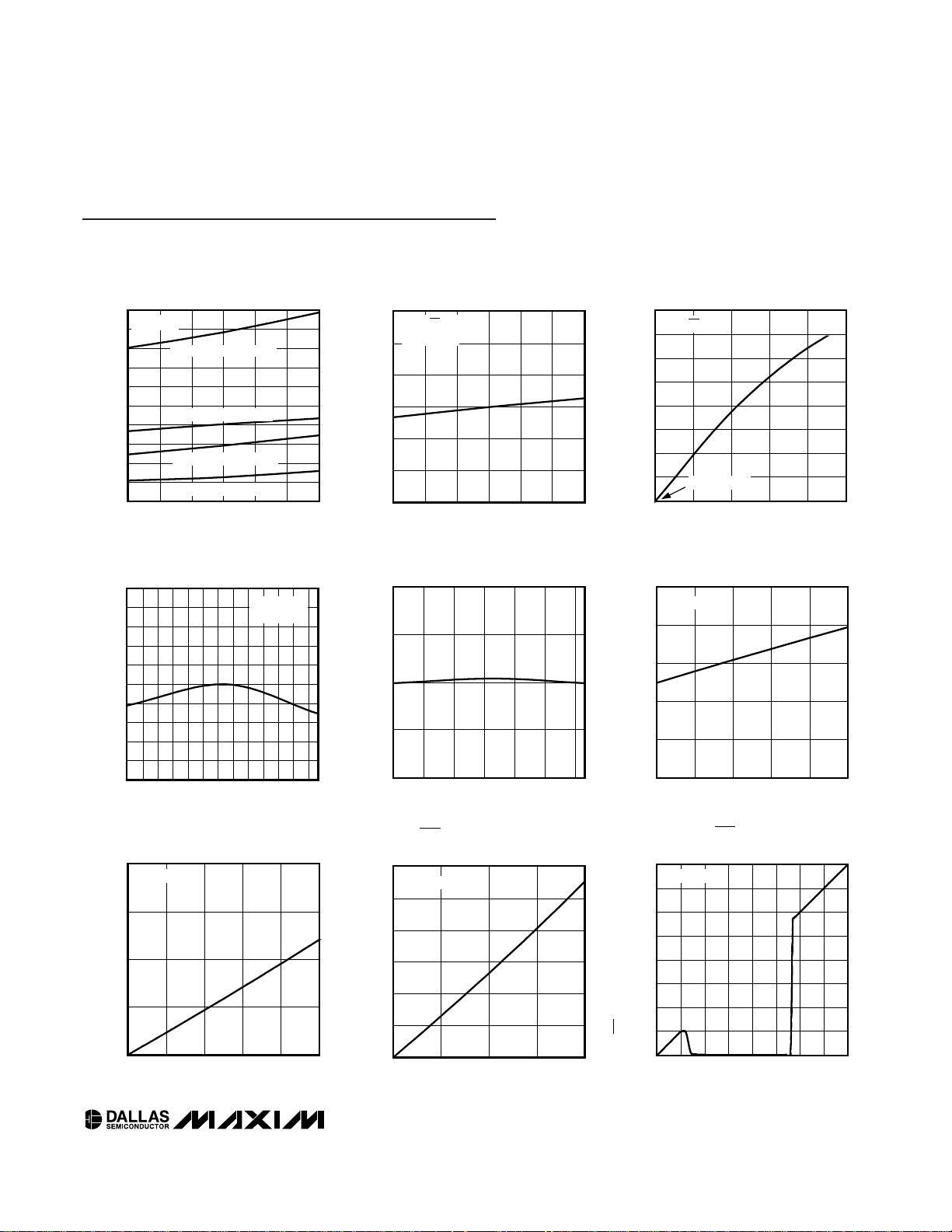
SUPPLY CURRENT
vs. OPERATING FREQUENCY
DS2045W toc01
VCC (V)
SUPPLY CURRENT (mA)
3.53.3
3.4
3.2
3.1
4
2
8
12
10
6
16
18
14
20
0
3.0 3.6
5MHz 100% DUTY CYCLE
5MHz 50% DUTY CYCLE
1MHz 100% DUTY CYCLE
1MHz 50% DUTY CYCLE
TA = +25°C
SUPPLY CURRENT
vs. SUPPLY VOLTAGE
DS2045W toc02
VCC (V)
SUPPLY CURRENT (µA)
3.5
3.3 3.4
3.1
3.2
130
140
150
160
170
180
120
3.0 3.6
VCC = CE
V
BAT
= V
CHRG
BATTERY CHARGER CURRENT
vs. BATTERY VOLTAGE
DS2045W toc03
DELTA BELOW V
CHRG
(V)
BATTERY CHARGER CURRENT, I
CHRG
(mA)
0.6 0.80.40.2
1
2
3
4
5
6
7
8
0
01.0
VCC = CE = 3.3V
V
CHRG
= 2.86V
V
CHRG
PERCENT CHANGE
vs. TEMPERATURE
DS2045W toc04
TEMPERATURE (°C)
V
CHRG
PERCENT CHANGE FROM +25°C (%)
80705060-10 0 10 20 30 40-30-20
-0.4
-0.3
-0.2
-0.1
0
0.1
0.2
0.3
0.4
0.5
-0.5
-40
VCC = 3.3V
V
BAT
= V
CHRG
VTP vs. TEMPERATURE
DS2045W toc05
TEMPERATURE (°C)
WRITE PROTECT, V
TP
(V)
80
60
20
40
0-20
2.85
2.90
2.95
3.00
2.80
-40
DQ VOH vs. DQ I
OH
DS2045W toc06
IOH (mA)
V
OH
(V)
-1-2-3-4
2.7
2.9
3.1
3.3
3.5
2.6
-5 0
VCC = 3.3V
DQ VOL vs. DQ I
OL
DS2045W toc07
IOL (mA)
V
OL
(V)
4132
0.1
0.2
0.3
0.4
0
05
VCC = 3.3V
RST OUTPUT-VOLTAGE LOW
vs. OUTPUT-CURRENT LOW
DS2045W toc08
IOL (mA)
V
OL
(V)
15105
0.1
0.2
0.3
0.5
0.4
0.6
0
020
VCC = 2.8V
RST VOLTAGE
vs. V
CC
DURING POWER-UP
DS2045W toc09
VCC POWER-UP (V)
RST VOLTAGE W/PULLUP RESISTOR (V)
3.52.5 3.01.0 1.5
2.0
0.5
0.5
1.0
1.5
2.0
2.5
3.0
3.5
4.0
0
0 4.0
TA = +25°C
Typical Operating Characteristics
(VCC= +3.3V, TA= +25°C, unless otherwise noted.)

DS2045W
DS2045W 3.3V Single-Piece 1Mb
Nonvolatile SRAM
8 _____________________________________________________________________
BALLS
NAME
DESCRIPTION
A1, A2, A3, A4
Ground
B1, B2, B3, B4 N.C. No Connection
C1, C2, C3, C4 A15 Address Input 15
D1, D2, D3, D4 A16 Address Input 16
E1, E2, E3, E4 RST
Open-Drain Reset Output
F1, F2, F3, F4 V
CC
Supply Voltage
G1, G2, G3, G4 WE Write Enable Input
H1, H2, H3, H4 OE Output Enable Input
J1, J2, J3, J4 CE Chip Enable Input
K1, K2, K3, K4 DQ7 Data Input/Output 7
L1, L2, L3, L4 DQ6 Data Input/Output 6
M1, M2, M3, M4 DQ5 Data Input/Output 5
N1, N2, N3, N4 DQ4 Data Input/Output 4
P1, P2, P3, P4 DQ3 Data Input/Output 3
R1, R2, R3, R4 DQ2 Data Input/Output 2
T1, T2, T3, T4 DQ1 Data Input/Output 1
U1, U2, U3, U4 DQ0 Data Input/Output 0
V1, V2, V3, V4
Ground
W1, W2, W3, W4
Ground
Y1, Y2, Y3, Y4
Ground
A17, A18, A19, A20
Ground
B17, B18, B19, B20 N.C. No Connection
C17, C18, C19, C20 N.C. No Connection
D17, D18, D19, D20 A14 Address Input 14
E17, E18, E19, E20 A13 Address Input 13
F17, F18, F19, F20 A12 Address Input 12
G17, G18, G19, G20 A11 Address Input 11
H17, H18, H19, H20 A10 Address Input 10
J17, J18, J19, J20 A9 Address Input 9
K17, K18, K19, K20 A8 Address Input 8
L17, L18, L19, L20 A7 Address Input 7
M17, M18, M19, M20 A6 Address Input 6
Pin Description
GND
GND
GND
GND
GND
BALLS NAME DESCRIPTION
N17, N18, N19, N20 A5 Address Input 5
P17, P18, P19, P20 A4 Address Input 4
R17, R18, R19, R20 A3 Address Input 3
T17, T18, T19, T20 A2 Address Input 2
U17, U18, U19, U20 A1 Address Input 1
V17, V18, V19, V20 A0 Address Input 0
W17, W18, W19, W20 GND Ground
Y17, Y18, Y19, Y20 GND Ground
A5, B5, C5, D5 N.C. No Connection
A6, B6, C6, D6 N.C. No Connection
A7, B7, C7, D7 N.C. No Connection
A8, B8, C8, D8 N.C. No Connection
A9, B9, C9, D9 N.C. No Connection
A10, B10, C10, D10 N.C. No Connection
A11, B11, C11, D11 N.C. No Connection
A12, B12, C12, D12 N.C. No Connection
A13, B13, C13, D13 N.C. No Connection
A14, B14, C14, D14 N.C. No Connection
A15, B15, C15, D15 N.C. No Connection
A16, B16, C16, D16 N.C. No Connection
U5, V5, W5, Y5 N.C. No Connection
U6, V6, W6, Y6 N.C. No Connection
U7, V7, W7, Y7 N.C. No Connection
U8, V8, W8, Y8 N.C. No Connection
U9, V9, W9, Y9 N.C. No Connection
U10, V10, W10, Y10 N.C. No Connection
U11, V11, W11, Y11 N.C. No Connection
U12, V12, W12, Y12 N.C. No Connection
U13, V13, W13, Y13 N.C. No Connection
U14, V14, W14, Y14 N.C. No Connection
U15, V15, W15, Y15 N.C. No Connection
U16, V16, W16, Y16 N.C. No Connection
DS2045W
DS2045W 3.3V Single-Piece 1Mb
Nonvolatile SRAM
_____________________________________________________________________ 9
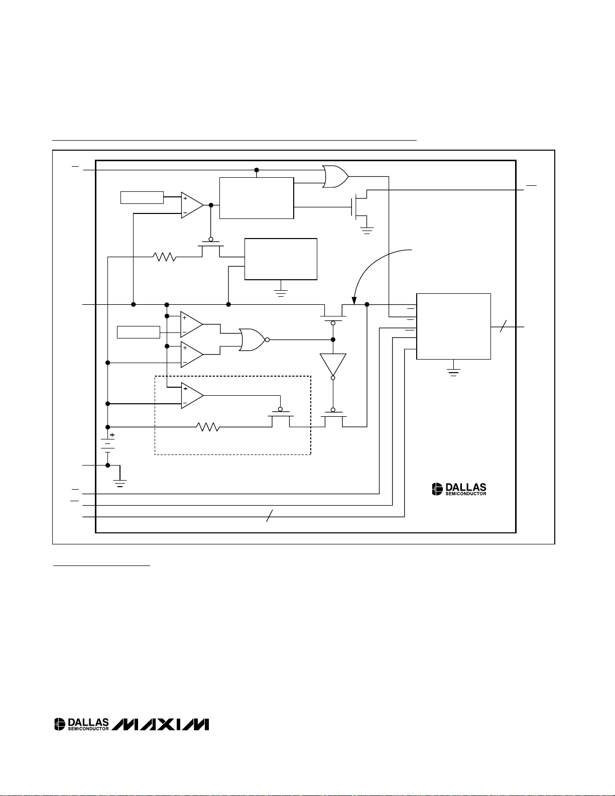
Functional Diagram
CURRENT-LIMITING
RESISTOR
BATTERY-CHARGING/SHORTING
PROTECTION CIRCUITRY (UL RECOGNIZED)
REDUNDANT LOGIC
DELAY TIMING
CIRCUITRY
CHARGER
CURRENT-LIMITING
RESISTOR
V
TP
REF
V
SW
REF
GND
ML
CE
RST
CE
REDUNDANT
SERIES FET
SRAM
DQ0–7
OE
WE
V
CC
V
CC
UNINTERRUPTED
POWER SUPPLY
FOR THE SRAM
DS2045W
OE
WE
A0–A16
Detailed Description
The DS2045W is a 1Mb (128kb x 8 bits) fully static, NV
memory similar in function and organization to the
DS1245W NV SRAM, but containing a rechargeable ML
battery. The DS2045W NV SRAM constantly monitors
VCCfor an out-of-tolerance condition. When such a condition occurs, the lithium energy source is automatically
switched on and write protection is unconditionally
enabled to prevent data corruption. There is no limit to
the number of write cycles that can be executed and no
additional support circuitry is required for microprocessor
interfacing. This device can be used in place of SRAM,
EEPROM, or flash components.
The DS2045W assembly consists of a low-power SRAM,
an ML battery, and an NV controller with a battery charger, integrated on a standard 256-ball, 27mm2BGA substrate. Unlike other surface-mount NV memory modules
that require the battery to be removable for soldering,
the internal ML battery can tolerate exposure to convection reflow soldering temperatures allowing this single-piece component to be handled with standard BGA
assembly techniques.
The DS2045W also contains a power-supply monitor
output, RST, which can be used as a CPU supervisor
for a microprocessor.

DS2045W
Read Mode
The DS2045W executes a read cycle whenever WE (write
enable) is inactive (high) and CE (chip enable) is active
(low). The unique address specified by the 17 address
inputs (A0 to A16) defines which of the 131,072 bytes of
data is to be accessed. Valid data will be available to the
eight data output drivers within t
ACC
(access time) after
the last address input signal is stable, providing that CE
and OE (output enable) access times are also satisfied. If
CE and OE access times are not satisfied, then data
access must be measured from the later occurring signal
(CE or OE) and the limiting parameter is either tCOfor CE
or tOEfor OE rather than address access.
Write Mode
The DS2045W executes a write cycle whenever the CE
and WE signals are active (low) after address inputs
are stable. The later-occurring falling edge of CE or WE
will determine the start of the write cycle. The write
cycle is terminated by the earlier rising edge of CE or
WE. All address inputs must be kept valid throughout
the write cycle. WE must return to the high state for a
minimum recovery time (t
WR
) before another cycle can
be initiated. The OE control signal should be kept inactive (high) during write cycles to avoid bus contention.
However, if the output drivers have been enabled (CE
and OE active) then WE will disable the outputs in t
ODW
from its falling edge.
Data-Retention Mode
The DS2045W provides full functional capability for V
CC
greater than 3.0V and write-protects by 2.8V. Data is
maintained in the absence of VCCwithout additional
support circuitry. The NV static RAM constantly monitors V
CC
. Should the supply voltage decay, the NV
SRAM automatically write-protects itself. All inputs
become “don’t care”, and all data outputs become high
impedance. As VCCfalls below approximately 2.5V
(VSW), the power-switching circuit connects the lithium
energy source to the RAM to retain data. During powerup, when VCCrises above VSW, the power-switching
circuit connects external VCCto the RAM and disconnects the lithium energy source. Normal RAM operation
can resume after VCCexceeds VTPfor a minimum
duration of t
REC
.
Battery Charging
When VCCis greater than VTP, an internal regulator
charges the battery. The UL-approved charger circuit
includes short-circuit protection and a temperature-stabilized voltage reference for on-demand charging of
the internal battery. Typical data-retention expectations
of 3 years per charge cycle are achievable.
A maximum of 96 hours of charging time is required to
fully charge a depleted battery.
System Power Monitoring
When the external VCCsupply falls below the selected
out-of-tolerance trip point, the output RST is forced
active (low). Once active, the RST is held active until
the VCCsupply has fallen below that of the internal battery. On power-up, the RST output is held active until
the external supply is greater than the selected trip
point and one reset timeout period (t
RPU
) has elapsed.
This is sufficiently longer than t
REC
to ensure that the
SRAM is ready for access by the microprocessor.
Freshness Seal and Shipping
The DS2045W is shipped from Dallas Semiconductor
with the lithium battery electrically disconnected, guaranteeing that no battery capacity has been consumed
during transit or storage. As shipped, the lithium battery
is ~60% charged, and no preassembly charging operations should be attempted.
When VCCis first applied at a level greater than VTP,
the lithium battery is enabled for backup operation. A
96 hour initial battery charge time is recommended for
new system installations.
DS2045W 3.3V Single-Piece 1Mb
Nonvolatile SRAM
10 ____________________________________________________________________
Memory Operation Truth Table
X = Don’t care.
WE CE OE MODE I
CC
OUTPUTS
100 Read Active Active
101 Read Active High Impedance
00XWrite Active High Impedance
X1X Standby Standby High Impedance

Recommended Cleaning Procedures
The DS2045W may be cleaned using aqueous-based
cleaning solutions. No special precautions are needed
when cleaning boards containing a DS2045W module.
Removal of the topside label violates the environmental integrity of the package and voids the warranty of
the product.
Applications Information
Power-Supply Decoupling
To achieve the best results when using the DS2045W,
decouple the power supply with a 0.1µF capacitor. Use
a high-quality, ceramic surface-mount capacitor if possible. Surface-mount components minimize lead inductance, which improves performance, while ceramic
capacitors have adequately high frequency response
for decoupling applications.
Using the Open-Drain
RST
Output
The RST output is open drain, and therefore requires a
pullup resistor to realize a high logic output level. Pullup
resistor values between 1kΩ and 10kΩ are typical.
Battery Charging/Lifetime
The DS2045W charges an ML battery to maximum
capacity in approximately 96 hours of operation when
VCCis greater than VTP. Once the battery is charged,
its lifetime depends primarily on the VCCduty cycle.
The DS2045W can maintain data from a single, initial
charge for up to 3 years. Once recharged, this deepdischarge cycle can be repeated up to 20 times, producing a worst-case service life of 60 years. More
typical duty cycles are of shorter duration, enabling the
DS2045W to be charged hundreds of times, therefore
extending the service life well beyond 60 years.
DS2045W
DS2045W 3.3V Single-Piece 1Mb
Nonvolatile SRAM
____________________________________________________________________ 11
Note: All temperatures refer to top side of the package, measured on the package body surface.
PROFILE FEATURE
Sn-Pb EUTECTIC
ASSEMBLY
Average ramp-up rate
(T
L
to TP)
3°C/second max
Preheat
- Temperature min (T
Smin
)
- Temperature max (T
Smax
)
- Time (min to max) (ts)
100°C
150°C
60 to 120 seconds
T
Smax
to T
L
- Ramp-up rate
Time maintained above:
-
Temperature (TL)
- Time (t
L
)
183°C
60 to 150 seconds
Peak temperature (TP) 225 +0/-5°C
Time within 5°C of actual peak
temperature (T
P
)
10 to 30 seconds
Ramp-down rate 6°C/second max
Time 25°C to peak temperature 6 minutes max
Recommended Reflow Temperature Profile
DS2045W
DS2045W 3.3V Single-Piece 1Mb
Nonvolatile SRAM
Maxim cannot assume responsibility for use of any circuitry other than circuitry entirely embodied in a Maxim product. No circuit patent licenses are
implied. Maxim reserves the right to change the circuitry and specifications without notice at any time.
12 ____________________Maxim Integrated Products, 120 San Gabriel Drive, Sunnyvale, CA 94086 408-737-7600
© 2005 Maxim Integrated Products Printed USA is a registered trademark of Maxim Integrated Products.
is a registered trademark of Dallas Semiconductor Corporation.
Package Information
For the latest package outline information, go to
www.maxim-ic.com/DallasPackInfo
.
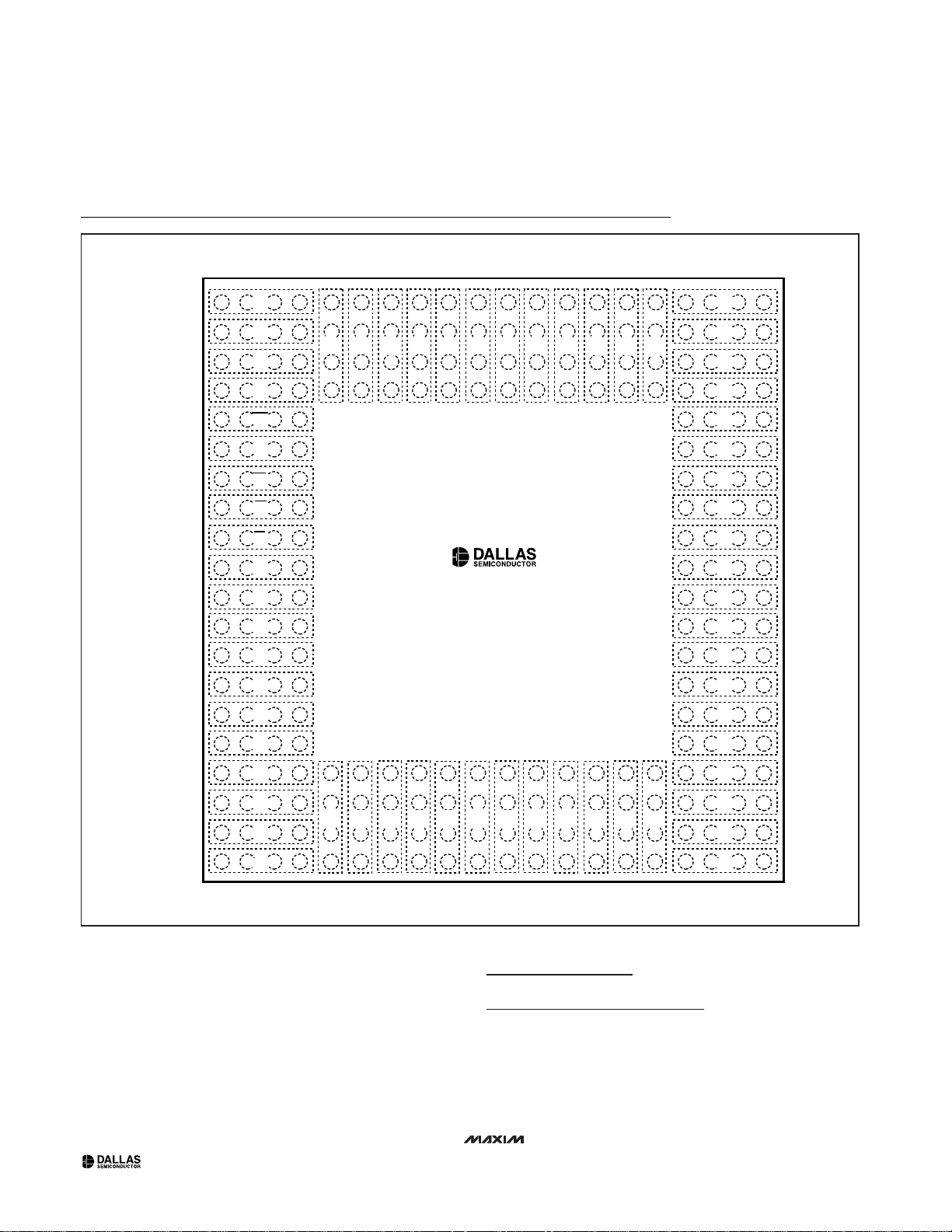
Pin Configuration
A
12
34
789
0
5
6
7
8
90
1
2
34
56
1
2
34 1
1
1
2
5
678
9
1
1
1
1
1
1
1
11
1
2
1
1
1
11
1
1
7
8
9
0
0
1
2
3
4
5
6
DS2045W
B
C
D
E
F
G
H
J
K
L
M
N
P
R
T
U
V
W
Y
A
B
C
D
E
F
G
H
J
K
L
M
N
P
R
T
U
V
W
Y
TOP VIEW
GND
N.C.
A15
A16
RST
V
CC
WE
OE
CE
DQ7
DQ6
DQ5
DQ4
DQ3
DQ2
DQ1
DQ0
GND
GND
GND
GND
N.C.
N.C.
A14
A13
A12
A11
A10
A9
A8
A7
A6
A5
A4
A3
A2
A1
A0
GND
GND
N.C.
N.C.
N.C.
N.C.
N.C.
N.C.
N.C.
N.C.
N.C.
N.C.
N.C.
N.C.
N.C.
N.C.
N.C.
N.C.
N.C.
N.C.
N.C.
N.C.
N.C.
N.C.
N.C.
N.C.
 Loading...