

Page 1
1-Wire is a registered trademark of Maxim Integrated Products, Inc.
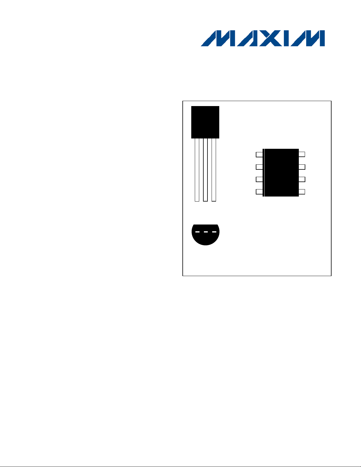
TO-92
1
(BOTTOM VIEW)
2
3
MAXIM
1
GND
DQ
V
2
3
SO (150 mils)
N.C.
N.C.
N.C.
N.C.
GND
DQ
VDD
N.C.
6 8 7 5 3
2
4
19-5474; Rev 8/10
DS18S20
Wire Digital Thermometer
High-Precision 1-
FEATURES
Unique 1-Wire® Interface Requ ires Only O ne
Port Pin for Co mmunic a tion
Each Device has a Unique 64-Bit Serial C ode
Stored i n an On-Board ROM
Multidrop Capability Simplifies Distributed
Temperature S ensing App lications
Requi res No External Compone nts
Can Be Powered from Data Line. Power
Supply Range is 3.0V to 5.5V
Measures Temperat ur es from -55°C to
+125°C (-67°F to +257°F)
±0.5°C Accuracy from -10°C to +85°C
9-B it Thermome ter Resolu tion
Converts Temperat ure in 750ms (max)
User-Definable Nonvolatile (NV) Alarm
Settings
Alarm Search Command Identifies and
Addresses Devices Who se T emperature is
Outside Programmed Lim its (T emperature
Al a rm C ondition )
Applications Include Thermostatic Controls,
Industrial Systems, Consumer Prod u cts,
PIN CONFIGURATIONS
DS1820
(DS18S20)
DD
(DS18S20Z)
DS1820
Thermometers, or Any Therma lly Sensit ive
System
DESCRIPTION
The DS18S20 digital thermometer provides 9-bit Celsius temperature measurements and has an alarm
function with nonvolatile user-programmable upper and lower trigger points. The DS18S20
communicates over a 1-Wire bus that by definition requires only one data line (and ground) for
communicat ion with a ce ntral micro pro cessor. It has an op erat ing temperat ure r ange of –55°C to +125°C
and is ac curat e to ±0.5°C over the range of –10°C to +85°C. In additio n, the DS18S20 can der ive power
directly from the data line (“parasite power”), eliminating the need for an external power supply.
Each DS18S20 has a unique 64-bit serial code, which allows multiple DS18S20s t o fu nc tion on t he s a me
1-Wire bus. Thus, it is simple to use one microprocessor to control many DS18S20s distributed over a
large area. Applications that can benefit from this feature include HVAC environmental controls,
temperature monitoring systems inside buildings, equipment, or machinery, and process monitoring and
contro l systems.
1 of 23
Page 2

DS18S20
PART
TEMP RANGE
PIN-PACKAGE
DS18S20
–55°C to +125°C
3 TO-92
DS18S20+
–55°C to +125°C
3 TO-92
DS18S20/T&R
–55°C to +125°C
3 TO-92 (2000 Piece)
DS18S20+T&R
–55°C to +125°C
3 TO-92 (2000 Piece)
DS18S20-SL/T&R
–55°C to +125°C
3 TO-92 (2000 Piece)*
DS18S20-SL+T&R
–55°C to +125°C
3 TO-92 (2000 Piece)*
DS18S20Z
–55°C to +125°C
8 SO
DS18S20Z+
–55°C to +125°C
8 SO
DS18S20Z/T&R
–55°C to +125°C
8 SO (2500 Piece)
DS18S20Z+T&R
–55°C to +125°C
8 SO (2500 Piece)
Data Input/Output. Open-dr ain 1-Wire interface pin. Also provides
Powering the DS18S20 section.)
Op tional VDD. VDD must be grounded for oper at ion in parasite
power mode.
1, 2, 6, 7,
ORDERING INFORMATION
+Denotes a lead(Pb)-free/RoHS-compliant package. A “+” appears on the top mark of le ad(Pb)-fr e e pac k a ges .
T&R = Tape and reel.
*TO-92 pack ages in ta pe and re el ca n be or der ed w ith s tra ight or fo rme d lea ds. Ch oos e “SL ” for s tra ight lea ds. B ulk TO -92 or de rs ar e s traigh t
leads only.
PIN DESCRIPTION
PIN
TO-92 SO
NAME FUNCTION
1 5 GND Ground
2 4 DQ
power to the device whe n used in parasite power mode (see the
3 3 VDD
—
8
N.C. No Connection
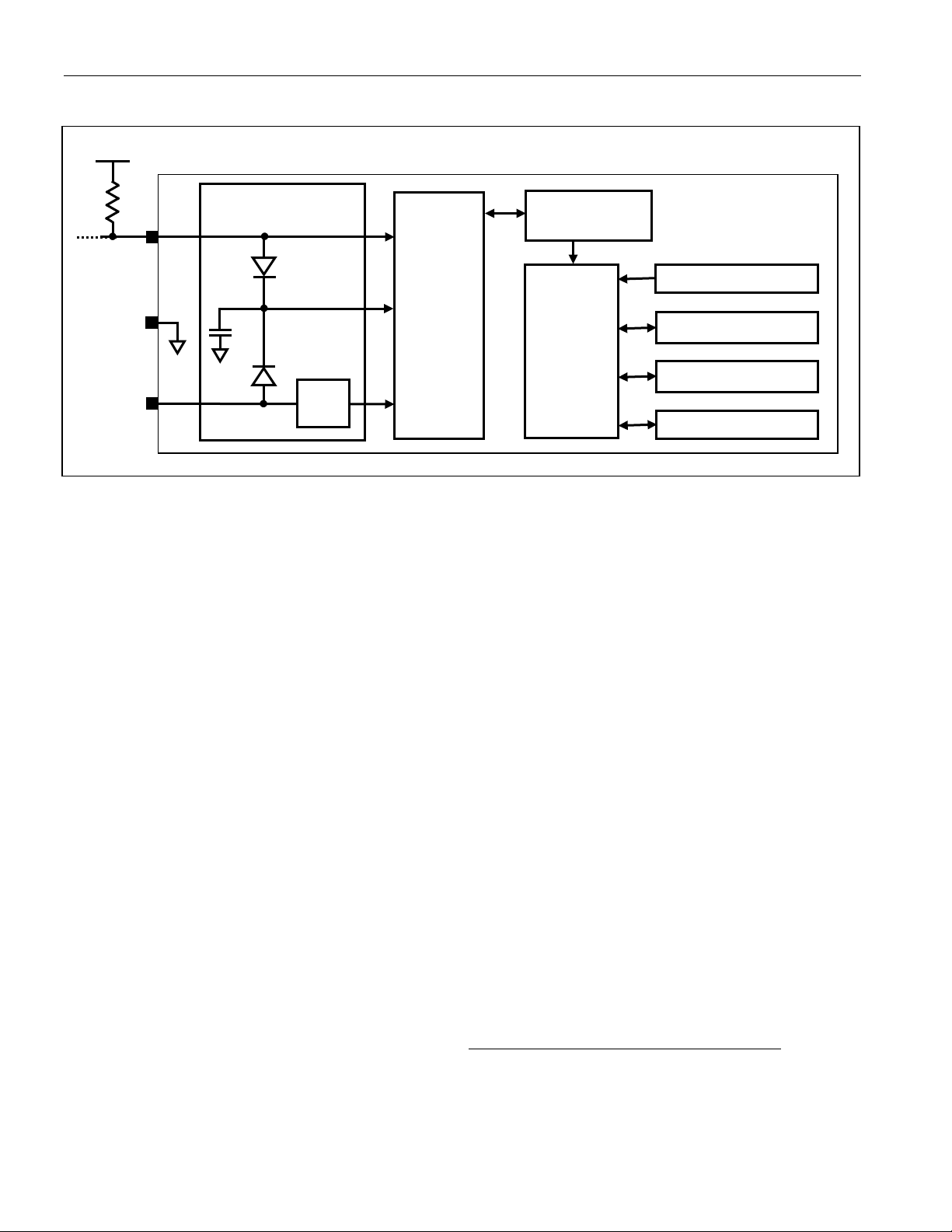
OVERVIEW
Figure 1 shows a block d iagram of the DS18S20, and pin descriptions are given in the Pin Description
table. The 64-bit RO M st ores the device’s un ique serial code. The scrat chpad memory contains t he 2 -byte
temperature r egister t hat stores t he digital ou tp ut from the te mperatur e sensor . In addition, t he scratchpad
provides access t o the 1-byte upper and lower alarm trigger registers (TH and TL). The TH and TL registers
are nonvolatile (EEP ROM), so they will retain data when the device is powered do wn.
The DS18S20 uses Maxim’s exclusive 1-Wire bus protocol that implement s bus communicat ion using
one control signal. The cont rol line requires a weak pullup res istor since all dev ices are linked to t he bus
via a 3-state or open-drain port (the DQ pin in the case of the DS18S20). In this bus system, the
microprocesso r (the master dev ice) identifies and addresses devices on the bus using each device’s unique
64-bit code. Because each device has a unique co de, the number of devices t hat can be addressed on one
bus is virtually unlimited. The 1-Wire bus protocol, including detailed explanations of the commands and
“time slots,” is covered in the 1-Wire Bus System section.
Another feature of the DS18S20 is the ability to operate without an external power supply. Power is
instead supplied through the 1-Wire pullup resist or via the DQ pin when the bus is high. The high bus
signal also charge s an internal capacito r (CPP), whic h the n sup plie s po wer to the de vic e whe n the bus is
low. This method of deriving power from the 1-Wire bus is referred to as “parasite power.” As an
alt ernative , t he DS1 8S20 may als o be p owe red by an e xternal supply on VDD.
2 of 23
Page 3
DS18S20
CPERCOUNT
REMAINCOUNTCPERCOUNT
READTEMPETEMPERATUR
__
___
25.0_
−
+−=
VPU
64-BIT ROM
DQ
VDD
INTERNAL VDD
CPP
PARA SITE POWER
CIRCUIT
MEMORY CONTROL
LOGIC
8-BIT CRC GENERATOR
TEMPER ATUR E SENS OR
ALARM HIGH TRIGGER (TH)
ALARM LOW TRIGGER (TL)
GND
DS18S20
Figure 1. DS18S20 Block Diagram
4.7k
POWERSUPPLY
SENSE
AND
1-Wire PORT
SCRATCHPAD
REGISTER (EEPROM)
REGISTER (EEPROM)
OPERATION—MEASURING TEMPERATURE
The core funct ionality of the DS18S20 is its direct -to-digital temperatu re sensor. The t emperature sensor
out put has 9-bit resolution, which corresponds to 0.5°C steps. The DS18S20 powers-up in a lo w-power
idle stat e; to initiat e a t emperat ure measurement and A-to-D co nver s ion, the mast e r mu st issu e a Co nve rt
T [44h] command. Following the conversion, the resulting thermal data is stored in the 2-byte
temperature r egister in the scrat chpad memory a nd the DS18S20 returns to its idle state. If the DS18S20
is powered by an external supply, the master can issue “read-time slots” (see the 1-Wire Bus System
section) after the Convert T command and the DS18S20 will respond by transmitting 0 while the
temperature conversion is in progress and 1 when the convers io n is do ne. If the DS18S20 is power ed wit h
parasite power , this notification technique cannot be used since the bus must be pulled high by a strong
pullup during the entire temperatur e co nversion. T he bus requirements for par asite power are explained in
detail in the Powering the DS18S20 section.
The DS18S20 output d ata is calibrat ed in degrees cent igrade; for Fa hrenheit appl ications, a lookup t able
or conversion routine must be used. The temperature data is stored as a 16-bit sign-extended two’s
complement number in the temperature register (see Figure 2). The sign bits (S) indicate if the
temperature is po sitive or negative: for positive nu mbers S = 0 and for negative numbers S = 1. Table 1
gives examples of digital output data and the corresponding temperature reading.
Resolutions great er t han 9 bit s can be ca lculat ed using t he dat a fro m the t e mperature, COUNT RE MAIN
and COUNT PER °C registers in the scratchpad. Not e that the COUNT PER °C register is hard-w ire d t o
16 (10h). After reading the scratchpad, the TE MP_R EAD va lue is obt ained by t runcat ing t he 0. 5°C b it
(bit 0) from the temperature data (see Figure 2). The extended resolution temperature can then be
calculated using the fo llowing equation:
3 of 23
Page 4

Figure 2. Temper atu re Register Form at
BIT 7
BIT 6
BIT 5
BIT 4
BIT 3
BIT 2
BIT 1
BIT 0
LS B YTE
BIT 15
BIT 14
BIT 13
BIT 12
BIT 11
BIT 10
BIT 9
BIT 8
MS BYTE
+85.0*
0000 0000 1010 1010
00AAh
+0.5
0000 0000 0000 0001
0001h
0
0000 0000 0000 0000
0000h
-0.5
1111 1111 1111 1111
FFFFh
-25.0
1111 1111 1100 1110
FFCEh
-55.0
1111 1111 1001 0010
FF92h
BIT 7
BIT 6
BIT 5
BIT 4
BIT 3
BIT 2
BIT 1
BIT 0
26 25 24 23 22 21 20 2-1
S S S S S S S S
S = SIGN
Table 1. Temperatu r e/Data Relation sh ip
DS18S20
TEMPERATURE
(°C)
DIGITAL OUTPUT
(BINARY)
DIGITAL OUTPUT
(HEX)
+25.0 0000 0000 0011 0010 0032h
*The power-on reset value of the temperature register is +85°C.
OPERATION—ALARM SIGNALING
After the DS18S20 p erforms a temperature co nversion, the temperature value is co mpared to t he userdefined two’s complement alarm trigger values sto red in the 1-byt e T
The s ig n bit (S)
ind icates if the va lu e is po s itive o r negat ive : for positive numbers S = 0 and for negative
numbers S = 1. The TH and TL registers are nonvolatile (EEPROM) so they will retain data when the
device is powered do wn. TH and TL can be accessed t hrough bytes 2 and 3 o f the scratchpad a s exp lained
in the Memory section.
Figure 3. T
and TL Register Format
H
a nd TL reg isters (see Figure 3).
H
S 26 25 25 25 22 21 20
Only bits 8 through 1 o f the temperat ure register are used in the TH and TL compar iso n sinc e TH and T
are 8-bit regist ers. If the measured t emperature is low er t han o r eq ual t o TL o r h igher tha n TH, an alarm
condition exists and an alarm flag is set inside the DS18S20. This flag is updated after every temperature
measurement; therefore, if the alarm condition goes away, the flag will be turned off after the next
temperature convers io n.
The master device can ch eck the alarm flag status of all DS18S20s o n t he bus by issuing an Alarm Search
[ECh] command. Any DS18S20 s with a set alarm flag will respond to the command, so the master can
determine exactly which DS18S20s have experienced an alarm co nd it io n. I f an alar m co nd it io n e xist s and
the TH or TL s ett ing s ha ve c ha nged , a no the r t empe r at ure conve r sio n sho u ld be do ne t o valid at e t he ala r m
condition.
4 of 23
L
Page 5

DS18S20
POWERING THE DS18S20
The DS18S20 can be powered by an external supply on the VDD pin, or it can operate in “parasite power”
mode, which allows the DS18S20 to function without a local external supply. Parasite power is very
useful for applications that require remote temperature sensing or those with space constraints.
Figure 1 shows the DS18S20’s parasite-power contro l circuitry, which “st eals” power from the 1-Wire
bus via the DQ pin when the bus is high. The stolen charge powers the DS18S20 while the bus is high,
and some o f the charge is sto red on the paras ite po wer capacitor ( CPP) to provide power when the bus is
low. When the DS18S20 is used in parasite po wer mode, t he VDD pin must be connec ted to gr ound .
In parasite power mode, the 1-Wire bus and CPP can provide sufficient current to the DS18S20 for most
operations as long as the specified timing and voltage requirements are met (see the DC Electrical
Characteristics and the AC Electrical Characteristics). However, when the DS18S20 is performing
temperature convers ions or copying dat a fro m the scratchpad memory to EE PROM, the operat ing current
can be as hig h as 1.5mA. This curre nt can cause an u nacceptable voltage dr op across the weak 1-Wire
pullup resisto r and is more current than can be supplied by CPP. To assur e that t he DS18S 20 has sufficient
supply current, it is necessary to provide a strong pullup on the 1-Wire bus whenever temperature
conversions are taking place or data is being copied from the scratchpad to EEPROM. This can be
accomplished by u sing a MOSFET to pull the bus d ire ctly t o the r ail a s s hown in Figure 4. The 1-Wire
bus must be switched to the strong pullup within 10µs (max) after a Convert T [44h] or Copy Scratchpad
[48h] command is issued, and the bus must be held high by the pullup for the durat ion of the conversion
(t
) or data transfer (tWR = 10ms). No ot her activity ca n take place on t he 1-Wire bus w h ile t he pullup
CONV
is enabled .
The DS18S20 can also be power ed by the conventional method of connect ing an external power supp ly to
the VDD pin, as shown in Figure 5. The advantage of this method is that the MOSFET pullup is not
required, and the 1-Wire bus is free t o car r y other traffic during the temperature co nversion t ime.
The use of parasite po wer is not reco mmended for temperatures above 100°C s ince t he DS18S20 may not
be able to sust ain communicat ions due t o the higher leakage curr ents t hat can exist at these te mperatures.
For applicat ions in which su ch te mperatures are like ly, it is st rongly reco mmended that t he DS18S2 0 be
powered by an external power supply.
In so me sit ua t ions t he bu s ma st e r ma y no t kno w whe t her t he DS 18 S2 0s o n t he bu s are par a sit e po w er ed
or po we red by ext er nal sup p lies. T he mas te r nee ds th is in for mat io n to det er mine if t he st r ong bus p u llup
should be used during temperature conversions. To get this infor mat ion, t he master can issue a Sk ip RO M
[CCh] command followed by a Read Power Supply [B4h] command followed by a “read-time slot”.
During the read-time slot, parasite powered DS18S20s will pull the bus low, and externally powered
DS18S20s will let the bus remain high. If the bus is pulled low, the master knows t hat it must supply the
strong pullup on the 1-Wire bus during temperature conversions.
5 of 23
Page 6

DS18S20
8-BIT CRC
48-BIT SERIAL NUMBER
8-BIT FAMILY CODE (10h)
VPU
VPU
4.7k
1-Wire BUS
P
DS18S20
GND
VDD
DQ
TO OTHER
1-WIRE DEVICES
VDD (EXTERNAL SUPPLY)
DS18S20
GND
VDD
DQ
VPU
4.7k
TO OTHER
1-WIRE DEVICES
1-Wire BUS
P
MSB
MSB
LSB
LSB
LSB
MSB
Figure 4. Supplying the Parasite-Power ed DS18S 20 During Temperature Conversions
µ
Figure 5. Powering the DS18S20 with an External Supply
µ
64-BIT LASERED ROM CODE
Each DS18S20 contains a unique 64-bit code (see Figure 6) st or ed in ROM. Th e least significant 8 b its of
the ROM code co ntain the DS18S20’s 1-Wire family code: 10h. The next 48 bits contain a unique serial
numb er. The most signif ica nt 8 bits contain a cyclic redundancy check (CRC) byte that is calculat ed from
the first 56 bits of the ROM code. A detailed explanation of the CRC bits is provided in the CRC
Generation section. The 64-bit ROM code and associated ROM function control logic allow the
DS18S20 to operate as a 1-Wire device using the protocol detailed in the 1-Wire Bu s S yst e m section.
Figure 6. 64-Bit Lasered ROM Code
6 of 23
Page 7

DS18S20
SCRATCHPAD
(POWER-UP STATE)
*
(85°C)
MEMORY
The DS18S20’s memory is organized as shown in Figure 7. The memory consists of an SRAM
scratchpad wit h nonvolatile EEPROM stor age for the high and low alarm t rigger reg isters (TH and TL).
Note that if the DS18S20 alar m fu nction is not used, the TH and TL register s can serve as ge ner al-purpose
memory. A ll memo ry commands are de s c ribed in de tail in the DS18S20 Function Commands section.
Byte 0 and byte 1 of the scratchpad contain the LSB and the MSB of the temperature register,
respectively. T hese b ytes are read-o nly. Bytes 2 and 3 provide access t o TH and TL reg isters. Bytes 4 and
5 are reserved for internal use by the device a nd ca nnot be over written; the se b ytes will retur n all 1s when
read. Bytes 6 a nd 7 conta in the COUNT REM AIN and CO UNT P ER ºC reg isters, w hich can be u sed to
calculate extended resolution results as explained in the Operation—Measuring Temperature section.
Byte 8 of the scrat chpad is read -o n ly and c o nt ains the C R C code for bytes 0 through 7 o f the scratchpad.
The DS18S20 generates this CRC using the method described in the CRC Generation section.
Data is written to bytes 2 and 3 of the scratchpad using the Write Scrat chpad [4Eh] command; the data
must be transmitted to the DS18S20 starting with the least significant bit of byte 2. To verify data
integrity, the scratchpad can be read (using the Read Scratchpad [BEh] command) after the data is
written. When reading the scratchpad, data is transferred over the 1-Wire bus starting with the least
significant bit o f byt e 0. To transfer the TH and TL dat a fro m the scratchpad to EE P ROM, t he mast er must
issue the Copy Scratchpad [48h] command.
Data in the EEP ROM register s is retained w hen the device is powered do wn; at po wer-up the EEPROM
data is reload ed into the co r r esponding scratchpad locations. Data can also be reloaded from EE P ROM to
the scratchpad at any time using the Recal l E2 [B 8h] co mmand . The master can issue “read-time slot s”
(see the 1-Wire Bu s Sy stem section) fo llowing the Reca ll E2 command and the DS18S20 will indicate the
status of the recall by transmitting 0 while the recall is in progress and 1 when the reca ll is done.
Figure 7. DS18S20 Memory Ma p
Byte 0 Temperature LSB (AAh)
Byte 1 Temperature MSB (00h)
EEPROM
Byte 2 TH Register or User Byte 1* TH Register or User Byte 1
Byte 3 TL Register or User Byte 2* TL Register or User Byte 2
Byte 4 Reserved (FFh)
Byte 5 Reserved (FFh)
Byte 6 COUNT REMAIN (0Ch)
Byte 7 COUNT PE R °C (1 0h)
Byte 8 CRC*
Power-up state depends on value(s) stored in EEPROM.
7 of 23
Page 8

DS18S20
XOR
INPUT
CRC GENERATION
CRC bytes are provided as part of the DS18S20’s 64-bit ROM code and in the 9th byte o f the scrat chpad
memory. The ROM code CRC is calculat ed from the first 56 bits of the ROM code and is co nt ained in t he
most significant byte of the ROM. The scratchpad CRC is calculated from the data stored in the
scratchpad, and there fore it changes w hen the data in the scratchpad c hanges. The CRCs pro vide the bu s
master with a method of data validation when data is read from the DS18S20. To ver ify that data has been
read corr ectly, the bus maste r must re-calculate the CRC fro m the received data a nd then compare t his
value to either t he ROM code CRC ( for ROM rea ds) or to the scratchpad CRC ( for scratchpad r eads). I f
the calculated CRC mat ches the read CRC, t he dat a ha s bee n rec eived error free. The comparison of CRC
values and t he dec ision to co ntinue w ith an o peratio n are det er mined ent irely b y t he bus ma ster . T here is
no circuitry inside the DS18S20 that prevents a command sequence from proceeding if the DS18S20
CRC (ROM or scr at c hpad) does not match the value generat ed by the bus master .
The e quivale nt polynomial function of the C RC (R O M or sc ratchpa d) is:
CRC = X8 + X5 + X4 + 1
The bus master can re-calculate the CRC and compare it to the CRC values from the DS18S20 using the
po lynom ial g ener at or sho wn in Figure 8. This circuit consists o f a shift register and XOR gates, and the
shift register b its are initialized t o 0. Start ing with the least signif icant bit of the ROM code or the least
significant bit of byte 0 in the scratchpad, one bit at a time shou ld shifted into t he shift regist er. After
shifting in the 56th bit from the ROM or the most significant bit of byte 7 from the scratchpad, the
po lynom ial g ener at or w ill co nta in the re-ca lculated CRC. Next , the 8-bit R OM code o r scratchpad CRC
from the DS18S20 must be shifted into the circuit. At this point, if the re-calculated CRC was correct, the
shift register w ill co nta in all 0s. Add itio nal in format ion about the Ma xim 1-Wire cyclic redundancy check
is a vailab le in Application Note 27: Understanding and Using Cyclic Redundancy Checks with Maxim
iButton Products.
Figure 8. CRC Generator
(MSB) (LSB)
XOR XOR
8 of 23
Page 9
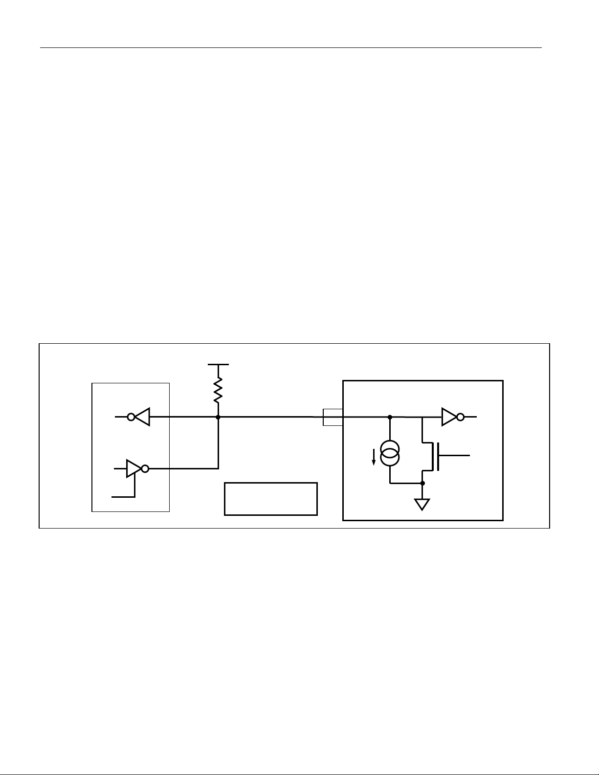
DS18S20
VPU
4.7k
5μA
Rx
Tx
DS18S20 1-Wire PORT
100Ω
MOSFET
TX
Rx
Rx = RECEIVE
Tx = TRANSMIT
1-Wire BUS
DQ
1-WIRE BUS SYSTEM
The 1-Wire bus system uses a s ingle bus master to control one or more slave devices. T he DS18S20 is
always a slave. When there is only one slave on the bus, the system is referred to as a “single-drop”
system; the s ys te m is “ multidrop” if there are multiple slaves on the bus .
All data and commands are tr ansmitted least significant bit first over the 1-Wire bus.
The following discussion of the 1-Wire bus system is broken down into three topics: hardware
configuration, t r ansaction sequence, and 1-Wire signaling (signal types and timing).
HARDWARE CONFIGURATION
The 1-Wire bu s has by de finition only a single da ta line. Each device ( master or slave) inter faces to the
data line via an open dra in or 3-stat e port. This allows each de vice to “release” the dat a line when t he
dev ice is no t t rans mitt ing d at a so the bus is a vail able for use by a not her device. The 1-Wire port o f the
DS1 8S20 (t he DQ pin) is o pen drain wit h an interna l circuit equivalent t o tha t sho wn in Figure 9.
The 1-Wire bus requires an external pullup resistor of approximately 5kΩ; thus, the idle state for the
1-Wire bu s is high. If for any reason a transaction needs to be suspended , t he bus MU ST be left in the id le
state if the transact ion is to resume. Infin ite recovery time can occur bet ween bits so long as the 1-Wire
bus is in the inact ive (high) stat e during the reco very period. I f the bus is held low for more than 480µs,
all c ompone nts on the bus wi ll be reset.
Figure 9. Hardware Configuration
PIN
TYP
9 of 23
Page 10

DS18S20
TRANSACTION SEQUENCE
The transact ion sequence for access ing the DS18S20 is as follows:
Step 1. Initialization
Step 2. ROM Command (fo llowed by a ny requ ired data exchange)
Step 3. DS18S20 Function Command (followed by any required data exchange)
It is very important to follow this s e quence every t ime the DS18S20 is accessed, as the DS18S20 w il l not
respond if a ny steps in the seque nce are missing o r out of order. Except ions to this rule are the Se arch
ROM [F0h] and Alarm Search [ECh] commands. After issuing either of these ROM commands, the
master must return to Step 1 in the sequence.
INITIALIZATION
All transactions on the 1-Wire bus begin with an initialization sequence. The initialization sequence
consists of a reset p ulse transmitted by the bus master followed by presence pulse(s) t ransmitted by the
slave(s). The prese nc e pulse lets the bus ma ster know t hat s lave devices ( such as the DS18S20) ar e o n t he
bus and are read y t o op erate. Timing for t he reset and pre sence pu lses is det ailed in t he 1-Wire Sign aling
section.
ROM COMMANDS
After the bus master has detected a presence pulse, it can issue a ROM command. These commands
operate on the unique 64-bit ROM cod es of each slave device and allow the mast er to s ingle out a specific
device if many are present on the 1-Wire bus. These co mmands also a llow t he ma ste r to d etermin e ho w
many and what types of devices are present on the bus or if any device has experienced an alarm
condition. There are five ROM co mmands, and e ach command is 8 b its long. T he master device must
issue an appropriate ROM command before issuing a DS18S20 function command. A flowchart for
op eration o f the ROM commands i s shown in Figure 14.
SEARCH ROM [F0h]
When a system is in itially powered u p, the master must identify the ROM co des of all slave de vices on
the bus, which allows the master to determine the number of slaves and their device types. The master
learns the ROM codes through a process of elimination that requires the master to perform a Search ROM
cycle (i.e., S earch ROM co mmand fo llowed by da t a exchange) as many t imes as neces sary to ident ify all
of the slave dev ices. If there is only o ne slave on t he bus, the simp ler Read ROM co mmand (see below)
can be used in place of the Search ROM process. For a detailed explanation of the Search ROM
procedure, refer to the iButton® Book of Standards at www.maxim-ic.com/ibuttonbook. After every
Search ROM cycle, the bus master must return to Step 1 (Initialization) in the transaction sequence.
READ ROM [33h]
This command ca n only be used when there is one s lave on the bu s. It allows the bus ma ster to r ead the
sla ve’ s 64 -bit ROM code w ithout using the Search ROM procedure. If this command is used when there
is more than one slave present on the bus, a data collision will occur when all the slaves attempt to
respond at the same time.
MATCH ROM [55h]
The match ROM command fo llowed by a 64-bit ROM code sequence a llows the bus master to address a
spec ific sla ve dev ice on a multidr op or s ingle-drop bus. Only the slave t hat exactly matches the 64-bit
ROM code sequence will respo nd to the function command issued by the master ; all other slaves on the
bus will wait for a reset pulse.
iButton is a registered trademark of Maxim Integrated Products, Inc.
10 of 23
 Loading...