

Page 1
DS18B20
Programmable Resolution
Wire Digital Thermometer
TO-92
1
(BOTTOM VIEW)
2
3
MAXIM
1
GND
DQ
V
2
3
SO (150 mils)
N.C.
N.C.
N.C.
N.C.
GND
DQ
VDD
N.C.
6 7 3
MAXIM
18B20
N.C.
VDD
N.C.
N.C.
GND
N.C.
DQ
6
2
18B20
µSOP
1-Wire is a registered trademark of Maxim Integrat ed Pr o duc ts , Inc .
1-
DESCRIPTION
The DS18B20 digital thermometer provides 9-bit
to 12-bit Celsius temperature measurements and
has an alarm function with nonvolatile userprogrammable upper and lower trigger points.
The DS18B20 communicates over a 1-Wire bus
that by definition requires only one data line (and
ground) for communication with a central
microprocessor. It has an operating temperature
range of -55°C to +125°C and is accurate to
±0.5°C over the range of -10°C to +85°C. In
ad d it io n, t h e DS18B20 can derive power directly
from the data line ( “parasite power”) , eliminat ing
the need for an external power supply.
Each DS18B20 has a unique 64-bit serial code,
which allows multiple DS18B20s to function on
the same 1-Wir e bu s. Thu s , it is simple to us e one
microprocessor to control many DS18B20s
distributed over a large area. Applications that
can benefit from this feature include HVAC
environmental controls, temperature monitoring
systems inside buildings, equipment, or
machinery, and process monitoring and control
systems.
FEATURES
Unique 1-Wire® Interface Requires Only One
Port Pin for Communication
Each Device has a Unique 64-Bit Serial Code
Stor ed i n an On-Board ROM
Multidrop Capability Simplifies Distributed
Temperature-Sensing Applications
Requires No External Components
Can Be Powered from Data Line; Power Supply
Range is 3.0V to 5.5V
Measures Temperatures from -55°C to +125°C
(-67°F to +257°F)
±0.5°C Accuracy from -10°C to +85°C
Thermometer Resolution is User Selectable
from 9 to 12 Bits
Converts Temperature to 12-Bit Digital Word in
750ms (Max)
1 of 22 REV: 042208
User-Definable Nonvolatile (NV) Alarm
Settings
Alarm Search Command Identifies and
Addresses Devices Whose Temperature is
Outside Programmed Limits (Temperature
Alarm Condition)
Available in 8-Pin SO (150 mils), 8-Pin µSOP,
and 3-Pin TO-92 Packages
Software Compatible with the DS1822
Applications Include Thermostatic Controls,
Industrial Systems, Consumer Products,
Thermometers, or Any Thermally Sensitive
System
PIN CONFIGURATIONS
18B20
(DS18B20)
DD
2
(DS18B20Z)
3
(DS18B20U)
7
N.C.
Page 2

ORDERING INFORMATION
PART
TEMP RANGE
PIN-PACKAGE
TOP MARK
-55°C to +125°C
3 TO-92
DS18B20+
-55°C to +125°C
3 TO-92
18B20
DS18B20/T&R
3 TO-92 (2000 Piece)
18B20
DS18B20+T&R
3 TO-92 (2000 Piece)
18B20
DS18B20-SL/T&R
-55°C to +125°C
3 TO-92 (2000 Piece)*
18B20
DS18B20-SL+T&R
-55°C to +125°C
3 TO-92 (2000 Piece)*
18B20
DS18B20U
-55°C to +125°C
8 µSOP
18B20
DS18B20U+
-55°C to +125°C
8 µSOP
18B20
DS18B20U/T&R
-55°C to +125°C
8 µSOP (3000 Piece)
18B20
DS18B20U+T&R
-55°C to +125°C
8 µSOP (3000 Piece)
18B20
-55°C to +125°C
8 SO
DS18B20Z+
-55°C to +125°C
8 SO
DS18B20
DS18B20Z/T&R
-55°C to +125°C
8 SO (2500 Piece)
DS18B20
DS18B20Z+T&R
8 SO (2500 Piece)
DS18B20
µ
DS18B20
DS18B20
18B20
-55°C to +125°C
-55°C to +125°C
DS18B20Z
DS18B20
-55°C to +125°C
+Denotes a lead-fr ee p ac k age. A “+” will appear on the top mark of lead-free packages.
T&R = Tape and reel .
*TO-92 packa ges in tape an d re el ca n be or der ed w ith s tra ight or f o rmed leads . Ch oose “SL” for st raig ht leads. Bulk T O -92 or de rs ar e s traigh t
leads only.
PIN DESCRIPTION
SO
PIN
SOP
TO-92
NAME FUNCTION
1, 2, 6,
7, 8
3 8 3 VDD
2, 3, 5,
6, 7
— N.C. No Connection
Op tio nal VDD. VDD must be grounded for operation in
parasite power mode.
Data Input/Output. Ope n-drain 1-Wire interface pin. Also
4 1 2 DQ
provides power to the device when used in parasite power
mode (see the Powering the DS18B20 section.)
5 4 1 GND Ground
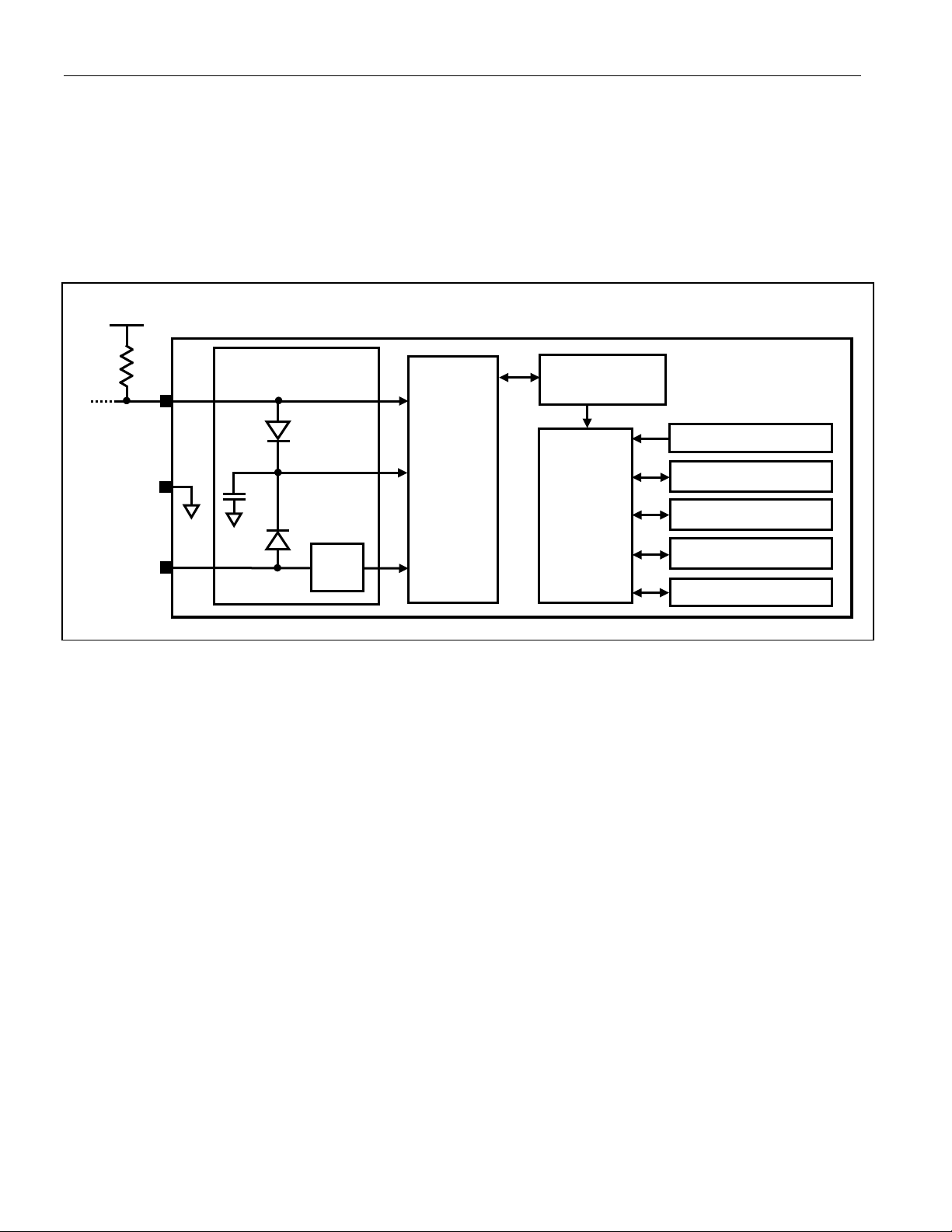
OVERVIEW
Figure 1 s hows a block diagram of the DS18B20, and pin descr iptions are given in the Pin De scription
table. The 64-bit ROM stores the device’s unique ser ial code. The scratchpad memor y contains the 2-byte
temperature r egister t hat stores t he digital ou tp ut from the te mperatur e sensor . In add ition, t he scratchpad
provides access to the 1-byte upper and lower alarm trigger registers (TH and TL) and the 1-byte
configuration reg ister. The co nfiguration register allows the user to set the resolut ion of the temperat ureto-digital conversion to 9, 10, 11, or 12 bits. The TH, TL, and configuration registers are nonvolatile
(EEPROM), so they will retain data when the device is powered down.
The DS18B20 uses Maxim’s exclusive 1-Wire bus p rotoco l that impleme nts bus commu nicat ion u sing
one control signal. The cont rol line requires a weak pullup res istor since all dev ices are linked to t he bus
via a 3-state or open-drain port (the DQ pin in the case of the DS18B20). In this bus system, the
microprocesso r (the master dev ice) identifies and addresses devices on the bus using each de vice’s unique
64-bit code. Because each device has a unique co de, the number of devices that can be addressed on one
2 of 22
Page 3
DS18B20
VPU
4.7k
64-BIT ROM
DQ
VDD
INTERNAL VDD
CIRCUIT
MEMORY CONTROL
LOGIC
SCRATCHPAD
8-BIT CRC GENERATOR
ALARM HIGH TRIGGER (TH)
ALARM LOW TRIGGER (TL)
CONFIGURATION REGISTER
GND
DS18B20
bus is virtually unlimited. The 1-Wire bus protocol, including detailed explanations o f the commands and
“time slots,” is covered in the 1-Wire Bus System section.
Another feature of the DS18B20 is the ability to operate without an external power supply. Power is
instead supplied through the 1-Wire pullup resistor via the DQ pin when the bus is high. The high bus
signal also charges an internal capacito r (CPP), whic h the n sup plie s po wer to the de vic e whe n the bus is
low. This method of deriving power from the 1-Wire bus is referred to as “parasite power.” As an
alt ernative, the DS18B20 may also be powered by a n external sup ply on VDD.
Figure 1. DS18B20 Block Diagram
PARA SITE POWER
CPP
POWERSUPPLY
SENSE
AND
1-Wire PORT
TEMPER ATUR E SENS OR
REGISTER (EEPROM)
REGISTER (EEPROM)
(EEPROM)
OPERATION—MEASURING TEMPERATURE
The core funct ionality o f the DS18B20 is its dire ct-to-digita l temperatu re sensor. The resolution of the
temperature sensor is user-configurable to 9, 10, 11, or 12 bits, corresponding to increments of 0.5°C,
0.25°C, 0.125°C, and 0.0625°C, respectively. The default resolution at power-up is 12-bit. The DS18B20
powers up in a low-power idle state. To initiate a t emperature measurement and A-to-D conve rsio n, the
master must issue a Convert T [44 h] command. Following the co nversion, the result ing t hermal data is
stored in the 2-byte t emperature register in the scratchpad memory and the DS18B20 returns to its idle
state. If the DS18B20 is powered by an e xter nal s upply, the master can issue “read time slots” (see the
1-Wire Bus S yst em section) after the Convert T command and the DS18B20 will respond by tr ansmitting
0 while the t emperature co nversion is in pr ogress and 1 whe n t he c o nver sio n is do n e. If the DS18B20 is
powered with parasite power, this notification technique cannot be used since the bus must be pulled high
by a st r ong pu llup dur ing the e nt ire te mperatur e conversion. T he bus requ irements for par asite pow er are
explained in d etail in the Powering the DS18B20 section.
The DS18B20 output temperature data is calibrated in degrees Celsius; for Fahrenheit applications, a
lookup table or conversion rout ine must be used. The t emperat ure data is sto red as a 16-b it sign-extended
two’s complement number in the temperature register (see Figure 2). The sign bits (S) indicate if the
temperature is po sitive or negat ive: for po sitive nu mbers S = 0 and for negat ive numbers S = 1. If the
DS18B20 is configured for 12-bit resolut ion, a ll bits in the temperature reg ister w ill contain valid data.
For 11-bit resolution, bit 0 is undefined. For 10-bit reso lution, bits 1 and 0 are undefined, and for 9-bit
resolution bits 2, 1, and 0 are undefined. Table 1 gives examples of digital output data and the
correspond ing temperature reading for 12-bit resolution conver sions.
3 of 22
Page 4

Figure 2. Temperature Register Format
BIT 7
BIT 6
BIT 5
BIT 4
BIT 3
BIT 2
BIT 1
BIT 0
BIT 15
BIT 14
BIT 13
BIT 12
BIT 11
BIT 10
BIT 9
BIT 8
BIT 7
BIT 6
BIT 5
BIT 4
BIT 3
BIT 2
BIT 1
BIT 0
DS18B20
LS B YTE
MS BYTE
S = SIGN
3
22 21 20 2-1 2-2 2-3 2-4
2
S S S S S 2
Table 1. Temperature/Data Relationship
TEMPERATURE (°C)
DIGITAL O U TPUT
(BINARY)
+125 0000 0111 1101 0000 07D0h
+85* 0000 0101 0101 0000 0550h
+25.0625 0000 0001 1001 0001 0191h
+10.125 0000 0000 1010 0010 00A2h
+0.5 0000 0000 0000 1000 0008h
0 0000 0000 0000 0000 0000h
-0.5 1111 1111 1111 1000 FFF8h
-10.125 1111 1111 0101 1110 FF5Eh
DIGITAL OUTPUT
(HEX)
6
25 24
-25.0625 1111 1110 0110 1111 FE6Fh
-55 1111 1100 1001 0000 FC90h
*The power-on reset value of the temperature register is +85°C.
OPERATION—ALARM SIGNALING
After the DS18B20 performs a temperature conversion, the t emperature value is compared to the userdefined two’s complement alarm trigger values sto red in the 1-byt e TH and TL registers (s ee Figure 3).
The s ig n bit (S) ind icates if the va lue is p o s itive o r negative: for positive numbers S = 0 and for negative
numbers S = 1. The TH and TL registers are nonvolatile (EEPROM) so they will retain data when the
device is powered do wn. TH and TL can be accessed t hrough bytes 2 and 3 o f the scratchpad a s exp lained
in the Memory section.
Figure 3. TH and TL Register Format
S 26 25 24 23 22 21 20
Only bits 11 through 4 of the te mperature register are used in the TH a nd TL comparison since TH and T
are 8-bit registers. If the measur ed t emperatu re is lower than or equa l to TL or higher than or equal to TH,
an alarm condition exists and an alarm flag is set inside the DS18B20. This flag is updat ed after every
temperature measurement; therefor e, if the alarm c ondition goes away, the flag will be tu r ned o ff after the
next temperature conversion.
4 of 22
L
Page 5

DS18B20
The master device can check the alarm flag status of all DS18B20s on the bus by issuing an Alarm Searc h
[E Ch] co mma nd. Any DS18B20 s with a set a larm flag will respo nd to the co mmand, so the master can
det ermine exactly which DS18B20s have experie nced an alarm condit ion. If an alar m co ndition e xists
and t he TH or TL sett ings have c hange d, a not her te mperat ure c onver sion shou ld be do ne t o valid ate the
alar m con dition.
POWERING THE DS18B20
The DS18B20 can be powered by an external supply on the VDD pin, o r it ca n o p er ate in “parasite po wer ”
mode, which allows the DS18B20 to function without a local external supply. Parasite power is ver y
useful for applications that require remote temperature sensing or that are very space constrained.
Figure 1 shows the DS18B20’s parasite-power control circuitry, wh ich “steals” power from the 1-Wire
bus via the DQ p in whe n the bus is hig h. T he st ole n char ge po we rs t he DS 18B2 0 while the bus is hig h,
and some o f the charge is sto red on the paras ite po wer capacitor ( CPP) to provide power when the bus is
low. When the DS18B20 is used in parasite power mode, the VDD pin must be connected to ground.
In parasite po wer mode, the 1-Wire bus a nd CPP c an provide sufficient current to the DS18B20 for most
operations as long as the specified timing and voltage requirements are met (see the DC Electrical
Characteristics and AC Electrical Characteristics). However, when the DS18B20 is performing
temperature convers ions or copying data fro m the scratchpad memory to EE PROM, the operat ing current
can be as hig h as 1.5mA. This curre nt can cause an u nacceptable voltage dro p across the weak 1-Wire
pullup resistor and is more current than can be supplied by CPP. To assure that the DS18B20 has sufficient
supply current, it is necessary to provide a strong pullup on the 1-Wire bus whenever temperature
conversions are taking place or data is being copied from the scratchpad to EEPROM. This can be
accomplished by using a MOSFET to pull the bus directly to the rail as shown in Figure 4. The 1-Wire
bus must be sw itc hed to the strong pullup within 10µs (max) after a Convert T [44h] or Copy Scratchpad
[48h] command is issued, and the bus must be held high by the pullup for the duration of the conversion
(t
) or data transfer (tWR = 10ms). No other activity ca n take place o n the 1-Wire bus wh ile the pullup
CONV
is enabled.
The D S18 B20 c an also be p owe red b y the c onve nt iona l met hod o f co nnect ing a n ext erna l po wer s upp ly
to the VDD pin, as show n in Figure 5. The advantage of this method is t hat the MOSFET pullup is not
required, and the 1-Wire bus is free to car r y other traffic dur ing the t emperat ur e conversio n t ime.
The use of parasite po wer is not recommended for temperatures above +100°C s ince the DS18B20 may
not be able to sustain communications due to the higher leakage currents that can exist at these
temperatures. For applicat ions in whic h such t emperat ur es are likely, it is st rongly reco mmended t hat the
DS18B20 be powered by an external power supply.
In some situat ions the bus master may not know whether the DS18B20 s on the bus are p arasite power ed
or po we red by ext er nal sup p lies. T he mas te r nee ds th is in for mat io n to det er mine if t he st r ong bus p u llup
should be used during temperature conversions. To get this infor mat ion, t he master can issue a Sk ip RO M
[CCh] command followed by a Read Power Supply [B4h] command followed by a “read time slot”.
During the read time slot, parasite powered DS18B20s will pull the bus low, and externally powered
DS18B20s will let the bus remain high. If the bus is pulled low, the master knows that it must supply the
strong pullup on the 1-Wire bus dur ing temperature conversions.
5 of 22
Page 6

DS18B20
8-BIT CRC
48-BIT SERIAL NUMBER
8-BIT FAMILY CODE (28h)
MSB
MSB
LSB
LSB
LSB
MSB
VPU
VPU
4.7k
1-Wire BUS
P
DS18B20
GND
VDD
DQ
TO OTHER
1-WIRE DEVICES
VDD (EXTERNAL SUPPLY)
DS18B20
GND
VDD
DQ
VPU
4.7k
TO OTH ER
1-WIRE DEVICES
1-Wire BUS
P
Figure 4. Supplying the Parasite-Powered DS18B20 During Temperature Conversions
µ
Figure 5. Powering the DS18B20 with an External Supply
µ
64-BIT LASERED ROM CODE
Each DS18B20 contains a unique 64–bit co de (see Figure 6) stored in ROM. The least significant 8 bits
of the ROM code contain the DS18B20’s 1-Wire family code: 28h. The next 48 bits contain a unique
serial number. The most significant 8 bits contain a cyclic redundancy check (CRC) byte that is
calculated from the first 56 bits of the ROM code. A detailed explanation of the CRC bits is provided in
the CRC Generation section. The 64-bit ROM code and a ssoc iated ROM fu nction contr ol logic a llow the
DS18B20 to operate as a 1-Wire device using the protocol detailed in the 1-Wire Bus System section.
Figure 6. 64-Bit Lasered ROM Code
6 of 22
Page 7

DS18B20
SCRATCHPAD
*
(85°C)
MEMORY
The DS18B20’s memory is organized as shown in Figure 7. The memory consists of an SRAM
scratchpad with nonvo latile EEP ROM storage for the high and low alar m trigger reg isters (TH and TL)
and configurat ion register. Not e that if the DS18B20 alarm funct ion is not use d, t he TH and TL registers
can serve as general-pur pose memor y. All me mory commands are described in detail in the DS18B20
Function Commands section.
Byte 0 and byte 1 of the scratchpad contain the LSB and the MSB of the temperature register,
respectively. These bytes are read-only. Bytes 2 and 3 provide access to TH and TL registers. Byte 4
contains the con figuration regist er data, which is explained in detail in the Configuration Register section.
Bytes 5, 6, and 7 are reserved for inter nal use by the device and ca nno t be overwr itten.
Byte 8 of the scrat chpad is read -o n ly and co nt ains the CRC code for bytes 0 through 7 o f the scratchpad.
The DS18B20 generates this CRC using the method described in the CRC Generation section.
Data is writt en to b ytes 2, 3, and 4 of the scratchpad u s ing the Wr ite Scr atchpad [4Eh] command; the d ata
must be transmitted to the DS18B20 starting with the least significant bit of byte 2. To verify data
integrity, the scratchpad can be read (using the Read Scratchpad [BEh] command) after the data is
written. When reading the scratchpad, data is transferred over the 1-Wire bus starting with the least
significant bit of byte 0. T o transfer t he TH, TL a nd configuration data from t he scrat chpad to EE PROM,
the master must issue the Copy Scrat chpad [ 48h] command.
Data in the EEP ROM register s is retained w hen the device is powered do wn; at po wer-up the EEPROM
data is reloaded into the corr espond ing scratchpad locat ions. Data can also be reloaded from EEPROM to
the scratchpad at any time using the Recall E2 [B8h] co mmand. The master can issue read time slots
following the Rec all E2 command and the DS18B20 will indicat e the status of the recall by transmitting 0
while the re call is in pro gr ess and 1 when the recall is d one.
Figure 7. DS18B20 Memory Map
(POWER-UP STATE)
Byte 0 Temperature LS B (50h)
Byte 1 Temperature MSB (05h)
EEPROM
Byte 2 TH Register or User Byte 1* TH Register or User Byte 1
Byte 3 TL Register or User Byte 2* TL Register or User Byte 2
Byte 4 Configuration Reg ist er * Configuration Reg ist er
Byte 5 Reserved (FFh)
Byte 6 Reserved
Byte 7 Reserved (10h)
Byte 8 CRC*
Power-up state depends on value(s) stored in EEPROM.
7 of 22
Page 8

DS18B20
BIT 7
BIT 6
BIT 5
BIT 4
BIT 3
BIT 2
BIT 1
BIT 0
CONFIGURATION REGISTER
Byte 4 of the scratchpad me mory conta ins the con figuration reg ister, which is organized as illust rated in
Figure 8. The user can set the c onvers ion re solut io n of the DS18B20 using the R0 and R1 bits in this
register as shown in Table 2. The power-up default of these bits is R0 = 1 and R1 = 1 (12-bit re s olu tion).
Note that t here is a direct tr adeoff between resolut ion and co nversion time. Bit 7 and bits 0 t o 4 in the
configuration reg ist er ar e reserved for inter nal use b y the devic e and can no t be o verwritten.
Figure 8. Configuration Register
0 R1 R0 1 1 1 1 1
Table 2. Thermometer Resolution Configuration
R1 R0
RESOLUTION
(BITS)
0 0 9 93.75ms (t
0 1 10 187.5ms (t
1 0 11 375ms (t
1 1 12 750ms (t
MAX CONVERSION
TIME
/8)
CONV
/4)
CONV
/2)
CONV
CONV
)
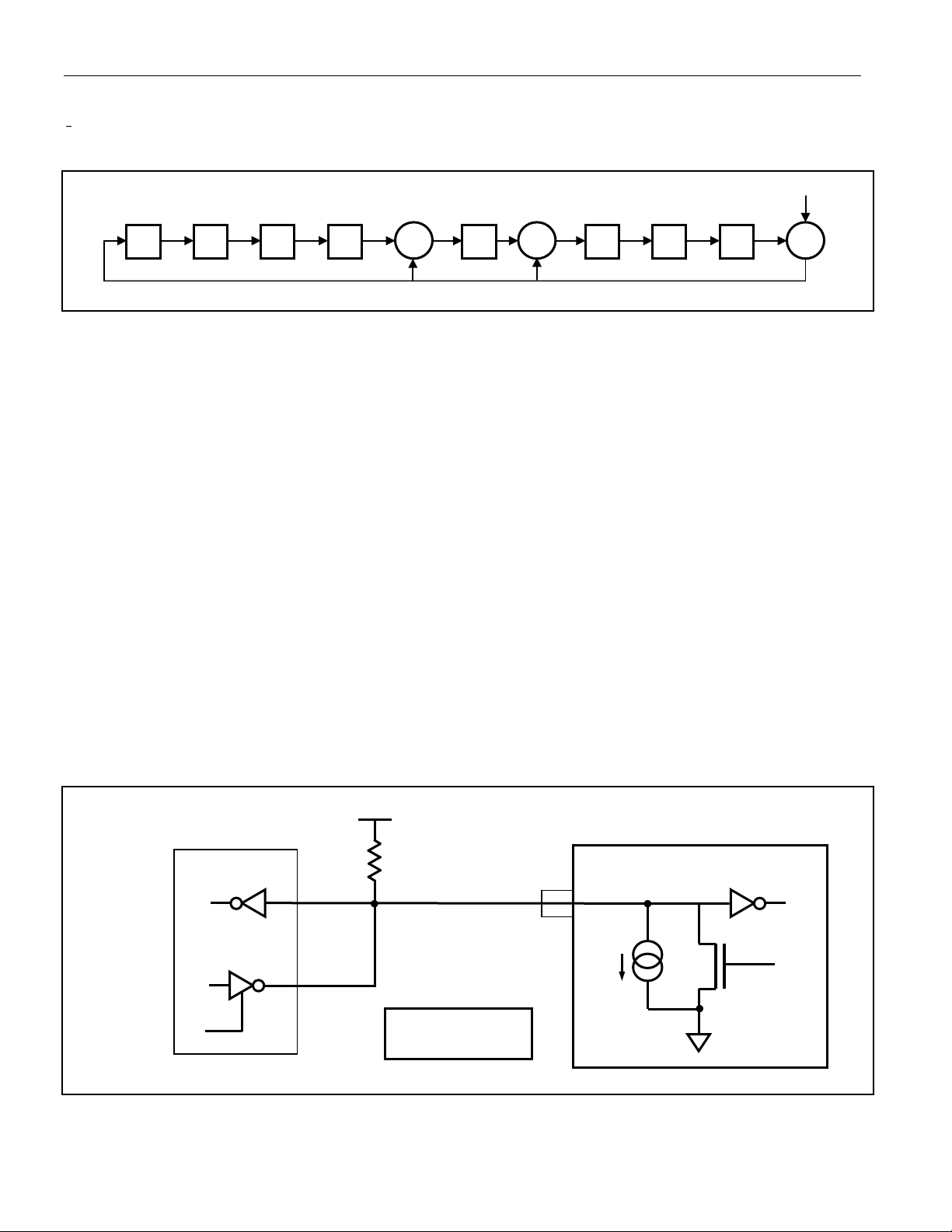
CRC GENERATION
CRC bytes are provided as part of the DS18B20’s 64-bit ROM code a nd in the 9th byte of the scratchpad
memory. The ROM code CRC is calculat ed from the first 56 bits of the ROM code and is contained in the
most significant byte of the ROM. The scratchpad CRC is calculated from the data stored in the
scratchpad, and there fore it changes w hen the data in the scratchpad c hanges. The CRCs pro vide the bu s
master with a method o f data validat ion when da ta is read from the DS18B20. To verify that dat a has
been read cor rectly, the bus master must re-calculat e the CRC from the received d ata and then co mpare
this value to either the ROM code CRC (for ROM reads) o r to the scratchpad C RC (for scratchpad reads).
If the calculated CRC matches the read CRC, t he data has been received err or free. The comparison o f
CRC values and t he dec ision t o co ntinue w ith a n ope ration a re det ermin ed ent irely by the bus ma ster .
There is no circuitry inside the DS18B20 that prevents a command sequence from proceeding if the
DS18B20 CRC (ROM or scratchpad) do es not match the value generated by the bus master.
The e quivalent p olynomial function of the C R C (ROM or scra tchpad) is:
CRC = X8 + X5 + X4 + 1
The bus master can re-ca lculat e t he CRC and co mpare it to the CRC value s fro m the DS18B20 using t he
po lynom ial g ener at or sho wn in Figure 9. This circuit consists o f a shift register and XOR gates, and the
shift register b its are initialized t o 0. Start ing with the least signif icant bit of the ROM code o r the least
significant bit o f byte 0 in t he scrat chpad, one bit at a time should shifted into the shift register. After
shifting in the 56th bit from the ROM or the most significant bit of byte 7 from the scratchpad, the
po lynom ial ge nera tor will co nt ain t he re-calculated CRC. Next, the 8-bit ROM code or scrat chpad CRC
from the DS18B20 must be shifted into the circuit. At this point, if the re-calculated CRC was co r rect, the
shift regis ter will cont ain all 0s. Additional infor mation about the Maxim 1-Wire cyclic redundancy check
8 of 22
Page 9
DS18B20
(MSB)
(LSB)
XOR
XOR
INPUT
VPU
4.7k
5μA
Rx
Tx
DS18B20 1-Wire PORT
100Ω
MOSFET
TX
Rx
Rx = RECEIVE
Tx = TRANSMIT
1-Wire BUS
DQ
is a vailab le in Application Note 27: Understanding and Using Cyclic Redundancy Checks with Maxim
iButton Products.
Figure 9. CRC Generator
XOR
1-WIRE BUS SYSTEM
The 1 -Wire bus s ystem uses a s ingle bus mast er to co ntrol one or more s lave devices. T he DS18B20 is
always a slave. When there is only one slave on the bus, the system is referred to as a “single-drop”
system; the system is “multidrop” if there are multip le sla ves on the bus.
All data and commands are tr ansmitted least significa nt bit first over the 1-Wire bus.
The following discussion of the 1-Wire bus system is broken down into three topics: hardware
configuration, t r ansaction sequence, and 1-Wire signaling (signal types and timing).
HARDWARE CONFIGURATION
The 1-Wire bus has by definition onl y a single data line. Each de vice (master or s lave) interfaces to the
data line via an open-drain or 3-state port. This allows e ach device to “release” the data line w hen t he
dev ice is no t t rans mitt ing d at a so the bus is a vail able for use by a not her de vice. The 1-Wire port of the
DS1 8B20 (the DQ pin) is o pen drain with an inte rnal c ircuit equivalent to that s hown in Figure 10.
The 1-Wire bus requires an external pullup resistor of approximately 5kΩ; thus, the idle state for the
1-Wire bus is high. If for any reason a t r ansaction needs to be suspe nded, the bus MUST be left in the idle
state if the transact ion is to resume. Infin ite recovery time can occur bet ween bits so long as the 1-Wire
bus is in the inact ive (high) st ate dur ing the recover y period. If the bus is held low for more than 480µs,
all c omponents on the bus will be reset .
Figure 10. Hardware Configuration
PIN
TYP
9 of 22
Page 10

DS18B20
TRANSACTION SEQUENCE
The transact ion sequence for access ing the DS18B20 is as fo llows:
Step 1. Initialization
Step 2. ROM Command (followed by any required data exchange)
Step 3. DS18B20 Function Command (followed by any required data exchange)
It is very important to follow this sequence every ti me t he DS18B20 is accessed, as the DS18B20 wi ll no t
respond if a ny steps in the seque nce are missing o r out of order. Except ions t o this rule are the S earch
ROM [F0h] and Alarm Search [ECh] commands. After issuing either of these ROM commands, the
master must retur n to St ep 1 in the sequence.
INITIALIZATION
All transactions on the 1-Wire bus begin with an initialization sequence. The initialization sequence
consists of a reset p ulse transmitt ed by the bus master followed by presence pu lse(s) transmitted by the
slave(s). The prese nce pu lse let s the bus mast er kno w t hat slave devices (such as the DS18B20) are on the
bus and are read y t o op erate. Timing for the reset and presence pu lses is deta iled in the 1-Wire Signaling
section.
ROM COMMANDS
After the bus master has detected a presence pulse, it can issue a ROM command. These commands
operate on the unique 64-bit ROM cod es of each slave device a nd a l low the master to s ingle out a specific
device if many are present on the 1-Wire bus. These commands also a llow the master to determine how
many and what types of devices are present on the bus or if any device has experienced an alarm
co ndition. There are five ROM commands, and each command is 8 bits long. The master device must
issue an appropriate ROM command before issuing a DS18B20 function command. A flowchart for
op eratio n of the ROM commands is show n in Figure 11.
SEARCH ROM [F0h]
When a system is in itially powered u p, the master must identify the ROM co des of all slave de vices on
the bus, which allows the master to determine the number of slaves and their device types. The master
learns the ROM codes through a process of elimination that r eq uires the ma ster to perform a Search ROM
cycle (i.e., S earch ROM co mmand fo llowed by da t a exchange) as many t imes as neces sary to ident ify all
of the slave dev ices. If there is only o ne slave on t he bus, the simp ler Read ROM command (see below)
can be used in place of the Search ROM process. For a detailed explanation of the Search ROM
procedure, refer to the iButton® Book of Standards at www.maxim-ic.com/ibuttonbook. After every
Search ROM cycle, the bus master must retu r n to St ep 1 (Initialization) in the transaction sequence.
READ ROM [33h]
This co mma nd ca n o nly be used w he n t here is o ne s la ve o n t he bu s. I t allo ws the bu s mas te r to read the
sla ve’ s 64 -bit ROM cod e without us ing the Search ROM pro cedure. If th is co mma nd is u se d w hen t her e
is more than one slave present on the bus, a data collision will occur when all the slaves attempt to
respond at the same time.
MATCH ROM [55h]
The match ROM command fo llowed by a 64-bit ROM code sequence a llows the bus master to address a
spec ific sla ve dev ice on a multidr op or s ingle-dro p bus. Only the slave t hat exactly matches the 64-bit
ROM code sequence will respo nd to the function command issu ed b y the mast er ; all ot her slave s on t he
bus will wait for a reset pulse.
iButton is a registered trademark of Maxim Integrat ed Products, Inc .
10 of 22
 Loading...