

Page 1
r
y
www.maxim-ic.com
FEATURES
§ Two linear taper potentiometers
- DS1855-010 (one 10k, 100 position and
one 10k, 256 position)
- DS1855-020 (one 10k, 100 position and
one 20k, 256 position)
- DS1855-050 (one 10k, 100 position and
one 50k, 256 position)
- DS1855-100 (one 10k, 100 position and
one 100k, 256 position)
§ 256 bytes of EEPROM memory
§ Access to data and potentiometer control via
Dual Nonvolatile Digital Potentiomete
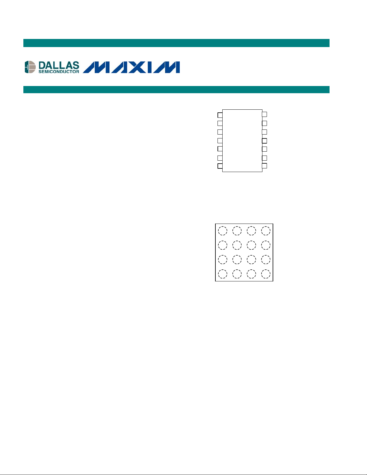
SDA 1 14 Vcc
SCL 2
A0
GND
3
A1 4 11 H1
A2 5
WP 6 9 W0
78
14-Pin TSSOP (173-mil)
13
12
10
DS1855
and Secure Memor
H0
W1
L1
L0
a 2-wire interface
§ External write-protect pin to protect data and
Top View
potentiometer settings
§ Data and potentiometer settings also can be
write-protected through software control
§ Nonvolatile wiper storage
§ Operates from 3V or 5V supplies
§ Packaging: 14-pin TSSOP, 16-ball CSBGA,
flip-chip package
A
B
C
D
§ Industrial operating temperature:
-40ºC to +85ºC
14-Pin Flip Chip (100-mil x 100-mil)
1 2 3 4
16-Ball CSBGA (4mm x 4mm)
(Not Shown)
DESCRIPTION
The DS1855 dual nonvolatile (NV) digital potentiometer and secure memory consists of one 100-position
linear taper potentiometer, one 256-position linear taper potentiometer, 256 bytes of EEPROM memory,
and a 2-wire interface. The DS1855, which features a new software write protect, is an upgrade of the
DS1845. The DS1855 provides an ideal method for setting bias voltages and currents in control
applications using a minimum of circuitry. The EEPROM memory allows a user to store configuration or
calibration data for a specific system or device as well as provide control of the potentiometer wiper
settings. Any type of user information may reside in the first 248 bytes of this memory. The next two
addresses of EEPROM memory are for potentiometer settings and the remaining 6 bytes of memory are
reserved. These reserved and potentiometer registers should not be used for data storage. Access to this
EEPROM is via an industry-standard 2-wire bus. The interface I/O pins consist of SDA and SCL. The
wiper position of the DS1855, as well as EEPROM data, can be write-protected through hardware using
the write-protect input pin (WP) or software using the 2-wire interface.
1 of 1 032205
Page 2

PIN DESCRIPTIONS
Name TSSOP BGA Description
VCC 14 A3 Power Supply Terminal. The DS1855 will support supply
voltages ranging from +2.7V to +5.5V.
GND 7 D1 Ground Terminal.
SDA 1 B2 2-Wire serial data interface. The serial data pin is for serial data
transfer to and from the DS1855. The pin is open drain and may
be wire-ORed with other open drain or open collector interfaces.
SCL 2 A2 2-Wire Serial Clock Input. The serial clock input is used to
clock data into the DS1855 on rising edges and clock data out on
falling edges.
WP 6 C1 Write Protect Input. If set to logic 0, the data in memory and the
potentiometer wiper setting may be changed. If set to logic 1, both
the memory and the potentiometer wiper settings will be write
protected. The WP pin is pulled high internally.
A0 3 A1 Address Input. Pins A0, A1, and A2 are used to specify the
address of each DS1855 when used in a multi-dropped
configuration. Up to eight DS1855s may be addressed on a single
2-wire bus.
A1 4 B1 Address Input.
A2 5 C2 Address Input.
H0 13 A4 High terminal of Potentiometer 0. For both potentiometers, it is
not required that the high terminal be connected to a potential
greater than the low terminal. Voltage applied to the high terminal
of each potentiometer cannot exceed VCC or go below ground.
H1 11 B3 High terminal of Potentiometer 1.
L0 8 D3 Low terminal of Potentiometer 0. For both potentiometers, it is
not required that the low terminal be connected to a potential less
than the high terminal. Voltage applied to the low terminal of each
potentiometer cannot exceed VCC or go below ground.
L1 10 C4 Low terminal of Potentiometer 1.
W0 9 D4 Wiper terminal of Pot 0. The wiper position of Potentiometer 0
is determined by the byte at EEPROM memory location F9h.
Voltage applied to the wiper terminal of each potentiometer cannot
exceed the power supply voltage, V
W1 12 B4 Wiper terminal of Pot 1. The wiper position of Potentiometer 1
is determined by the byte at EEPROM memory location F8h.
NC C3 No Connect.
NC D2 No Connect.
, or go below ground.
CC
DS1855
2 of 2
Page 3
DS1855
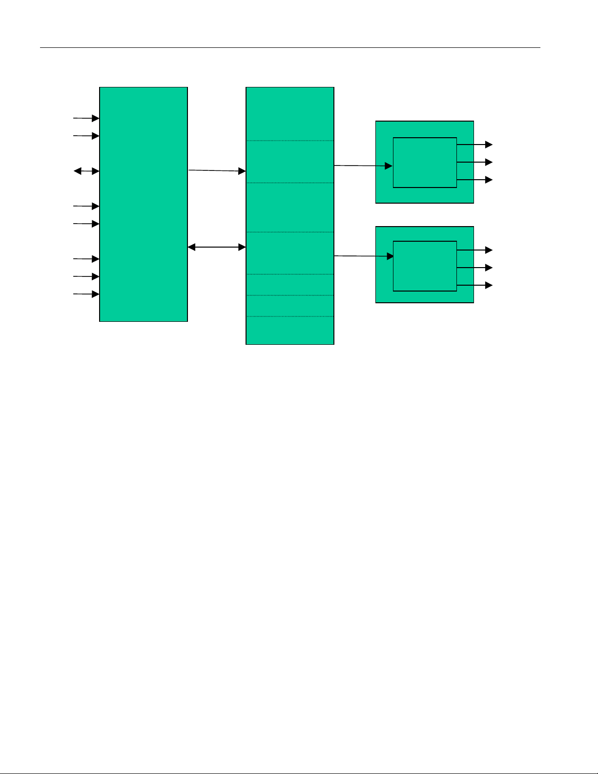
DS1855 BLOCK DIAGRAM Figure 1
V
CC
GND
SDA
SCL
WP
A0
A1
A2
2-WIRE
INTERFACE
CONTROL
DATA
Up to eight DS1855s can be installed on a single 2-wire bus. Access to an individual device is achieved
by using a device address that is determined by the logic levels of address pins A0 through A2.
Additionally, the DS1855 will operate from 3V or 5V supplies. Three package options are available: 14pin TSSOP, 16-ball CSBGA, and flip-chip package.
248 BYTES
EEPROM
MEMORY
1 BYTE WIPER
SETTING
POT 0
1 BYTE WIPER
SETTING
POT 1
CONFIGURATION
BYTE
LOCK BYTE
LOCK BYTE
RESERVED
POTENTIOMETER 0
100-
Position
Pot
POTENTIOMETER 1
256-
Position
Pot
H0
W0
L0
H1
W1
L1
3 of 3
Page 4

DS1855
MEMORY ORGANIZATION
The DS1855’s serial EEPROM is internally organized with 256 words of 1 byte each. Each word requires
an 8-bit address for random word addressing. The byte at address F9h determines the wiper setting for
potentiometer 0, which contains 100 positions. Writing values above 63h to this address sets the wiper to
its uppermost position, but the MSB is ignored. The byte at address F8h determines the wiper setting for
potentiometer 1, which contains 256 positions (00h to FFh). Address locations FAh though FFh are
reserved and should not be written.
MEMORY
LOCATION
00h – F7h User Memory General-purpose user memory.
F8h Potentiometer 1 Setting Writing to this byte controls the setting of potentiometer 1, a 256-
F9h Potentiometer 0 Setting Writing to this byte controls the setting of potentiometer 0, a 100-
FAh Software Lock
NAME OF
MEMORY
LOCATION
Configuration Byte
FUNCTION OF MEMORY LOCATION
position pot. Valid settings are 00h to FFh.
position pot. Valid settings are 00h to 63h. MSB is ignored.
The three lower bits in this byte can be used to set write-protection
to the 256-byte memory block.
B2 B1 B0
B2: Writing this bit to a 1 protects the upper page of memory. If
this bit is set, memory locations F8h to FFh are configured for
write-protection.
B1: Writing this bit to a 1 protects the upper block of memory. If
this bit is set, memory locations 80h to F7h are configured for
write-protection. The upper page must be unlocked in order to
modify the locking of this portion of memory.
B0: Writing this bit to a 1 protects the lower block of memory. If
this bit is set, memory locations 00h to 7Fh are configured for
write-protection. The upper page must be unlocked in order to
modify the locking of this portion of memory.
4 of 4
Page 5

DS1855
FBh – FCh Lock Bytes Writing to these two bytes allows the user to lock or unlock the
memory described in byte FAh.
LOCK: If memory location FBh is written to 56h and memory
location FCh is written to 25h, the device will enter lock mode.
Write protection will become active in the memory locations that
are specified in FAh.
UNLOCK: If memory location FBh is written to 67h and memory
location FCh is written to 36h, the device will be unlocked. Once
unlocked, the user can change the setting of memory location FAh
to affect the EEPROM write-protection.
The locking can be updated at any time as long as the upper
page is unlocked.
FD – FFh Reserved Reserved
5 of 5
Page 6

DS1855
2-WIRE OPERATION
Clock and Data Transitions
The SDA pin is normally pulled high with an external resistor or device. Data on the SDA pin may only
change during SCL low time periods. Data changes during SCL high periods will indicate a START or
STOP conditions depending on the conditions discussed below. Refer to the timing diagram in Figure 2
for further details.
START Condition
A high-to-low transition of SDA with SCL high is a START condition that must precede any other
command. Refer to the timing diagram in Figure 2 for further details.
STOP Condition
A low-to-high transition of SDA with SCL high is a STOP condition. After a read sequence, the stop
command places the DS1855 into a low-power mode. Refer to the timing diagram in Figure 2 for further
details.
Acknowledge
All address and data bytes are transmitted via a serial protocol. The DS1855 pulls the SDA line low
during the ninth clock pulse to acknowledge that it has received each word.
Standby Mode
The DS1855 features a low-power mode that is automatically enabled after power-on, after a STOP
command, and after the completion of all internal operations.
2-Wire Interface Reset
After any interruption in protocol, power loss, or system reset, the following steps reset the DS1855:
1. Clock up to nine cycles.
2. Look for SDA high in each cycle while SCL is high.
3. Create a START condition while SDA is high.
Device Addressing
The DS1855 must receive an 8-bit device address word following a START condition to enable a specific
device for a read or write operation. The address word is clocked into the DS1855 MSB to LSB. The
address word consists of Ah (1010) followed by A2, A1, and A0 then the read/write (R/W) bit. If the
R/W bit is high, a read operation is initiated. If the R/W is low, a write operation is initiated. For a device
to become active, the values of A2, A1, and A0 must be the same as the hard-wired address pins on the
DS1855. Upon a match of written and hard-wired addresses, the DS1855 will output a zero for one clock
cycle as an acknowledge. If the address does not match, the DS1855 returns to a low-power mode.
Write Operations
After receiving a matching address byte with the R/W bit set low, the device goes into the write mode of
operation. The master must transmit an 8-bit EEPROM memory address to the device to define the
address where the data is to be written. After the reception of this byte, the DS1855 will transmit a zero
for one clock cycle to acknowledge the receipt of the address. The master must then transmit an 8-bit data
word to be written into this address. The DS1855 will again transmit a zero for one clock cycle to
acknowledge the receipt of the data. At this point, the master must terminate the write operation with a
STOP condition. The DS1855 then enters an internally timed write process T
All inputs are disabled during this byte write cycle.
6 of 6
to the EEPROM memory.
w
Page 7

DS1855
The DS1855 is capable of an 8-byte page write. A page write is initiated the same way as a byte write, but
the master does not send a STOP condition after the first byte. Instead, after the slave acknowledges
receipt of the data byte, the master can send up to seven more bytes using the same nine-clock sequence.
The master must terminate the write cycle with a STOP condition or the data clocked into the DS1855
will not be latched into permanent memory.
Acknowledge Polling
Once the internally timed write has started and the DS1855 inputs are disabled, acknowledge polling can
be initiated. The process involves transmitting a START condition followed by the device address. The
R/W bit signifies the type of operation that is desired. The read or write sequence will only be allowed to
proceed if the internal write cycle has completed and the DS1855 responds with a zero.
Read Operations
After receiving a matching address byte with the R/W bit set high, the device goes into the read mode of
operation. There are three read operations: current address read, random read, and sequential address
read.
CURRENT ADDRESS READ
The DS1855 has an internal address register that maintains the address used during the last read or write
operation, incremented by one. This data is maintained as long as VCC is valid. If the most recent address
was the last byte in memory, the register resets to the first address. This address stays valid between
operations as long as power is available.
Once the device address is clocked in and acknowledged by the DS1855 with the R/W bit set to high, the
current address data word is clocked out. The master does not respond with a zero, but does generate a
STOP condition afterwards.
RANDOM READ
A random read requires a dummy-byte write sequence to load in the data word address. Once the device
and data address bytes are clocked in by the master and acknowledged by the DS1855, the master must
generate another START condition. The master now initiates a current address read by sending the device
address with the read/write bit set high. The DS1855 acknowledges the device address and serially clocks
out the data byte.
SEQUENTIAL ADDRESS READ
Sequential reads are initiated by either a current address read or a random address read. After the master
receives the first data byte, the master responds with an acknowledge. As long as the DS1855 receives
this acknowledge after a byte is read, the master may clock out additional data words from the DS1855.
After reaching address FFh, it resets to address 00h.
The sequential read operation is terminated when the master initiates a STOP condition. The master does
not respond with a zero.
For a more detailed description of 2-wire theory of operation, refer to the next section.
7 of 7
Page 8

DS1855
2-WIRE SERIAL PORT OPERATION
The 2-wire serial port interface supports a bidirectional data transmission protocol with device
addressing. A device that sends data on the bus is defined as a transmitter, and a device receiving data is
defined as a receiver. The device that controls the message is called a “master.” The devices that are
controlled by the master are “slaves.” The bus must be controlled by a master device that generates the
serial clock (SCL), controls the bus access, and generates the START and STOP conditions. The DS1855
operates as a slave on the two-wire bus. Connections to the bus are made via the open-drain I/O lines,
SDA and SCL. The following I/O terminals control the 2-wire serial port: SDA, SCL, A0, A1, A2.
Timing diagrams for the 2-wire serial port can be found in Figures 2 and 3. Timing information for the 2wire serial port is provided in the AC Electrical Characteristics Table for 2-wire serial communications.
The following bus protocol has been defined:
1. Data transfer may be initiated only when the bus is not busy.
2. During data transfer, the data line must remain stable whenever the clock line is HIGH. Changes in
the data line while the clock line is HIGH will be interpreted as control signals.
Accordingly, the following bus conditions have been defined:
Bus not busy: Both data and clock lines remain HIGH.
Start data transfer: A change in the state of the data line from HIGH to LOW while the clock is HIGH
defines a START condition.
Stop data transfer: A change in the state of the data line from LOW to HIGH while the clock line is
HIGH defines the STOP condition.
Data valid: The state of the data line represents valid data when, after a START condition, the data line
is stable for the duration of the clock signal’s HIGH period. The data on the line can be changed during
the clock signal’s LOW period. There is one clock pulse per bit of data. Figures 2 and 3 detail how data
transfer is accomplished on the 2-wire bus. Depending on the state of the R/W bit, two types of data
transfer are possible.
Each data transfer is initiated with a START condition and terminated with a STOP condition. The
number of data bytes transferred between START and STOP conditions is not limited and is determined
by the master device. The information is transferred byte-wise and each receiver acknowledges with a 9
bit.
A regular mode (100kHz clock rate) and a fast mode (400kHz clock rate) are defined within the bus
specifications. The DS1855 works in both modes.
Acknowledge: Each receiving device, when addressed, is obliged to generate an acknowledge after the
reception of each byte. The master device must generate an extra clock pulse, which is associated with
this acknowledge bit.
A device that acknowledges must pull down the SDA line during the acknowledge clock pulse in such a
way that the SDA line is a stable LOW during the HIGH period of the acknowledge-related clock pulse.
Of course, setup and hold times must be taken into account. A master must signal an end of data to the
slave by not generating an acknowledge bit on the last byte that has been clocked out of the slave. In this
case, the slave must leave the data line HIGH to enable the master to generate the STOP condition.
8 of 8
th
Page 9

DS1855
1. Data transfer from a master transmitter to a slave receiver. The first byte transmitted by the master is
the command/control byte. Next, follows a number of data bytes. The slave returns an acknowledge
bit after each received byte.
2. Data transfer from a slave transmitter to a master receiver. The master transmits the first byte (the
command/control byte) to the slave. The slave then returns an acknowledge bit. Next, follows a
number of data bytes transmitted by the slave to the master. The master returns an acknowledge bit
after all received bytes other than the last byte. At the end of the last received byte, a ‘not
acknowledge’ can be returned.
The master device generates all serial clock pulses and the START and STOP conditions. A transfer is
ended with a STOP condition or with a repeated START condition. Since a repeated START condition is
also the beginning of the next serial transfer, the bus will not be released.
The DS1855 may operate in the following two modes:
1. Slave receiver mode: Serial data and clock are received through SDA and SCL, respectively. After
each byte is received, an acknowledge bit is transmitted. START and STOP conditions are recognized
as the beginning and end of a serial transfer. Address recognition is performed by hardware after
reception of the slave (device) address and direction bit.
2. Slave transmitter mode: The first byte is received and handled as in the slave receiver mode.
However, in this mode the direction bit will indicate that the transfer direction is reversed. Serial data
is transmitted on SDA by the DS1855 while the serial clock is input on SCL. START and STOP
conditions are recognized as the beginning and end of a serial transfer.
3. Slave Address: Command/control byte is the first byte received following the START condition from
the master device. The command/control byte consists of a 4-bit control code. For the DS1855, this is
set as 1010 binary for read/write operations. The next 3 bits of the command/control byte are the
device select bits or slave address (A2, A1, A0). They are used by the master device to select which
of eight devices is to be accessed. When reading or writing to the DS1855, the device-select bits must
match the device-select pins (A2, A1, A0). The last bit of the command/control byte (R/W) defines
the operation to be performed. When set to a 1 a read operation is selected, and when set to a 0 a write
operation is selected.
Following the START condition, the DS1855 monitors the SDA bus by checking the device type
identifier being transmitted. Upon receiving the 1010 control code, the appropriate device address bits,
and the R/W bit, the slave device outputs an acknowledge signal on the SDA line.
WRITE PROTECT
An external write-protect (WP) pin protects EEPROM data and potentiometer position from alteration in
an application. If this pin is open or tied high, the EEPROM content, which includes the potentiometer
settings, is protected from alteration. If no activity occurs on the SDA and SCL pins, this part will be held
in a low-power mode. The EEPROM and potentiometer settings may be read if WP is set, but they cannot
be written under any circumstances unless WP is taken to GND.
9 of 9
Page 10

DS1855
LOCKING AND UNLOCKING EEPROM
In addition to the WP pin, it is possible to write-protect, or lock, certain portions of the EEPROM through
software control. The DS1855 256-byte EEPROM can be visualized as three blocks, or partitions. The
lower block is from 00h to 7Fh. The upper block is 80h to F7h. And the upper page is from F8 to FFh.
The lower and upper blocks are user EEPROM. The upper page is EEPROM that contains the pot
settings, as well as the lock registers.
Locking the EEPROM is a two-step process. First, the software lock configuration byte (FAh) is used to
choose which portion(s) of EEPROM are to be locked. The three least significant bits of FAh are B2, B1,
and B0. B2 selects the upper page (F8–FFh). B1 selects the upper block (80–F7h). The LSBit, B0, selects
the lower block (00–7Fh). The user may lock one, two, or all three partitions at once. The second step
required to turn on the lock is to write the password into the lock bytes (FBh and FCh). The password to
lock is 56h, 25h (FBh and FCh, respectively). Once the EEPROM is locked, the user may still read data
out of the locked portions, but performing a write will not write to EEPROM.
Unlocking the EEPROM consists of entering the password into bytes FBh and FCh. The password to
unlock is 67h, 36h (FBh and FCh, respectively). However, when attempting to unlock the upper page,
which contains the lock bytes (FBh and FCh), the two-byte password must be written in one write cycle.
If a 2-wire STOP command is sent between the write to FBh and FCh, the upper page will remain locked.
In order to modify the Software Lock Configuration Byte (FAh), the upper page must be unlocked. In
other words, the upper page must be unlocked in order to make changes to the locking of the upper and
lower blocks.
READING AND WRITING THE POTENTIOMETER VALUES
Reading from and writing to the potentiometers consists of a standard read or write to EEPROM memory
at the addresses F8h and F9h. The 8-bit value at address F9h controls the wiper setting for potentiometer
0, which has 100 positions. The 8-bit value at address F8h controls the wiper setting of potentiometer 1,
which has 256 positions. Potentiometer 1 may be set to any value between 00h and FFh. 00h sets the
wiper of potentiometer 1 to its lowest value and FFh sets the wiper to its highest. Potentiometer 0 may be
set to any value between 00h and 63h. A value of 00h sets the wiper of potentiometer 0 to its lowest
position and 63h sets the wiper to its highest position. Any hexadecimal value is a valid address. Setting a
value greater than the upper limit of the potentiometer’s range, 64h or greater for potentiometer 0, will
result in setting the wiper to its highest position, but the MSB will be ignored. The memory locations F8h
and F9h, which control the potentiometers’ settings, are programmed to FFh when shipped from the
factory. All other memory locations are initially programmed to 00h.
10 of 10
Page 11
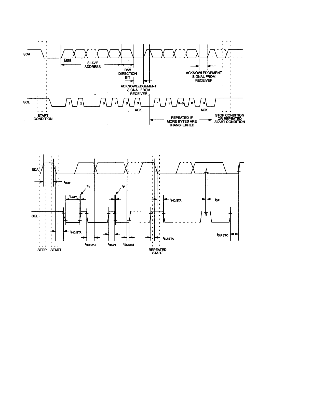
2-WIRE PROTOCOL DATA TRANSFER PROTOCOL Figure 2
2-WIRE AC CHARACTERISTICS Figure 3
DS1855
11 of 11
Page 12

DS1855
ABSOLUTE MAXIMUM RATINGS*
Voltage on Any Pin Relative to Ground -0.3V to +6.0V
Operating Temperature Range -40°C to +85°C; Extended Industrial
Programming Temperature Range 0°C to +85°C
Storage Temperature Range -55°C to +125°C
Soldering Temperature See J-STD-020A Specification
* This is a stress rating only and functional operation of the device at these or any other conditions above
those indicated in the operation sections of this specification is not implied. Exposure to absolute
maximum rating conditions for extended periods of time may affect reliability.
The Dallas Semiconductor DS1855 is built to the highest quality standards and manufactured for longterm reliability. All DS1855s are made using the same quality materials and manufacturing methods.
However, the DS1855 in the flip-chip package is not exposed to environmental stresses, such as burn-in,
that some industrial applications require. For specific reliability information on this product, please
contact the factory in Dallas at (972) 371-4448.
RECOMMENDED DC OPERATING CONDITIONS (-40°C to +85°C)
PARAMETER SYMBOL MIN TYP MAX UNITS NOTES
Supply Voltage VCC +2.7 5.5 V 1
DC ELECTRICAL CHARACTERISTICS (-40°C to +85°C; VCC = 2.7V to 5.5V)
PARAMETER SYMBOL CONDITION MIN TYP MAX UNITS NOTES
Active Supply Current
Input Leakage ILI -1 +1 mA
Input Logic 1 VIH 0.7VCC V
Input Logic 0 VIL GND -
Input Current each
I/O Pin
Standby Current
Voltage (SDA)
ICC 0.5 mA 11, 12
CC
+
V
0.3
0.3VCC V
0.3
0.4<V
I/O
-10 +10 mA 3
<0.9VDD
3.0V
I
stby
5.0V
V
3mA sink
OL1
20
30
0.0 0.4 V Low-Level Output
40
60
mA 2
current
6mA sink
V
OL2
0.0 0.6 V
current
I/O Capacitance C
WP Internal Pull-Up
Resistance, R
wp
10 pF
I/O
40 65 100
R
wp
12 of 12
kW
Page 13

DS1855
ANALOG RESISTOR CHARACTERISTICS (-40°C to +85°C; V
= 2.7V to 5.5V)
CC
PARAMETER SYMBOL CONDITION MIN TYP MAX UNITS NOTES
Resistor Inputs L, H, W GND -
VCC+0.3 V
0.3
Wiper Resistance
RW 3.0V
5.0V
400
250
1000
600
W
Wiper Current IW 2 mA
End-to-End Resistance
Absolute Linearity
Relative Linearity
-3dB Cutoff
+25°C -20 +20 %
10kW/100 pos.
10kW/256 pos.
20kW/256 pos.
50kW/256 pos.
100kW/256 pos.
10kW/100 pos.
all other pots
f
DS1855-010 1 MHz
cutoff
-0.75
-0.75
-1.0
-1.5
-2.25
-0.25
-0.5
0.75
0.75
1.0
1.5
2.25
+0.25
0.5
LSB 9
LSB 10
Frequency
End-to-End Temp.
Coefficient
750
ppm/°C
13 of 13
Page 14

DS1855
AC ELECTRICAL CHARACTERISTICS (-40°C to +85°C, V
= 2.7V to 5.5V)
CC
PARAMETER SYMBOL CONDITION MIN TYP MAX UNITS NOTES
SCL Clock Frequency f
Bus Free Time Between
STOP and START
Hold Time (repeated)
START Condition
Low Period of SCL
Clock
High Period of SCL
Clock
Data Hold Time t
Data Set-Up Time t
Start Set-Up Time t
Rise Time of Both SDA
and SCL Signals
Fall Time of Both SDA
and SCL Signals
Set-Up Time for STOP
Condition
Capacitive Load for
Fast Mode
SCL
Standard Mode
t
Fast Mode
BUF
Standard Mode
t
Fast Mode
HD:STA
Standard Mode
t
Fast Mode
LOW
Standard Mode
t
Fast Mode
HIGH
Standard Mode
HD:DAT
Fast Mode
Standard Mode
Fast Mode
SU:DAT
Standard Mode
Fast Mode
SU:STA
Standard Mode
tR Fast Mode
Standard Mode
tF Fast Mode
Standard Mode
t
Fast Mode
SU:STO
Standard Mode
0
0
1.3
4.7
0.6
4.0
1.3
4.7
0.6
4.0
0
0
100
250
0.6
4.7
20+0.1CB
20+0.1CB
0.6
4.0
400
100
kHz 4
ms
4
ms
4,5
ms
4
ms
4
0.9
0.9
ms
4,6
ns 4
ms
4
300
1000
300
300
ns 4
ns 7
ms
CB 400 pF 7
Each Bus Line
EEPROM Write Time TW 2.5 10 ms 8
NONVOLATILE MEMORY CHARACTERISTICS
PARAMETER SYMBOL CONDITION MIN TYP MAX UNITS
Writes +85°C 50,000
14 of 14
Page 15

DS1855
NOTES:
1. All voltages are referenced to ground.
2. I
3. I/O pins of fast-mode devices must not obstruct the SDA and SCL lines if VCC is switched off.
4. A fast mode-device can be used in a standard mode system, but the requirement t
5. After this period, the first clock pulse is generated.
6. The maximum t
7. C
8. EEPROM write begins after a STOP condition occurs.
9. Absolute linearity is used to measure expected wiper voltage as determined by wiper position.
10. Relative linearity is used to determine the change of wiper voltage between two adjacent wiper
11. ICC specified with SDA pin open.
12. Maximum ICC is dependent on clock rates.
specified with for V
STBY
= 3.0V and 5.0V, and control port logic pins are driven to the appropriate
CC
logic levels. Appropriate logic levels specify that logic inputs are within a 0.5V of ground or VCC for
the corresponding inactive state.
> 250ns must
SU:DAT
then be met. This will automatically be the case if the device does not stretch the LOW period of the
SCL signal. If such a device does stretch the LOW period of the SCL signal, it must output the next
data bit to the SDA line t
has only to be met if the device does not stretch the LOW period (t
HD:DAT
RMAX
+ t
SU:DAT
= 1000 + 250 = 1250ns before the SCL line is released.
LOW
) of the
SCL signal.
– Total capacitance of one bus line in picofarads, timing referenced to (0.9)(VCC) and (0.1)(VCC).
B
positions.
15 of 15
Page 16
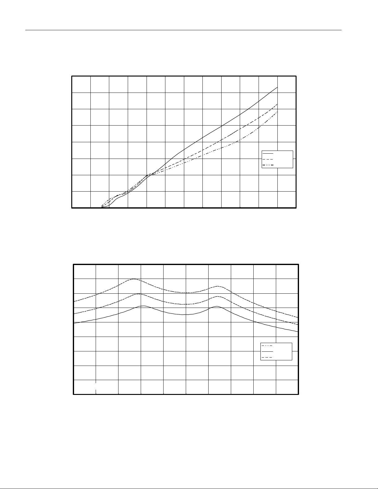
TYPICAL OPERATING CHARACTERISTICS
(
)
(
m
)
= 5V, T = +25ºC, unless otherwise specified)
(V
CC
SUPPLY CURRENT vs. VOLTAGE
40
35
A
30
25
20
DS1855
15
10
5
0
0123456
Icc @-40C
Icc @25C
Icc @85
VOLTAGE (V)
WIPER RESISTANCE vs. WIPER VOLTAGE
450
400
SUPPLY CURRENT
350
W
300
250
200
150
100
WIPER RESISTANCE
50
POT 0, TAP 99
0
0 0.5 1 1.5 2 2.5 3 3.5 4 4.5 5
VOLTAGE (V)
25 Deg. C
-40 Deg C
85 Deg C
16 of 16
Page 17
TYPICAL OPERATING CHARACTERISTICS (cont.)
= 5V, T = +25ºC, unless otherwise specified)
(V
CC
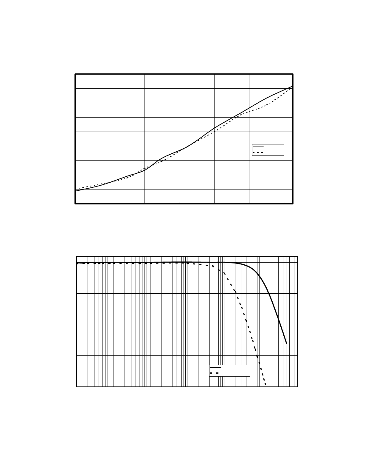
END-TO-END RES % CHANGE vs. TEMPERATURE
2.5%
2.0%
1.5%
1.0%
0.5%
DS1855
0.0%
-0.5%
-1.0%
-1.5%
-2.0%
-40 -20 0 20 40 60 80
END-TO-END RESISTANCE CHANGE (%)
Pot 0 (10K)
Pot 1 (50K)
TEMPERATURE (C)
ATTENUATION vs. FREQUENCY
0
-5
-10
-15
ATTENUATION (dB)
-20
10 100 1,000 10,000 100,000 1,000,000 10,000,000
FREQUENCY (Hz)
17 of 17
Pot 0, 10KOhms
Pot 1, 50kOhms
Page 18
TYPICAL OPERATING CHARACTERISTICS (cont.)
(
m
)
(
)
= 5V, T = +25ºC, unless otherwise specified)
(V
CC
ACTIVE SUPPLY CURRENT vs. FREQUENCY
150
130
110
A
DS1855
90
70
50
SUPPLY CURRENT
30
10
0 50 100 150 200 250 300 350 400
FREQUENCY (kHz)
RESISTANCE vs. VOLTAGE (POWER-UP)
160,000
140,000
W
120,000
100,000
Pot 0 res (50dec)
Pot 1 res (127dec)
Pot 0 res (0dec)
Pot 1 res (0dec)
Pot 0 res (99dec)
Pot 1 res (255dec)
Icc active (uA)
80,000
60,000
40,000
20,000
RESISTANCE FROM W TO L
0
0.0 0.5 1.0 1.5 2.0 2.5 3.0 3.5 4.0 4.5 5.0
Potentiometer value recalled from EEPROM
Pot 1, 0d
Pot 0, 0d
Pot 0, 50d
Pot 1, 255d
Pot 1, 127d
Pot 0, 99d
SUPPLY VOLTAGE - POWER-UP (V)
18 of 18
Page 19

TYPICAL OPERATING CHARACTERISTICS (cont.)
(
)
= 5V, T = +25ºC, unless otherwise specified)
(V
CC
RESISTANCE vs. VOLTAGE (POWER-DOWN)
70,000
60,000
W
50,000
40,000
30,000
Pot 1 set to 255 decimal
Pot 1 set to 127 decimal
DS1855
Pot 0 (50dec)
Pot 1 (127dec )
Pot 0 (0dec)
Pot 1 (0dec)
Pot 0 (99dec)
Pot 1 (255dec )
20,000
Pot 0 set to 99 decimal
10,000
RESISTANCE FROM W TO L
Pot 0 set to 50 decimal
Pot 0 set to 0 decimal
0
Pot 1 set to 0 decimal
0.00.51.01.52.02.53.03.54.04.55.0
SUPPLY VOLTAGE - POWER-DOWN (V)
19 of 19
Page 20

ORDERING INFORMATION
ORDERING
NUMBER
PACKAGE
OPERATING
TEMPERATURE
DS1855E-010 14-PIN TSSOP (173-MIL) -40ºC TO +85ºC
DS1855E-010/T&R 14-PIN TSSOP/TAPE & REEL -40ºC TO +85ºC
DS1855X-010 14-PIN FLIP CHIP -40ºC TO +85ºC
DS1855B-010 16-BALL CSBGA (4X4 MM) -40ºC TO +85ºC
DS1855E-020 14-PIN TSSOP (173-MIL) -40ºC TO +85ºC
DS1855E-020/T&R 14-PIN TSSOP/TAPE & REEL -40ºC TO +85ºC
DS1855X-020 14-PIN FLIP CHIP -40ºC TO +85ºC
DS1855B-020 16-BALL CSBGA (4X4 MM) -40ºC TO +85ºC
DS1855E-050 14-PIN TSSOP (173-MIL) -40ºC TO +85ºC
DS1855E-050/T&R 14-PIN TSSOP/TAPE & REEL -40ºC TO +85ºC
DS1855X-050/T&R 14-PIN FLIP CHIP/TAPE & REEL -40ºC TO +85ºC
DS1855B-050 16-BALL CSBGA (4X4 MM) -40ºC TO +85ºC
DS1855E-100 14-PIN TSSOP (173-MIL) -40ºC TO +85ºC
DS1855E-100/T&R 14-PIN TSSOP/TAPE & REEL -40ºC TO +85ºC
DS1855X-100 14-PIN FLIP CHIP -40ºC TO +85ºC
DS1855B-100 16-BALL CSBGA (4X4 MM) -40ºC TO +85ºC
DS1855B-010+ 16-BALL CSBGA LEAD FREE
DS1855B-010+T&R
16-BALL CSBGA LEAD FREE
TAPE & REEL
DS1855B-010/T&R 16-BALL CSBGA TAPE & REEL
DS1855B-050+ 16-BALL CSBGA LEAD FREE
DS1855E-010+ 16-BALL CSBGA LEAD FREE
DS1855E-010+T&R
16-BALL CSBGA LEAD FREE
TAPE & REEL
DS1855E-050+ 16-BALL CSBGA LEAD FREE
DS1855E-050+T&R
16-BALL CSBGA LEAD FREE
TAPE & REEL
-40°C TO +85°C 10kW/10kW
-40°C TO +85°C
-40°C TO +85°C 10kW/10kW
-40°C TO +85°C 10kW/50kW
-40°C TO +85°C 10kW/10kW
-40°C TO +85°C
-40°C TO +85°C 10kW/50kW
-40°C TO +85°C
DS1855
VERSION
Pot 0/Pot 1
10kW/10kW
10kW/10kW
10kW/10kW
10kW/10kW
10kW/20kW
10kW/20kW
10kW/20kW
10kW/20kW
10kW/50kW
10kW/50kW
10kW/50kW
10kW/50kW
10kW/100kW
10kW/100kW
10kW/100kW
10kW/100kW
10kW/10kW
10kW/10kW
10kW/50kW
20 of 20
 Loading...