

Page 1
r
A
DS1847
Dual Temperature-Controlled
NV Variable Resisto
www.maxim-ic.com
FEATURES
§ Two linear taper, temperature-controlled
variable resistors
§ DS1847-050
- One 50kW, 256 position
- One 10kW, 256 position
§ DS1847-010
- Two 10kW, 256 position
§ Resistor settings changeable every 2°C
§ Access to temperature data and device
control via a 2-wire interface
§ Operates from 3V or 5V supplies
§ Packaging: 14-pin TSSOP, 16-ball CSBGA
§ Operating temperature: -40ºC to +95ºC
§ Programming temperature: 0ºC to +70ºC
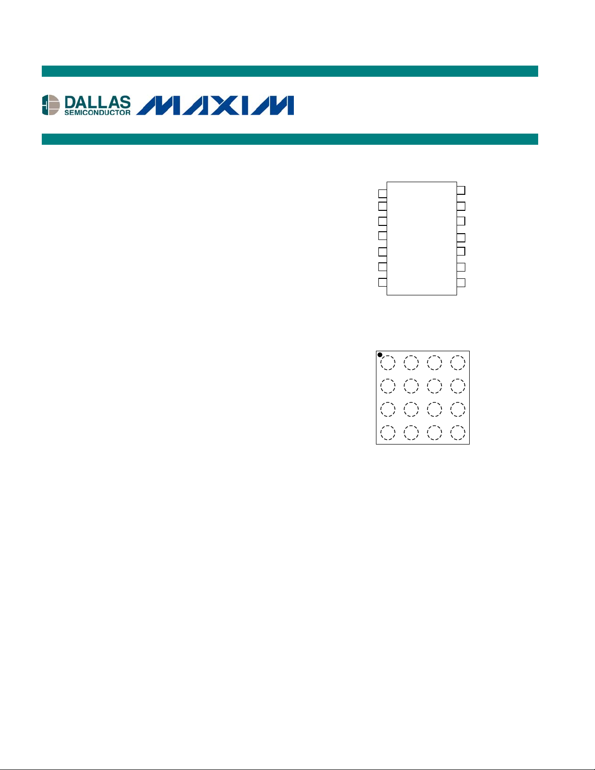
PIN ASSIGNMENT
SDA 1 14 Vcc
SCL 2 13 H0
A0 3 12 NC
A1 4 11 H1
A2 5 10 L1
WP 6 9 NC
GND 7 8 L0
14-Pin TSSOP (173-mil)
Top View
B
C
D
1 2 3 4
16-Ball CSBGA (4mm x 4mm)
DESCRIPTION
The DS1847 Dual Temperature-Controlled Nonvolatile (NV) Variable Resistor consists of two 256-
position linear, variable resistors. The DS1847-050 consists of one 10kW and one 50kW, while the
DS1847-010 consists of two 10kW resistors; both incorporate a direct-to-digital temperature sensor. The
device provides an ideal method for setting and temperature-compensating bias voltages and currents in
control applications using a minimum of circuitry.
The variable resistors settings are stored in EEPROM memory and can be accessed over the industry
standard 2-wire serial bus. The value of each variable resistor is determined by a temperature-addressed
look-up table, which can assign a unique value to each resistor for every 2°C increment over the -40°C to
+95°C range. The output of the digital temperature sensor is also available as a 13-bit, 2’s complement
value over the serial bus. The interface I/O pins consist of SDA and SCL.
1 of 17 011806
Page 2

PIN DESCRIPTIONS
Name TSSOP BGA Description
VCC 14 A3 Power Supply Terminal. The DS1847 will support supply
voltages ranging from +3.0V to +5.5V.
GND 7 D1 Ground Terminal.
SDA 1 B2 2-Wire Serial Data Interface. The serial data pin is for serial data
transfer to and from the DS1847. The pin is open drain and may
be wire-ORed with other open drain or open collector interfaces.
SCL 2 A2 2-Wire Serial Clock Input. The serial clock input is used to
clock data into the DS1847 on rising edges and clock data out on
falling edges.
WP 6 C1 Write Protect Input. If open or set to logic 1, all memory, control
registers, and Look-up tables
are write protected. If set to a logic 0, the device is not write protected and
can be written to. The WP pin is pulled high internally.
A0 3 A1 Address Input. Pins A0, A1, and A2 are used to specify the
address of each DS1847 when used in a multi-dropped
configuration.
A1 4 B1 Address Input.
A2 5 C2 Address Input.
H0 13 A4 High terminal of Resistor 0. For both resistors, it is
not required that the high terminal be connected to a potential
greater than the low terminal. Voltage applied to the high terminal
of each resistor cannot exceed VCC, or go below ground.
H1 11 B3 High terminal of Resistor 1.
L0 8 D3 Low terminal of Resistor 0. For both resistors, it is
not required that the low terminal be connected to a potential less
than the high terminal. Voltage applied to the low terminal of each
resistor cannot exceed VCC, or go below ground.
L1 10 C4 Low terminal of Resistor 1.
NC 9 D4 No Connect.
NC 12 B4 No Connect.
NC C3 No Connect.
NC D2 No Connect.
DS1847
2 of 17
Page 3
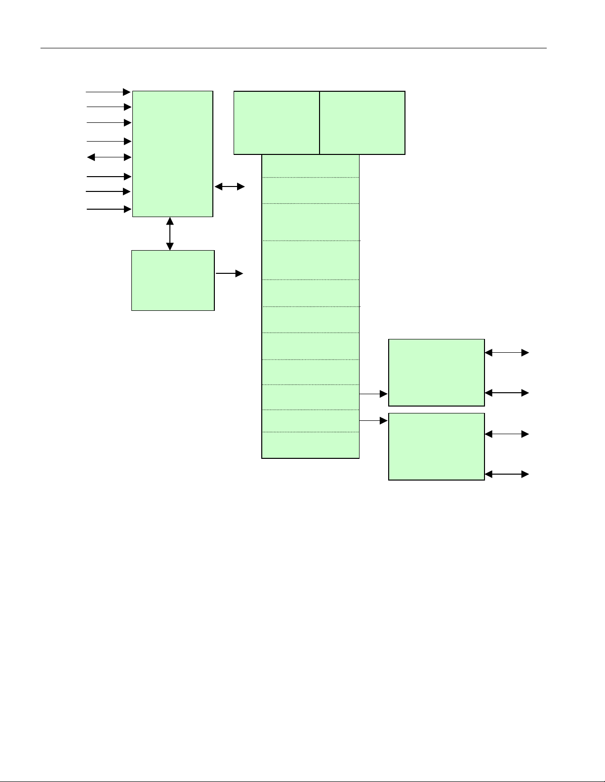
DS1847 BLOCK DIAGRAM Figure 1
A
WP
A0
A1
A2
SD
SCL
V
CC
Gnd
2-Wire
Interface
Digital
Temperature
Sensor
0h
47h
72x8 bit
EEPROM
Resistor 0
Look-up Table
(Table 1)
E0h
E1h
E2h
E3h
E4h
E5hE6h
E7h
E8hEFh
Resistor 0 Setting
F0h
F1h
F2hFFh
72x8 bit
EEPROM
Resistor 1
Look-up Table
(Table 2)
Table Select Byte
Configuration
Byte
Temperature
MSB Byte
Temperature
LSB Byte
Address Pointer
User Memory
Internal Address
Select
User Memory
Resistor 1 setting
User Memory
256 Position
Digitally-
Controlled
10kW or 50kW
Resistor 0
256 Position
Digitally-
Controlled 10kW
Resistor 1
DS1847
H0
L0
H1
L1
3 of 17
Page 4
DS1847
Memory
Name of Location Function of Location
Location
00h to 47h
(Table Select
Byte, E0h, must
be set to 01h or
02h to access the
Look-Up Tables)
User Defined Look-Up Table
(LUT)
This block contains the user defined temperature
settings of the resistors. Values between 00h and
FFh can be written to either table to set the 256
position variable resistors. The first address
location, 00h, is used to set the resistor at -40°C.
Each successive memory location will contain the
resistor setting for the previous temperature +2°C.
For example, memory address 01h is the address
that will set the resistor in a –38°C environment.
For default memory settings and programming
the look-up table, refer to the Programming the
Look-Up Table (LUT) section of the datasheet.
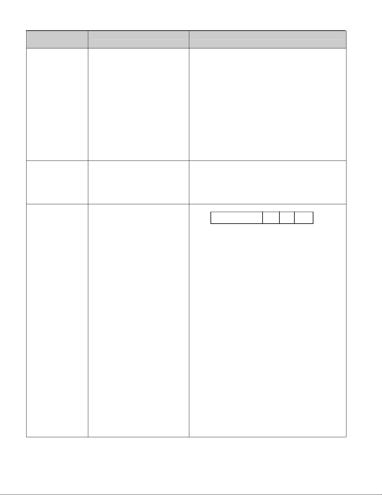
E0h Table Select Byte Writing to this byte determines which of the two
72x8 EEPROM look-up tables is selected for
reading or writing.
01h (Look-Up Table 1 selected)
02h (Look-Up Table 2 selected)
E1h Configuration Byte
TAU TEN AEN
TAU – Temperature/Address Update
TEN – Temperature Update Enable
AEN – Address Update Enable
Default setting is 03h, TAU = 1, TEN = 1 and
AEN = 1.
TAU becomes a 1 after a temperature and address
update has occurred as a result of a temperature
conversion. The user can write this bit to 0 and
check for a transition from 0 to 1 in order to
verify that a conversion has occurred.
If TEN = 0, the temperature conversion feature is
disabled. The user sets the resistor in “manual
mode” by writing to addresses F0h and
F1h to control resistors 0 and 1, respectively.
With AEN = 0 the user can operate in a test
mode. Address updates made from the
temperature sensor will cease. The user can load a
memory location into E4h and verify that the
values in locations F0h and F1h are the expected
user-defined values.
4 of 17
Page 5
DS1847
Memory
Name of Location Function of Location
Location
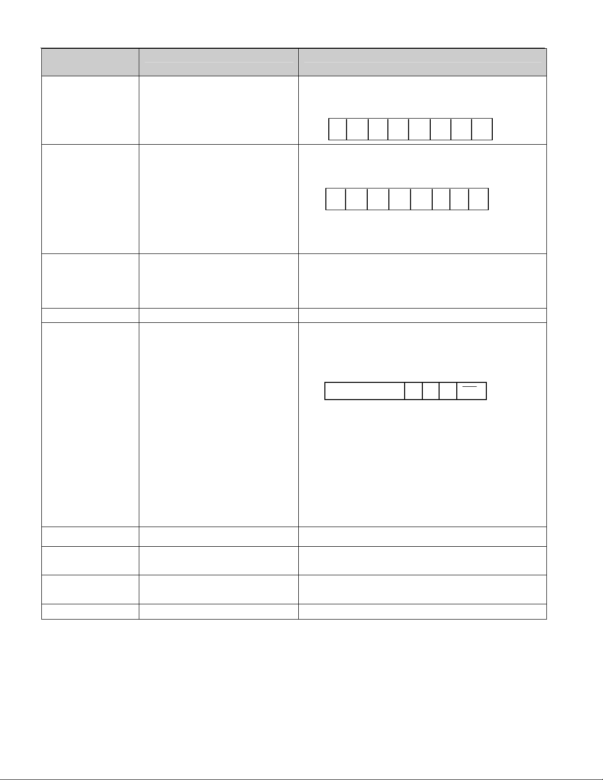
E2h Temperature MSB This byte contains the MSB of the 13-bit 2s
complement temperature output from the
temperature sensor.
S 27 26 25 24 23 22 21
E3h Temperature LSB This byte contains the LSB of the 13-bit 2s
complement temperature output from the
temperature sensor.
20 2-1 2-2 2-3 2-4 X X X
For example temperature readings, refer to Table
2.
E4h Address Pointer Calculated, current resistor address (0h – 47h).
The user-defined resistor setting at this location in
the respective look-up table will be loaded into
F0h and F1h to set the two resistors.
E5h to E6h User Memory General purpose user memory (SRAM)
E7h Address Select Internal or external device address select. This
byte allows the user to use the external address
pins or an internal register location to determine
the device address.
A2 A1 A0 ENB
ENB = 0 and external A2, A1, A0 grounded,
device will use internal address bits (A2, A1, A0)
in this register
ENB = 1, external A2, A1, A0 = any setting,
device will use external address pins
Default setting is 01h. The device uses external
pins to determine its address.
E8h to EFh User Memory General purpose user memory (SRAM)
F0h Resistor 0 Setting In the user-controlled setting mode, this block
contains the resistor 0 setting.
F1h Resistor 1 Setting In the user-controlled setting mode, this block
contains the resistor 1 setting.
F2h to FFh User memory General purpose user memory (SRAM)
5 of 17
Page 6
DS1847
[
]
PROGRAMMING THE LOOK-UP TABLE (LUT)
The following equation can be used to determine which resistor position setting, 00h – FFh, should be
written in the LUT to achieve a given resistance at a specific temperature.
),,(
CRpos
=
() ( ) ( )
[]
()()
CwCvuR
CzCyx
-·+-·+·
2
25251
-·+-·+·-
2
25251
aa -
DS1847-050
a = 3.78964 for the 50kW resistor
a = 19.74866 for the 10kW resistor
DS1847-010
a = 8.394533 for both 10kW resistors
R = resistance desired at the output terminal
C = temperature in degrees Celsius
u, v, w, x, y, and z are calibration constants programmed into each of the corresponding look-up tables.
Their addresses and LSB values are given in Table 1. Resistor 1 variables are found in Look-Up Table 1
of the EEPROM, and Resistor 2 variables are found in Look-Up Table 2. After these values are read, they
should be overwritten with the appropriate temperature-specific resistance settings.
LOOK-UP VARIABLE ADDRESSES Table 1
Address in
LUT (HEX)
28 – 29 u 2-8
2A – 2B v 10-6
2C – 2D w 10-9
2E – 2F x 2-8
30 – 31 y 10-7
32 – 33 z 10
When shipped from the factory, all other memory locations in the LUTs are programmed to FFh (except
bytes 00h-07h of Table 1 and 2 which may be factory programmed to values other than FFh).
Note: Memory locations 44h – 47h, which cover the temperature range (+96ºC to +102ºC), are outside
of the specified operating temperature range (-40ºC to +95ºC). However, the values stored in these
locations will act as valid resistance settings if the temperature exceeds +95ºC. Therefore, Dallas
Semiconductor recommends that the user programs a resistance value into all LUT locations. Failure to
do so will result in the part being set to the default value.
Variable LSB
-10
6 of 17
Page 7

DS1847
MEMORY LOCATION
TEMPERATURE CONVERSION
The direct-to-digital temperature sensor measures temperature through the use of an on-chip temperature
measurement technique with an operating range from -40°C to +95°C. Temperature conversions are
initiated upon power-up, and the most recent result is stored in address locations E2h and E3h, which are
updated every 10ms. Temperature conversion will not occur during an active read or write to memory.
The value of each resistor is determined by the temperature-addressed look-up table that assigns a unique
value to each resistor for every 2°C increment with a 1°C hysteresis at a temperature transition over the
operating temperature range. This can be seen in Figure 2.
TEMPERATURE CONVERSION HYSTERESIS Figure 2
M6
M5
M4
Increasing temp
Decreasing temp
M3
M2
M1
2 4 6 8 10 12
TEMPERATURE (C)
EXAMPLE TEMPERATURE READINGS Table 2
TEMP BINARY DATA HEX DATA
+95ºC 0010 1111 1000 0000 2F80h
+25.0625ºC 0000 1100 1000 1000 0C88h
-10.125ºC 1111 1010 1111 0000 FAF0h
-40ºC 1110 1100 0000 0000 EC00h
7 of 17
Page 8

DS1847
2-WIRE OPERATION
Clock and Data Transitions: The SDA pin is normally pulled high with an external resistor or device.
Data on the SDA pin may only change during SCL low time periods. Data changes during SCL high
periods will indicate a start or stop conditions depending on the conditions discussed below. Refer to the
timing diagram (Figure 4) for further details.
Start Condition: A high-to-low transition of SDA with SCL high is a start condition that must precede
any other command. Refer to the timing diagram (Figure 4) for further details.
Stop Condition: A low-to-high transition of SDA with SCL high is a stop condition. After a read
sequence, the stop command places the DS1847 into a low-power mode. Refer to the timing diagram
(Figure 4) for further details.
Acknowledge Bit: All address and data byte are transmitted via a serial protocol. The DS1847 pulls the
SDA line low during the ninth clock pulse to acknowledge that it has received each word.
Standby Mode: The DS1847 features a low-power mode that is automatically enabled after power-on,
after a stop command, and after the completion of all internal operations.
2-Wire Interface Reset: After any interruption in protocol, power loss, or system reset, the following
steps reset the DS1847:
1. Clock up to nine cycles.
2. Look for SDA high in each cycle while SCL is high.
3. Create a START condition while SDA is high.
Device Addressing: The DS1847 must receive an 8-bit device address word following a START
condition to enable a specific device for a read or write operation. The address word is clocked into the
DS1847 MSB to LSB. The address word consists of Ah (1010) followed by A2, A1, and A0 then the
R/W (READ/WRITE) bit. If the R/W bit is high, a read operation is initiated. If the R/W is low, a write
operation is initiated. For a device to become active, the values of A2, A1 and A0 must be the same as the
hard-wired address pins on the DS1847. Upon a match of written and hard-wired addresses, the DS1847
will output a zero for one clock cycle as an acknowledge. If the address does not match, the DS1847
returns to a low-power mode.
Write Operations: After receiving a matching address byte with the R/W bit set low, the device goes
into the write mode of operation. The master must transmit an 8-bit EEPROM memory address to the
device to define the address where the data is to be written. After this byte has been received, the DS1847
will transmit a zero for one clock cycle to acknowledge the receipt of the address. The master must then
transmit an 8-bit data word to be written into this address. The DS1847 will again transmit a zero for one
clock cycle to acknowledge the receipt of the data. At this point, the master must terminate the write
operation with a STOP condition. The DS1847 then enters an internally timed write process tw to the
EEPROM memory. All inputs are disabled during this byte write cycle.
The DS1847 is capable of an 8-byte page write. A page write is initiated the same way as a byte write, but
the master does not send a STOP condition after the first byte. Instead, after the slave acknowledges
receipt of the data byte, the master can send up to seven more bytes using the same nine-clock sequence.
8 of 17
Page 9

DS1847
The master must terminate the write cycle with a STOP condition or the data clocked into the DS1847
will not be latched into permanent memory.
Acknowledge Polling: Once the internally-timed write has started and the DS1847 inputs are disabled,
acknowledge polling can be initiated. The process involves transmitting a START condition followed by
the device address. The R/W bit signifies the type of operation that is desired. The read or write sequence
will only be allowed to proceed if the internal write cycle has completed and the DS1847 responds with a
zero.
Read Operations: After receiving a matching address byte with the R/W bit set high, the device goes
into the read mode of operation. There are three read operations: current address read, random read, and
sequential address read.
CURRENT ADDRESS READ
The DS1847 has an internal address register that maintains the address used during the last read or write
operation, incremented by one. This data is maintained as long as VCC is valid. If the most recent address
was the last byte in memory, then the register resets to the first address. This address stays valid between
operations as long as power is available.
Once the device address is clocked in and acknowledged by the DS1847 with the R/W bit set to high, the
current address data word is clocked out. The master does not respond with a zero, but does generate a
STOP condition afterwards.
RANDOM READ
A random read requires a dummy byte write sequence to load in the data word address. Once the device
and data address bytes are clocked in by the master and acknowledged by the DS1847, the master must
generate another START condition. The master now initiates a current address read by sending the device
address with the read/write bit set high. The DS1847 will acknowledge the device address and serially
clocks out the data byte.
SEQUENTIAL ADDRESS READ
Sequential reads are initiated by either a current address read or a random address read. After the master
receives the first data byte, the master responds with an acknowledge. As long as the DS1847 receives
this acknowledge after a byte is read, the master may clock out additional data words from the DS1847.
After reaching address FFh, it resets to address 00h.
The sequential read operation is terminated when the master initiates a stop condition. The master does
not respond with a zero.
For a more detailed description of 2-wire theory of operation, refer to the next section.
9 of 17
Page 10

DS1847
2-WIRE SERIAL PORT OPERATION
The 2-wire serial port interface supports a bi-directional data transmission protocol with device
addressing. A device that sends data on the bus is defined as a transmitter, and a device receiving data as
a receiver. The device that controls the message is called a “master.” The devices that are controlled by
the master are “slaves.” The bus must be controlled by a master device that generates the serial clock
(SCL), controls the bus access, and generates the START and STOP conditions. The DS1847 operates as
a slave on the 2-wire bus. Connections to the bus are made via the open-drain I/O lines SDA and SCL.
The following I/O terminals control the 2-wire serial port: SDA, SCL, A0, A1, A2. Timing diagrams for
the 2-wire serial port can be found in Figures 3 and 4. Timing information for the 2-wire serial port is
provided in the AC Electrical Characteristics Table for 2-wire serial communications.
The following bus protocol has been defined:
§ Data transfer may be initiated only when the bus is not busy.
§ During data transfer, the data line must remain stable whenever the clock line is HIGH. Changes in
the data line while the clock line is HIGH will be interpreted as control signals.
Accordingly, the following bus conditions have been defined:
Bus not busy: Both data and clock lines remain HIGH.
Start data transfer: A change in the state of the data line from HIGH to LOW while the clock is HIGH
defines a START condition.
Stop data transfer: A change in the state of the data line from LOW to HIGH while the clock line is
HIGH defines the STOP condition.
Data valid: The state of the data line represents valid data when, after a START condition, the data line
is stable for the duration of the HIGH period of the clock signal. The data on the line can be changed
during the LOW period of the clock signal. There is one clock pulse per bit of data. Figures 3 and 4 detail
how data transfer is accomplished on the 2-wire bus. Depending upon the state of the R/W bit, two types
of data transfer are possible.
Each data transfer is initiated with a START condition and terminated with a STOP condition. The
number of data bytes transferred between START and STOP conditions is not limited and is determined
by the master device. The information is transferred byte-wise and each receiver acknowledges with a
ninth bit.
Within the bus specifications a regular mode (100kHz clock rate) and a fast mode (400kHz clock rate) are
defined. The DS1847 works in both modes.
Acknowledge: Each receiving device, when addressed, is obliged to generate an acknowledge after the
reception of each byte. The master device must generate an extra clock pulse that is associated with this
acknowledge bit.
A device that acknowledges must pull down the SDA line during the acknowledge clock pulse in such a
way that the SDA line is a stable LOW during the HIGH period of the acknowledge-related clock pulse.
Of course, setup and hold times must be taken into account. A master must signal an end of data to the
10 of 17
Page 11

DS1847
slave by not generating an acknowledge bit on the last byte that has been clocked out of the slave. In this
case, the slave must leave the data line HIGH to enable the master to generate the STOP condition.
1. Data transfer from a master transmitter to a slave receiver. The first byte transmitted by the master is
the command/control byte. Next follows a number of data bytes. The slave returns an acknowledge bit
after each received byte.
2. Data transfer from a slave transmitter to a master receiver. The master transmits the first byte (the
command/control byte) to the slave. The slave then returns an acknowledge bit. Next, follows a
number of data bytes transmitted by the slave to the master. The master returns an acknowledge bit
after all received bytes other than the last byte. At the end of the last received byte, a ‘not
acknowledge’ can be returned.
The master device generates all serial clock pulses and the START and STOP conditions. A transfer is
ended with a STOP condition or with a repeated START condition. Since a repeated START condition is
also the beginning of the next serial transfer, the bus will not be released.
The DS1847 may operate in the following two modes:
1. Slave receiver mode: Serial data and clock are received through SDA and SCL, respectively. After
each byte is received, an acknowledge bit is transmitted. START and STOP conditions are recognized
as the beginning and end of a serial transfer. Address recognition is performed by hardware after
reception of the slave (device) address and direction bit.
2. Slave transmitter mode: The first byte is received and handled as in the slave receiver mode.
However, in this mode the direction bit will indicate that the transfer direction is reversed. Serial data
is transmitted on SDA by the DS1847, while the serial clock is input on SCL. START and STOP
conditions are recognized as the beginning and end of a serial transfer.
3. Slave Address: Command/control byte is the first byte received following the START condition from
the master device. The command/control byte consists of a 4-bit control code. For the DS1847, this is
set as 1010 binary for read/write operations. The next 3 bits of the command/ control byte are the
device select bits or slave address (A2, A1, A0). They are used by the master device to select which
of eight devices is to be accessed. When reading or writing the DS1847, the device-select bits must
match the device-select pins (A2, A1, A0). The last bit of the command/control byte (R/W) defines
the operation to be performed. When set to a 1, a read operation is selected, and when set to a 0, a
write operation is selected.
Following the START condition, the DS1847 monitors the SDA bus checking the device type identifier
being transmitted. Upon receiving the 1010 control code, the appropriate device address bits, and the
read/write bit, the slave device outputs an acknowledge signal on the SDA line.
WRITE PROTECT
The write-protect input pin (WP) protects all memory (including EEPROM), control registers, and lookup tables from alteration in an application. However, this does not interfere with internal
temperature/resistor updates. If set to a logic 0, the device is not write protected and can be written to via
the 2-wire interface. This pin has an internal pull-up resistor.
11 of 17
Page 12

2-WIRE DATA TRANSFER PROTOCOL Figure 3
2-WIRE AC CHARACTERISTICS Figure 4
DS1847
12 of 17
Page 13

DS1847
ABSOLUTE MAXIMUM RATINGS*
Voltage on Any Pin Relative to Ground -0.3V to +6.0V
Operating Temperature -40°C to +95°C
Programming Temperature 0°C to +70°C
Storage Temperature -55°C to +125°C
Soldering Temperature See J-STD-020A specification
* This is a stress rating only and functional operation of the device at these or any other conditions above
those indicated in the operation sections of this specification is not implied. Exposure to absolute
maximum rating conditions for extended periods of time may affect reliability.
RECOMMENDED DC OPERATING CONDITIONS (-40°C to +95°C)
PARAMETER SYMBOL CONDITION MIN TYP MAX UNITS NOTES
Supply Voltage Vcc +3.0 5.5 V 1
Resistor Inputs
Resistor Current I
L0, L1,
H0, H1
RESISTOR
DS1847-050
DS1847-010
GND-0.3
-1
-3
VCC+0.3
1
3
V
mA
DC ELECTRICAL CHARACTERISTICS (-40°C to +95°C; VCC = 3.0V to 5.5V)
PARAMETER SYMBOL CONDITION MIN TYP MAX UNITS NOTES
Supply Current
Input Leakage
(digital inputs)
Input Leakage (H0,
H1, L0, and L1)
Input Logic 1
Input Logic 0
Input Current each
I/O pin
ICC
IL
IL
VIH
VIL
0.4<V
0.5 1 mA 2
-1 +1 µA
-100 +100 nA
0.7VCC VCC+0.3 V 15
GND-0.3 0.3VCC V
<0.9VCC -10 +10
I/O
mA
13
3mA sink current 0.0 0.4 V Low Level Output
6mA sink current 0.0 0.6 V
10 pF
40 65 100
Voltage (SDA)
I/O Capacitance
WP Internal Pull Up
Resistance, R
wp
V
OL1
V
OL2
C
Rwp
I/O
13 of 17
kW
Page 14

DS1847
ANALOG RESISTOR CHARACTERISTICS (-40°C to +95°C; V
= 3.0V to 5.5V)
CC
PARAMETER SYMBOL CONDITION MIN TYP MAX UNITS NOTES
Absolute Error
Position FFh Resistance
DS1847-050
DS1847-050
DS1847-010
Position 00h Resistance
DS1847-050
DS1847-050
DS1847-010
using cal. values
(50k resistor)
(10k resistor)
(10k resistor)
(50k resistor)
(10k resistor)
(10k resistor)
-4 +4
44.6
9.0
8.0
500
500
250
55.8
11.3
10.0
850
850
425
67.0
13.6
12.0
1200
1200
600
LSB
kW
W
14
3
3
Absolute Linearity -2 +2 LSB 4
Relative Linearity -1 +1 LSB 5
Compensated Tempco
Error
using calibration
values
-4 +4 LSB 14
Uncompensated Tempco 850 ppm/°C 12
DIGITAL THERMOMETER
PARAMETER SYMBOL CONDITION TYP MAX UNITS NOTES
Thermometer Error T
-40°C to 95°C
ERR
±3.0 °C
Conversion Time t
12-bit conversion 10 ms
CONVT
14 of 17
Page 15

DS1847
AC ELECTRICAL CHARACTERISTICS (-40°C to +95°C, V
= 3.0V to 5.5V)
CC
PARAMETER SYMBOL CONDITION MIN TYP MAX UNITS NOTES
SCL clock frequency f
Bus free time between
STOP and START
Hold time (repeated)
START condition
Low period of SCL clock t
High period of SCL clock t
Data hold time t
Data set-up time t
Start set-up time t
Rise time of both SDA
and SCL signals
Fall time of both SDA
and SCL signals
Set-up time for STOP
condition
Capacitive load for each
Fast Mode
SCL
Standard Mode
t
Fast Mode
BUF
Standard Mode
t
Fast Mode
HD:STA
Standard Mode
Fast Mode
LOW
Standard Mode
Fast Mode
HIGH
Standard Mode
Fast Mode
HD:DAT
Standard Mode
Fast Mode
SU:DAT
Standard Mode
Fast Mode
SU:STA
Standard Mode
tR Fast Mode
Standard Mode
tF Fast Mode
Standard Mode
t
Fast Mode
SU:STO
Standard Mode
0
0
1.3
4.7
0.6
4.0
1.3
4.7
0.6
4.0
0
0
100
250
0.6
4.7
20+0.1CB
20+0.1CB
0.6
4.0
400
100
kHz 6
ms
6
ms
7, 6
ms
6
ms
6
0.9
ms
6, 8, 9
ns 6
ms
6
300
1000
300
300
ns 10
ns 10
ms
CB 400 pF 10
bus line
EEPROM write time tW 5 20 ms 11
NONVOLATILE MEMORY CHARACTERISTICS
PARAMETER SYMBOL CONDITION MIN TYP MAX UNITS
Writes 85°C 50,000
15 of 17
Page 16

DS1847
NOTES:
1. All voltages are referenced to ground.
2. Inputs SDA = SCL = WP = VCC. A0, A1, and A2, must be tied to VCC or GND.
3. Valid at 25°C only.
4. Absolute linearity is the difference of measured value from expected value at DAC position.
Expected value is a straight line from measured minimum position to measured maximum position.
5. Relative linearity is the deviation of an LSB DAC setting change vs. the expected LSB change.
Expected LSB change is the slope of the straight line from measured minimum position to measured
maximum position.
6. A fast mode device can be used in a standard mode system, but the requirement t
SU:DAT
then be met. This will automatically be the case if the device does not stretch the LOW period of the
SCL signal. If such a device does stretch the LOW period of the SCL signal, it must output the next
data bit to the SDA line t
RMAX
+ t
SU:DAT
= 1000ns + 250ns = 1250ns before the SCL line is released.
7. After this period, the first clock pulse is generated.
8. The maximum t
HD:DAT
has only to be met if the device does not stretch the LOW period (t
SCL signal.
9. A device must internally provide a hold time of at least 300ns for the SDA signal (referred to the
V
10. C
of the SCL signal) in order to bridge the undefined region of the falling edge of SCL.
IHMIN
– total capacitance of one bus line in picofarads, timing referenced to 0.9VCC and 0.1VCC.
B
11. EEPROM write begins after a STOP condition occurs.
12. The temperature coefficient varies with resistor position from 650ppm/°C at position FFh to
1000ppm/°C at 00h (for the 50k resistor), or 1500ppm/°C at 00h (for the 10k resistor). See the graphs
below. The tempco can be significantly reduced by using the resistor calibration values. When doing
so, the average tempco over the entire temperature range is between 200ppm°/C (for the lower
positions) and 10ppm/°C (higher positions). Refer to the Programming the Look-Up Table section of
the data sheet.
13. I/O pins of fast mode devices must not obstruct the SDA and SCL lines if VCC is switched off.
14. Refer to Programming the Look-Up Table section of the data sheet for calibration.
15. Address input A1 passes Latch-up per JEDEC 78 class I. All other pins pass class II.
> 250ns must
) of the
LOW
TEMPCO vs . RESISTANCE
10K RESISTOR
1500
1400
1300
1200
1100
1000
PPM/°C
900
800
700
600
500
0 2000 4000 6000 8000 10000
RESISTANCE (OHMS)
PPM/°C
1100
1000
900
800
700
600
500
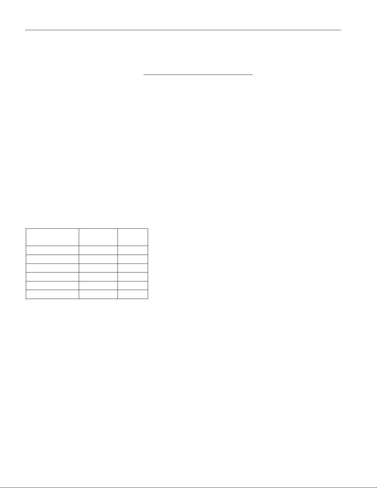
ORDERING INFORMATION
16 of 17
TEMPCO vs . RESISTANCE
50K RESISTOR
0 10000 20000 30000 40000 50 000
RESISTANCE (OHMS)
Page 17

ORDERING
NUMBER
PACKAGE OPERATING
TEMPERATURE
DS1847E-010 14-PIN TSSOP (173-MIL) -40ºC TO +95ºC
DS1847E-050 14-PIN TSSOP (173-MIL) -40ºC TO +95ºC
DS1847E-010/T&R 14-PIN TSSOP/TAPE & REEL -40ºC TO +95ºC
DS1847E-050/T&R 14-PIN TSSOP/TAPE & REEL -40ºC TO +95ºC
DS1847B-010 16-BALL CSBGA -40ºC TO +95ºC
DS1847B-050 16-BALL CSBGA -40ºC TO +95ºC
DS1847B-010+ 16-BALL CSBGA LF -40ºC TO +95ºC
DS1847B-010+T&R 16-BALL CSBGA LF T&R -40ºC TO +95ºC
DS1847B-010/T&R 16-BALL CSBGA T&R -40ºC TO +95ºC
DS1847B-050+ 16-BALL CSBGA LF -40ºC TO +95ºC
DS1847B-050+T&R 16-BALL CSBGA LF T&R -40ºC TO +95ºC
DS1847B-050/T&R 16-BALL CSBGA T&R -40ºC TO +95ºC
DS1847E-010+ 14-PIN TSSOP LF (173-MIL) -40ºC TO +95ºC
DS1847E-010+T&R 14-PIN TSSOP LF T&R -40ºC TO +95ºC
DS1847E-050+ 14-PIN TSSOP LF (173-MIL) -40ºC TO +95ºC
DS1847E-050+T&R 14-PIN TSSOP LF T&R -40ºC TO +95ºC
+ Denotes lead-free package.
DS1847
VERSION
Resistor 0
/Resistor 1
10kW/10kW
50kW/10kW
10kW/10kW
50kW/10kW
10kW/10kW
50kW/10kW
10kW/10kW
10kW/10kW
10kW/10kW
50kW/10kW
50kW/10kW
50kW/10kW
10kW/10kW
10kW/10kW
50kW/10kW
50kW/10kW
17 of 17
 Loading...