

Page 1
General Description
The DS1805 addressable digital potentiometer contains
a single 256-position digitally controlled potentiometer.
Device control is achieved through a 2-wire serial interface. Device addressing is provided through three
address inputs that allow up to eight devices on a single 2-wire bus. The exact wiper position of the potentiometer can be written or read. The DS1805 is
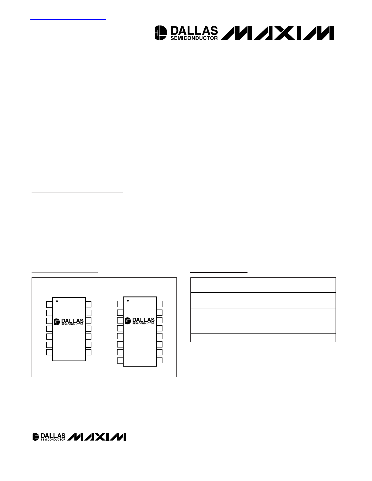
available in 16-pin SO and 14-pin TSSOP packages.
The device is available in three standard resistance values: 10kΩ, 50kΩ, and 100kΩ. The DS1805 is specified
over the industrial temperature range. The DS1805
provides a low-cost alternative for designs based on
the DS1803, but require only a single potentiometer.
Applications
CCFL Inverters
PDAs and Cell Phones
Portable Electronics
Multimedia Products
Instrumentation and Industrial Controls
Features
♦ 3V or 5V Operation
♦ Low Power Consumption
♦ One Digitally Controlled, 256-Position
Potentiometer
♦ Compatible with DS1803-Based Designs
♦ 14-Pin TSSOP (173mil) and 16-Pin SO (150mil)
Available for Surface-Mount Applications
♦ Three Address Inputs
♦ Serial 2-Wire Bus
♦ Operating Temperature Range
Industrial: -40°C to +85°C
♦ Standard Resistance Values
DS1805-010: 10kΩ
DS1805-050*: 50kΩ
DS1805-100*: 100kΩ
DS1805
Addressable Digital Potentiometer
______________________________________________ Maxim Integrated Products 1
14
13
12
11
10
9
8
1
2
3
4
5
6
7
V
CC
N.C.
N.C.
N.C.A2
W1
L1
H1
TOP VIEW
N.C.
SDA
SCLGND
A0
A1
14 TSSOP (173mil)
DS1805E
16
15
14
13
12
11
10
9
1
2
3
4
5
6
7
8
H1
V
CC
N.C.
N.C.
N.C.
N.C.
N.C.
SDA
SCL
16 SO (150mil)
N.C.
L1
A1
W1
A2
A0
GND
DS1805Z
Pin Configurations
Ordering Information
PART
TEM P RANGE
PIN- PACKAGE
RESISTANCE
( KΩ)
DS1805E-010
10
DS1805E-050*
50
DS1805E-100*
100
DS1805Z-010
16 SO (150mil) 10
DS1805Z-050*
16 SO (150mil) 50
DS1805Z-100*
16 SO (150mil) 10 0
XX-XXXX; Rev 0; 4/02
For pricing, delivery, and ordering information, please contact Maxim/Dallas Direct! at
1-888-629-4642, or visit Maxim’s website at www.maxim-ic.com.
Add “/T&R” for tape-and-reel orders.
*Future product.
查询DS1805E-010供应商
-40°C to +85°C 14 TSSOP (173mil)
-40°C to +85°C 14 TSSOP (173mil)
-40°C to +85°C 14 TSSOP (173mil)
-40°C to +85°C
-40°C to +85°C
-40°C to +85°C
Page 2
DS1805
Addressable Digital Potentiometer
2 _____________________________________________________________________
ABSOLUTE MAXIMUM RATINGS
RECOMMENDED DC OPERATING CONDITIONS
(TA= -40°C to +85°C)
Stresses beyond those listed under “Absolute Maximum Ratings” may cause permanent damage to the device. These are stress ratings only, and functional
operation of the device at these or any other conditions beyond those indicated in the operational sections of the specifications is not implied. Exposure to
absolute maximum rating conditions for extended periods may affect device reliability.
Voltage on Any Pin Relative to Ground .................-0.5V to +6.0V
Operating Temperature Range ...........................-40°C to +85°C
Storage Temperature Range .............................-55°C to +125°C
Soldering Temperature............................................See IPC/JEDEC
J-STD-020A Specification
PARAMETER
CONDITIONS
UNITS
Supply Voltage V
CC
(Note 1)
2.7 5.5 V
Resistor Inputs L, H, W (Note 1)
V
CC
+
0.3
V
DC ELECTRICAL CHARACTERISTICS
(VCC= 2.7V to 5.5V, TA= -40°C to +85°C.)
PARAMETER
CONDITIONS
UNITS
Supply Current Active I
CC
(Note 2) 200 µA
Input Leakage I
IL
-1 +1 µA
Wiper Resistance R
W
Ω
Wiper Current I
W
1mA
Input Logic 1 V
IH
V
CC
+
0.3
V
Input Logic 0 V
IL
GND -
0.3
V
Input logic 1
V
CC
+
0.3
Input Logic Levels A0, A1, A2
(Note 3)
Input logic 0
GND -
0.3
V
Input Current each I/O Pin
(Note 4)
0.4V < V
I/O
< 0.9V
CC
-10
µA
Standby Current I
STBY
(Note 5) 20 40 µA
V
OL1
3mA sink current 0 0.4 V
Low-Level Output Voltage
V
OL2
6mA sink current 0 0.6 V
I/O Capacitance C
I/0
10 pF
Pulse Width of Spikes that Must
be Suppressed by the Input Filter
t
SP
Fast mode 0 50 ns
SYMBOL
SYMBOL
MIN TYP MAX
-0.3
MIN TYP MAX
400 1000
0.7V
CC
0.7V
CC
0.3V
0 . 2 5 V
CC
C C
+10
Page 3
DS1805
Addressable Digital Potentiometer
_____________________________________________________________________ 3
ANALOG RESISTOR CHARACTERISTICS
(VCC= 2.7V to 5.5V, TA= -40°C to +85°C)
PARAMETER
SYMBOL
CONDITIONS
MIN
TYP
MAX
UNITS
End-to-End Resistor Tolerance (Note 6)
%
Absolute Linearity (Note 7)
LSB
Relative Linearity (Note 8)
LSB
-3dB Cutoff Frequency
(Note 9) Hz
Ratiometric Temperature Coefficient 8
ppm/°C
End-to-End Temperature Coefficient
ppm/°C
Capacitance
C
I
5pF
AC ELECTRICAL CHARACTERISTICS
(VCC= 2.7V to 5.5V, TA= -40°C to +85°C)
PARAMETER
CONDITIONS MIN
UNITS
Fast mode 0 400
SCL Clock Frequency (Note 10) f
SCL
Standard mode 0 100
kHz
Fast mode 1.3
Bus Free Time Between STOP
and START Condition (Note 10)
t
BUF
Standard mode 4.7
µs
Fast mode 0.6
Hold Time (Repeated) START
Condition (Notes 10, 11)
Standard mode 4.0
µs
Fast mode 1.3
Low Period of SCL Clock
(Note 10)
t
LOW
Standard mode 4.7
µs
Fast mode 0.6
High Period of SCL Clock
(Note 10)
t
HIGH
Standard mode 4.0
µs
Fast mode 0 0.9
Data Hold Time
(Notes 10, 12, 13)
Standard mode 0 0.9
µs
Fast mode 100
Data Setup Time
(Note 10)
Standard mode 250
ns
Fast mode
300
Rise Time of Both SDA and SCL
Signals (Notes 10, 14)
t
R
Standard mode
ns
Fast mode
300
Fall Time of Both SDA and SCL
Signals (Notes 10, 14)
t
F
Standard mode
300
ns
Fast mode 0.6
Setup Time for STOP Condition
(Note 10)
Standard mode 4.0
µs
Capacitive Load for Each Bus
Line (Note 14)
C
B
400 pF
f
CUTOFF
SYMBOL
t
HD:STA
-20 +20
-0.75 +0.75
-0.3 +0.3
550
TYP MAX
t
HD:DAT
t
SU:DAT
t
SU:STO
20 + 0.1C
20 + 0.1C
20 + 0.1C
20 + 0.1C
B
B
B
B
1000
Page 4

DS1805
Addressable Digital Potentiometer
4 _____________________________________________________________________
Note 1: All voltages are referenced to ground.
Note 2: I
CC
specified with SDA pin open. SCL = 400kHz clock rate.
Note 3: Address inputs A0, A1, and A2 should be connected to either V
CC
or GND, depending on the desired address selections.
Note 4: I/O pins of fast mode devices must not obstruct the SDA and SCL lines if V
CC
is switched off.
Note 5: I
STBY
specified with SDA = SCL = VCC= 5.0V.
Note 6: Valid at +25°C only.
Note 7: Absolute linearity is used to determine wiper voltage versus expected voltage as determined by wiper position.
Note 8: Relative linearity is used to determine the change in voltage between successive tap positions.
Note 9: -3dB cutoff frequency characteristics for the DS1805 depend on potentiometer total resistance: DS1805-010, 1MHz;
DS1805-50, 200kHz; DS1805-100, 100kHz.
Note 10: A fast mode device can be used in a standard mode system, but the requirement t
SU:DAT
> 250ns must then be met. This
will automatically be the case if the device does not stretch the low period of the SCL signal. If such a device does stretch
the LOW period of the SCL signal, it must output the next data bit to the SDA line t
RMAX
+ t
SU:DAT
= 1000ns + 250ns =
1250ns before the SCL line is released.
Note 11: After this period, the first clock pulse is generated.
Note 12: The maximum t
HD:DAT
has only to be met if the device does not stretch the low period (t
LOW
) of the SCL signal.
Note 13: A device must internally provide a hold time of at least 300ns for the SDA signal (referred to the V
IHMIN
of the SCL signal)
in order to bridge the undefined region of the falling edge of SCL.
Note 14: C
B
—total capacitance of one bus line in picofarads, timing referenced to (0.9)(VCC) and (0.1)(VCC).
AC ELECTRICAL CHARACTERISTICS
(VCC= 2.7V to 5.5V, TA= -40°C to +85°C)
Page 5

Typical Operating Characteristics
(VCC= 5.0V, TA= +25°C, unless otherwise noted.)
DS1805
Addressable Digital Potentiometer
_____________________________________________________________________ 5
VOLTAGE-DIVIDER ABSOLUTE LINEARITY
vs. WIPER SETTING (10kΩ)
DS1805 toc07
WIPER SETTING
ABSOLUTE LINEARITY (LSB)
20015050 100
0.04
0.06
0.08
0.10
0.12
0.14
0.16
0.18
0
0.02
0 250
VOLTAGE-DIVIDER RELATIVE LINEARITY
vs. WIPER SETTING (10kΩ)
DS1805 toc08
WIPER SETTING
RELATIVE LINEARITY (LSB)
20015010050
0
0.01
0.02
0.03
0.04
0.05
0.06
-0.01
0 250
ACTIVE SUPPLY CURRENT
vs. SCL FREQUENCY
DS1805 toc06
SCL FREQUENCY (kHz)
ACTIVE SUPPLY CURRENT (µA)
300200100
5
10
15
20
25
30
35
40
45
50
0
0 400
SDA = VCC
A0, A1, A2, L1 = GND
W1, H1 = NO CONNECT
END-TO-END RESISTANCE TEMPERATURE
CHANGE vs. TEMPERATURE
DS1805 toc05
TEMPERATURE (°C)
END-TO-END RESISTANCE % CHANGE
6040-20 0 20
-4
-3
-2
-1
0
1
2
3
4
5
-5
-40 80
TC = 530ppm/°C
10kΩ, WORST CASE
VOLTAGE DIVIDER PERCENT CHANGE
(FROM +25°C) vs. TEMPERATURE
(RATIOMETRIC TC)
DS1805 toc04
TEMPERATURE (°C)
% CHANGE (FROM +25°C)
6040200-20
-0.04
-0.02
0
0.02
0.04
0.06
-0.06
-40 80
10kΩ POT
WIPER = BFh
WIPER = BFh
WIPER = 3Fh
WIPER = 3Fh
WIPER = 7Fh
TC = 1.3ppm/°C
TC = 8.1ppm/°C
WIPER RESISTANCE vs.
WIPER VOLTAGE (10kΩ)
DS1805 toc03
WIPER VOLTAGE (V)
WIPER RESISTANCE (Ω)
4321
50
100
150
200
250
300
350
0
05
VCC = 3V
VCC = 5V
W-L RESISTANCE
vs. WIPER SETTING
DS1805 toc02
WIPER SETTING
W-L RESISTANCE (kΩ)
225200175150125100755025
2
4
6
8
10
0
0 250
10kΩ POTENTIOMETER
SUPPLY CURRENT
vs. TEMPERATURE
DS1805 toc01
TEMPERATURE (°C)
SUPPLY CURRENT (µA)
6040200-20
5
10
15
20
25
30
0
-40 80
VCC = 5V
VCC = 3V
Page 6

DS1805
Addressable Digital Potentiometer
6 _____________________________________________________________________
Detailed Description
The DS1805 addressable digital potentiometer contains a
single 256-position digitally controlled potentiometer.
Device control is achieved through a 2-wire serial interface. Device addressing is provided through three
address inputs that allow up to eight devices on a single
2-wire bus. The exact wiper position of the potentiometer
can be written or read. The DS1805 is available in 16-pin
SO and 14-pin TSSOP packages. The device is available
in three standard resistance values: 10kΩ, 50kΩ, and
100kΩ. The DS1805 specified over the industrial temperature range. The DS1805 is provides a low-cost alternative for designs based on the DS1803, but require only a
single potentiometer.
Device Operation
The DS1805 is an addressable, digitally controlled
device that has a single 256-position potentiometer.
Figure 1 shows a block diagram of the part.
Communication and control of the device is accomplished through a 2-wire serial interface that has SDA
and SDL signals. Device addressing is attained using
the device chip-select inputs A0, A1, and A2.
W1
SCL
SDA
A0
A1
A2
2-WIRE SERIAL
INTERFACE
REG-0 (8-BIT REGISTER)
SRAM
WIPER-1 (8-BIT REGISTER)
COMMAND/
CONTROL
UNIT
DEVICE ADDRESS
SELECTION
L1
256-TO-1 MULTIPLEXER
POTENTIOMETER-1
H1
Figure 1. Functional Diagram
PIN
TSSOP
SO
NAME FUNCTION
11 H1
High End of
Potentiometer
23 L1
Low End of
Potentiometer
34 W1
Wiper Terminal of
Potentiometer
6, 5, 4
7, 6, 5
Address Select Inputs
78 GND Ground
89 SCL Serial Clock Input
910 SDA Serial Data I/O
10–13
N.C. No Connection
14 16 V
CC
3V/5V Power-Supply
Input
Pin Description
A0, A1, A2
2, 11–15
Page 7

DS1805
Addressable Digital Potentiometer
_____________________________________________________________________ 7
The potentiometer is composed of a 256-position resistor array. Two 8-bit registers are provided to ensure
compatibility with DS1803-based designs. Register-0 is
a general-purpose SRAM byte, while register-1 is
assigned to the potentiometer and is used to set the
wiper position on the resistor array. The wiper terminal
is multiplexed to one of 256 positions on the resistor array
based on its corresponding 8-bit register value. The highest wiper setting, FFh, is 1 LSB away from H1 (resistor
255), while the lowest setting, 00h, connects to L1.
The DS1805 is a volatile device that does not maintain
the position of the wiper during power-down or loss of
power. On power-up, the wiper position is set to 00h
(the low-end terminal). The user can then set the wiper
value to a desired position.
Communication with the DS1805 takes place over the
2-wire serial interface consisting of the bidirectional
data terminal, SDA, and the serial clock input, SCL.
Complete details of the 2-wire interface are discussed
in the 2-Wire Serial Data Bus section.
The 2-wire interface and address inputs A0, A1, and A2
allow operation of up to eight devices in a bus topology,
with A0, A1, and A2 being the address of the device.
Application Considerations
The DS1805 is offered in three standard resistor values:
10kΩ, 50kΩ, and 100kΩ. The resolution of the potentiometer is defined as R
TOT
/256, where R
TOT
is the total
resistor value of the potentiometer. The DS1805 is
designed to operate using 3V or 5V power supplies over
the industrial (-40°C to +85°C) temperature range.
Maximum input signal levels across the potentiometer
cannot exceed the operating power supply of the device.
2-Wire Serial Data Bus
The DS1805 supports a bidirectional 2-wire bus and
data transmission protocol. A device that sends data on
the bus is called a transmitter, and a device receiving
data is called a receiver. The device that controls the
message is called a master. The devices that are controlled by the master are slaves. The bus must be controlled by a master device that generates the serial
clock (SCL), controls the bus access, and generates the
START and STOP conditions. The DS1805 operates as
a slave on the 2-wire bus. Connections to the bus are
made through the open-drain I/O lines, SDA and SCL.
The following bus protocol has been defined (Figure 2):
• Data transfer can be initiated only when the bus is
not busy.
• During data transfer, the data line must remain stable whenever the clock line is high. Changes in the
data line while the clock line is high will be interpreted as control signals.
Accordingly, the following bus conditions have been
defined:
Bus not busy: Both data and clock lines remain high.
Start data transfer: A change in the state of the data
line from high to low while the clock is high defines a
START condition.
STOP
CONDITION
OR REPEATED
START
CONDITION
REPEATED IF MORE BYTES
ARE TRANSFERED
ACK
START
CONDITION
ACK
ACKNOWLEDGEMENT
SIGNAL FROM RECEIVER
ACKNOWLEDGEMENT
SIGNAL FROM RECEIVER
SLAVE ADDRESS
MSB
SCL
SDA
R/W
DIRECTION
BIT
12 678 9 12 893–7
Figure 2. 2-Wire Data Transfer Overview
Page 8

DS1805
Addressable Digital Potentiometer
8 _____________________________________________________________________
Stop data transfer: A change in the state of the data
line from low to high while the clock line is high defines
the STOP condition.
Data valid: The state of the data line represents valid
data when, after a START condition, the data line is stable for the duration of the high period of the clock signal.
The data on the line must be changed during the low
period of the clock signal. There is one clock pulse per
bit of data. Figure 2 details how data transfer is accomplished on the 2-wire bus. Depending upon the state of
the R/W bit, two types of data transfer are possible.
Each data transfer is initiated with a START condition
and terminated with a STOP condition. The number of
data bytes transferred between START and STOP conditions is not limited and is determined by the master
device. The information is transferred byte-wise and
each receiver acknowledges with a ninth bit.
Within the bus specifications a regular mode (100kHz
clock rate) and a fast mode (400kHz clock rate) are
defined. The DS1805 works in both modes.
Acknowledge: Each receiving device, when addressed,
is obliged to generate an acknowledge after the reception of each byte. The master device must generate an
extra clock pulse that is associated with this acknowledge bit.
A device that acknowledges must pull down the SDA
line during the acknowledge clock pulse in such a way
that the SDA line is stable low during the high period of
the acknowledge-related clock pulse. Of course, setup
and hold times must be taken into account. A master
must signal an end of data to the slave by not generating an acknowledge bit on the last byte that has been
clocked out of the slave. In this case, the slave must
leave the data line high to enable the master to generate the STOP condition.
Data transfer from a master transmitter to a slave
receiver: The first byte transmitted by the master is the
control byte (slave address). Next follows a number of
data bytes. The slave returns an acknowledge bit after
each received byte.
Data transfer from a slave transmitter to a master
receiver: The first byte (the slave address) is transmit-
ted by the master. The slave then returns an acknowledge bit. Next follows a number of data bytes
transmitted by the slave to the master. The master
returns an acknowledge bit after all received bytes
other than the last byte. At the end of the last received
byte, a ‘not acknowledge’ is returned.
The master device generates all of the serial clock
pulses and the START and STOP conditions. A transfer
is ended with a STOP condition or with a repeated
START condition. Since a repeated START condition is
also the beginning of the next serial transfer, the bus
will not be released.
The DS1805 can operate in the following two modes:
Slave receiver mode: Serial data and clock are
received through SDA and SCL. After each byte is
received, an acknowledge bit is transmitted. START and
STOP conditions are recognized as the beginning and
end of a serial transfer. Address recognition is performed
by hardware after reception of the slave address and
direction bit.
Slave transmitter mode: The first byte is received and
handled as in the slave receiver mode. However, in this
mode the direction bit will indicate that the transfer
direction is reversed. Serial data is transmitted on SDA
by the DS1805 while the serial clock is input on SCL.
START and STOP conditions are recognized as the
beginning and end of a serial transfer.
Slave Address
A control byte is the first byte received following the
START condition from the master device. The control
byte consists of a four-bit control code; for the DS1805,
this is set as 0101 binary for read/write operations. The
next three bits of the control byte are the device select
bits (A2, A1, A0). They are used by the master device
to select which of eight devices are to be accessed.
The select bits are the three least significant bits (LSB)
of the slave address. Additionally, A2, A1, and A0 can
be changed any time during a powered condition of the
part. The last bit of the control byte (R/W) defines the
operation to be performed. When set to a one, a read
operation is selected; when set to a zero a write operation is selected. Figure 3 shows the control byte structure for the DS1805.
Figure 3. Control Byte
MSB
DEVICE
IDENTIFIER
DEVICE
ADDRESS
READ/WRITE BIT
0 101A2A1 A0 R/W
LSB
Page 9

DS1805
Addressable Digital Potentiometer
_____________________________________________________________________ 9
Following the START condition, the DS1805 monitors
the SDA bus checking the device type identifier being
transmitted. Upon receiving the 0101 address code
and appropriate device select bits, the slave device
outputs an acknowledge signal on the SDA line.
Command and Protocol
The DS1805’s command and protocol structure of the
DS1805 allows the user to read or write to both the
scratchpad and potentiometer registers. Figures 4 and
5 show the command structures for the part.
Potentiometer data values and control and command
values are always transmitted most significant bit
(MSB) first. During communications, the receiving unit
always generates the acknowledge.
Reading the DS1805
As shown in Figure 4, the DS1805 provides one readcommand operation. This operation allows the user to
read both potentiometers. Specifically, the R/W bit of the
control byte is set equal to a one for a read operation.
Communication to read the DS1805 begins with a START
condition that is issued by the master device. The control
byte from the master device follows the START condition.
Once the control byte has been received by the DS1805,
the part responds with an acknowledge. The read/write
bit of the control byte as stated should be set equal to
one for reading the DS1805.
When the master has received the acknowledge from the
DS1805, the master can then begin to receive potentiometer wiper data. The value of the register-0 wiper
position will be the first returned from the DS1805. Once
the eight bits of the register-0 wiper position have been
transmitted, the master needs to issue an acknowledge,
unless it is the only byte to be read, in which case the
master issues a not acknowledge. If desired, the master
can stop the communication transfer at this point by issuing the STOP condition. However, if the value of the
potentiometer-1 wiper position value is needed, commu-
nication transfer can continue by clocking the remaining
eight bits of the potentiometer-1 value, followed by a not
acknowledge. Final communication transfer is terminated
by issuing the STOP command. Figure 4 shows the flow
of the read operation.
Writing to the DS1805
Figure 5 shows a data flow diagram for writing the
DS1805. The DS1805 has three write-command operations. These include write reg-0, write pot-1, and write
reg-0/pot-1. The write reg-0 command allows the user to
write the value of scratchpad register-0 and as an option
the value of potentiometer-1. The write-1 command allows
the user to write the value of potentiometer-1 only. The
last write command, write-0/1, allows the user to write
both registers to the same value with one command and
one data value being issued.
All the write operations begin with a START condition.
Following the START condition, the master device issues
the control byte. The read/write bit of the control byte is
set to zero for writing the DS1805. Once the control byte
has been issued and the master receives the acknowledgment from the DS1805, the command byte is transmitted to the DS1805. As mentioned above, there exist
three write operations that can be used with the DS1805.
Figure 5 and Table 1 show the binary value of each write
command.
Figure 4. 2-Wire Read Protocols
MSB
START
ACK
ACK
ACK
STOP
CONTROL
BYTE
LSB MSB
DATA
BYTE
LSB MSB
OPTIONAL
DATA
BYTE
LSB
REG-0 POT-1
R/W = 1
0101A2A1 A0 1
Table 1. 2-Wire Command Words
Package Information
For the latest package outline information, go to
www.maxim-ic.com/packages.
Write Register-0 101010 01
Write Potentiometer-1 Register 101010 10
Write Both Registers 101011 11
COMMAND COMMAND VALUE
Page 10

DS1805
Addressable Digital Potentiometer
Maxim cannot assume responsibility for use of any circuitry other than circuitry entirely embodied in a Maxim product. No circuit patent licenses are
implied. Maxim reserves the right to change the circuitry and specifications without notice at any time.
10 ____________________Maxim Integrated Products, 120 San Gabriel Drive, Sunnyvale, CA 94086 408-737-7600
© 2002 Maxim Integrated Products Printed USA is a registered trademark of Maxim Integrated Products.
Figure 5. 2-Wire Write Protocols
Figure 6. Timing Diagram
ACK
STOP
MSB
OPTIONAL
DATA
BYTE
LSB
POT-1
MSB
START
ACK
ACK
ACK
STOP
CONTROL
BYTE
LSB MSB
COMMAND
BYTE
LSB MSB
DATA
BYTE
LSB
POT-1
R/W = 0
MSB
REGISTER-0
WRITE POT-1
WRITE REGISTER-0 AND POT-1 (SAME VALUE)
START
ACK
ACK
ACK
CONTROL
BYTE
LSB MSB
COMMAND
BYTE
LSB MSB
DATA
BYTE
LSB
REG-0
R/W = 0
0101A2A1 A0 0
0101A2A1 A0 0
0101A2A1 A0 0
10101001
10101010
MSB
START
ACK
ACK
ACK
STOP
CONTROL
BYTE
LSB MSB
COMMAND
BYTE
LSB MSB
DATA
BYTE
LSB
REG-0/POT-1 VALUE
R/W = 0
10101111
SDA
SCL
t
BUF
STOP START
t
LOW
t
HD:STA
t
R
t
HD:DAT
t
F
t
HIGH
t
SU:DAT
REPEATED
START
t
HD:STA
t
SU:STA
t
SP
t
SU:STO
 Loading...