

V
μ
RST
Q
www.maxim-ic.com
DESCRIPTION
The DS1626 and DS1726 digital
thermometers/thermostats provide temperature
measurements and stand-alone thermostat
capability over a -55°C to +125°C range. The
DS1626 offers ±0.5°C accuracy from 0°C to
+70°C and the DS1726 has ±1°C accuracy from
-10°C to +85°C. The resolution of the measured
temperature is user selectable from 9 to 12 bits.
Communication with the DS1626 and DS1726 is
achieved through a 3-wire serial bus.
The DS1626 and DS1726 offer thermostatic
functionality with three dedicated thermostat
outputs (T
HIGH
, T
, and T
LOW
), and
COM
overtemperature (TH) and undertemperature (TL)
user-programmable thresholds stored in on-chip
EEPROM. For stand-alone thermostat operation,
TH and TL can be programmed prior to
installation, and the DS1626/DS1726 can be
configured to automatically begin taking
temperature measurements at power-up. Table 1
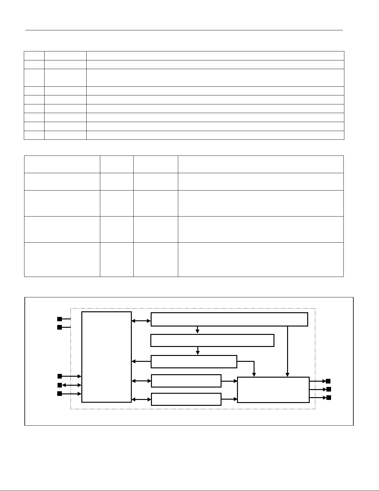
summarizes the user-accessible registers. Figure
1 shows a functional diagram.
APPLICATIONS
Thermostatic Controls
Industrial Controls
Consumer Products
Any Space-Constrained Thermally Sensitive
Application
High-Precision 3-Wire Digital
Thermometer and Thermostat
FEATURES
Temperature Measurements Require No
External Components
Measure Temperatures from -55°C to
+125°C (-67°F to +257°F)
DS1626: ±0.5°C Accuracy from 0°C to
+70°C
DS1726: ±1°C Accuracy from -10°C to
+85°C
Output Resolution is User Selectable to 9,
10, 11, or 12 Bits
Wide Power-Supply Range (2.7V to 5.5V)
Convert Temperature to Digital Word in
750ms (max)
Stand-Alone Thermostat Capability
Thermostatic Settings are User Definable and
Nonvolatile (NV)
Data is Read/Written Through a 3-Wire
Serial Interface
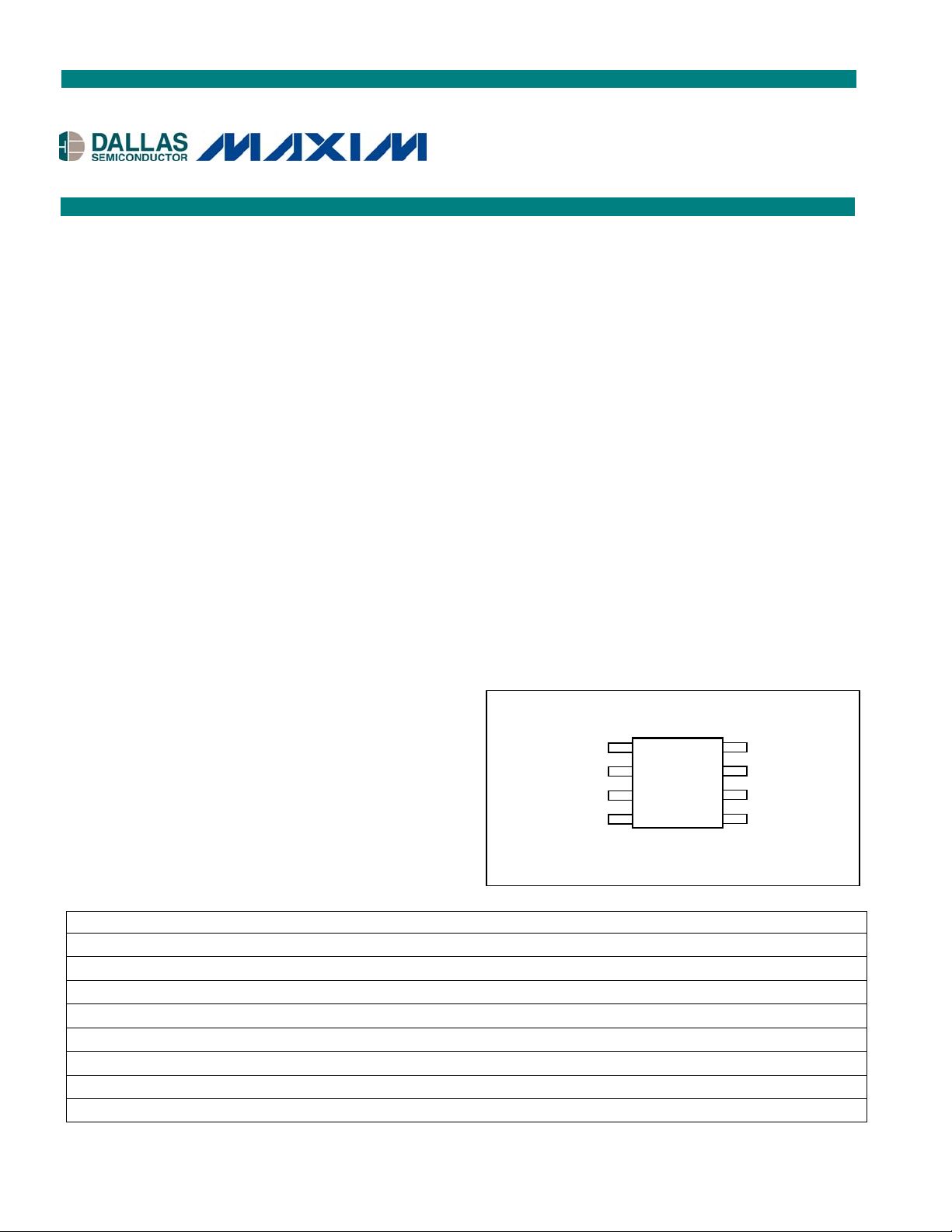
Available in 8-Pin μSOP Package
PIN CONFIGURATION
TOP VIEW
D
CLK/CN
GND
ORDERING INFORMATION
PART TEMP RANGE PIN-PACKAGE TOP MARK
DS1626U -55°C to +125°C
DS1626U+ -55°C to +125°C
DS1626U/T&R -55°C to +125°C
DS1626U+T&R -55°C to +125°C
DS1726U -55°C to +125°C
DS1726U+ -55°C to +125°C
DS1726U/T&R -55°C to +125°C
DS1726U+T&R -55°C to +125°C
+Denotes a lead-free package. A “+” symbol will also be marked on the package near the Pin 1 indicator.
T&R = Tape and reel.
8 μSOP
8 μSOP
8 μSOP, 3000-Piece
8 μSOP, 3000-Piece
8 μSOP
8 μSOP
8 μSOP, 3000-Piece
8 μSOP, 3000-Piece
DS1626/DS1726
VDD
7
T
HIGH
6
T
LOW
T
COM
1626
1626
1626
1626
1726
1726
1726
1726
2
3
DS1626
DS1726
SOP
1 of 12 REV: 071107
CNV
R
PIN DESCRIPTION
PIN NAME FUNCTION
1 DQ Data Input/Output Pin (Tri-State) for 3-Wire Serial Communication
2
3
CLK/CNV
RST
Clock Input Pin for 3-Wire Serial Communication. Controls temperature
measurements when the DS1626/DS1726 is configured as a stand-alone thermostat.
Reset Input Pin for 3-Wire Serial Communication
4 GND Ground Pin
5 T
6 T
7 T
Thermostat Output Pin (Push-Pull) with Programmable Hysteresis
COM
Thermostat Output Pin (Push-Pull) with TL Trip Point
LOW
Thermostat Output Pin (Push-Pull) with TH Trip Point
HIGH
8 VDD Supply Voltage. +2.7V to +5.5V input power pin.
Table 1. DS1626/DS1726 REGISTER SUMMARY
REGISTER NAME
(USER ACCESS)
Temperature
(Read Only)
T
H
(Read/Write)
T
L
(Read/Write)
Configuration
(Various Bits are
Read/Write and Read
Only—See Table 3)
SIZE
12 Bits SRAM
12 Bits EEPROM
12 Bits EEPROM
1 Byte
MEMORY
TYPE
SRAM and
EEPROM
REGISTER CONTENTS
AND POWER-UP/POR STATE
Measured Temperature (Two’s Complement)
Power-Up/POR State: -60ºC (1100 0100 0000)
Upper Alarm Trip Point (Two’s Complement)
Power-Up/POR State: User Defined
Initial State from Factory: +15°C (0000 1111 0000)
Lower Alarm Trip Point (Two’s Complement)
Power-Up/POR State: User Defined
Initial State from Factory: +10°C (0000 1010 0000)
Configuration and Status Information (Unsigned)
4MSbs = SRAM and 4LSbs = EEPROM
Power-Up/POR State: 1000XXXX (XXXX = User
Defined)
Figure 1. DS1626/DS1726 FUNCTIONAL DIAGRAM
VDD
CONFIGURATION REGISTER AND CONTROL LOGIC
CLK/
ADDRESS
and
I/O CONTROL
SDA
ST
TEMPERATURE SENSOR AND ΔΣ ADC
TEMPERATURE REGISTER
T
REGISTER
H
COMPARATOR/LOGIC
TL REGISTER
DIGITAL
DS1626/DS1726
T
T
T
LOW
2 of 12
DS1626/DS1726
ABSOLUTE MAXIMUM RATINGS
Voltage Range on Any Pin Relative to Ground...................................................................-0.5V to +6.0V
Operating Temperature Range.............................................................................................-55°C to +125°C
Storage Temperature Range ................................................................................................-55°C to +125°C
Solder Dip Temperature (10s).............................................................................................+260°C
Reflow Oven Temperature ..................................................................................................+220°C
These are stress ratings only and functional operation of the device at these or any other conditions above those indicated in the operation
sections of this specification is not implied. Exposure to absolute maximum rating conditions for extended periods of time may affect
reliability.
DC ELECTRICAL CHARACTERISTICS
(V
= 2.7V to 5.5V, TA = -55°C to +125°C.)
DD
PARAMETER SYMBOL CONDITIONS MIN TYP MAX UNITS
Supply Voltage VDD
DS1626
Thermometer
Error
T
ERR
(Note 2)
DS1726
Thermometer
T
ERR
Error (Note 2)
Low-Level Input
Voltage
High-Level Input
Voltage
Input Current
each Input Pin
Active Supply
Current (Note 3)
VIL (Note 1) -0.5 0.3 x V
VIH (Note 1) 0.7 x V
0.4 < V
I
DD
Input Resistance RI
Standby Supply
Current
I
STBY
VOH 1mA source current 2.4 THIGH, TLOW,
TCOM, DQ
Output Logic
V
OL
Voltages (Note 1)
Thermal Drift
0°C to +70°C (Note 3) 1.5 µA
4mA sink current 0.4
(Note 1) 2.7 5.5 V
0°C to +70°C,
3.0V ≤ V
≤ 5.5V
DD
0°C to +70°C,
2.7V ≤ V
< 3.0V
DD
-55°C to +125°C
-10°C to +85°C,
3.0V ≤ V
≤ 5.5V
DD
-10°C to +85°C,
2.7V ≤ V
< 3.0V
DD
±0.5
±1.25
±1.5
°C
±2
±1
°C
-55°C to +125°C ±2
V
mA
< 0.9 x VDD -10 +10 µA
I/O
Temperature conversion
-55°C to +85°C
Temperature conversion
+85°C to +125°C
DD
DD
V
+ 0.3 V
DD
1
1.25
E2 write 400 µA
RST to GND
DQ, CLK to V
DD
1
MΩ
V
(Note 4)
±0.2 °C
3 of 12
DS1626/DS1726
EEPROM AC ELECTRICAL CHARACTERISTICS
= 2.7V to 5.5V, TA = -55°C to +125°C.)
(V
DD
PARAMETER SYMBOL CONDITIONS MIN TYP MAX UNITS
EEPROM Write Cycle Time twr 4 10 ms
EEPROM Writes N
EEPROM Data Retention t
-55°C to +55°C 50k Writes
EEWR
-55°C to +55°C 10 Years
EEDR
AC ELECTRICAL CHARACTERISTICS
(V
= 2.7V to 5.5V, TA = -55°C to +125°C.)
DD
PARAMETER SYMBOL CONDITIONS MIN TYP MAX UNITS
9 bits 93.75
Temperature Conversion Time tTC
10 bits 187.5
11 bits 375
ms
12 bits 750
Data In to Clock Setup tDC (Note 5) 35 ns
Clock to Data In Hold t
Clock to Data Out Delay t
(Note 5) 40 ns
CDH
(Notes 5, 6) 150 ns
CDD
Clock Low/High Time tCL, tCH (Note 5) 285 ns
Clock Frequency f
(Note 5) 0 1.75 MHz
CLK
Clock Rise/Fall Time tR, tF (Note 5) 500 ns
RST to Clock Setup
Clock to RST Hold
RST Inactive Time
Clock High to I/O Hi-Z t
RST Low to I/O Hi-Z
CNV Pulse Width
I/O Capacitance C
tRC (Note 5) 100 ns
t
(Note 5) 40 ns
CRH
tRI (Note 7) 125 ns
(Note 5) 50 ns
CDZ
t
(Note 5) 50 ns
RDZ
t
(Note 8) 250ns 500ms
CNV
I/O
10 pF
Input Capacitance CI 5 pF
NOTES:
1) All voltages are referenced to ground.
2) See Figure 2 for TYPICAL OPERATING CURVES.
3) I
4) Drift data is based on a 1000hr stress test at +125°C with V
5) See Timing Diagrams in Figure 3. All timing is referenced to 0.7 x V
6) Load capacitance = 50pF.
7) tRI must be 10ms minimum following any write command that involves the E2 memory.
8) 250ns is the guaranteed minimum pulse width for a conversion to start, however, a smaller pulse
, IDD specified with DQ, CLK/CNV = VDD and RST = GND.
STBY
width may start a conversion.
= 5.5V.
DD
and 0.3 x VDD.
DD
4 of 12

Figure 2. TYPICAL OPERATING CURVES
0.8
0.6
0.4
0.2
+3σ
0
-0.2
-0.4
ERROR °C
-0.6
-3σ
-0.8
-1
0 10203040506070
REFERENCE TEMPERATURE (°C)
DS1626
MEAN
Figure 3. TIMING DIAGRAMS
a) Read Timing
tRC
DS1726
0.8
0.6
0.4
0.2
0
-0.2
-0.4
-0.6
ERROR (°C)
-0.8
MEAN
-1
-10 0 10 20 30 40 50 60 70 80
REFERENCE TEMPERATURE (°C)
t
CRH
DS1626/DS1726
+3σ
-3σ
b) Write Timing
tRC
5 of 12
tRI
t
CRH

DS1626/DS1726
OPERATION—MEASURING TEMPERATURE
The DS1626/DS1726 measure temperature using a bandgap-based temperature sensor. A delta-sigma
analog-to-digital converter (ADC) converts the measured temperature to a digital value that is calibrated
in degrees Celsius; for Fahrenheit applications a lookup table or conversion routine must be used.
Communication with the DS1626/DS1726 is achieved through a 3-wire serial interface, and all data is
transmitted LSb first.
The DS1626/DS1726 can be programmed to take continuous temperature measurements (continuous
conversion mode) or to take single temperature measurements on command (one-shot mode). The
measurement mode is programmed by the 1SHOT bit in the configuration register as explained in the
CONFIGURATION REGISTER section of this data sheet. The 1SHOT bit is stored in EEPROM, so it can
be programmed prior to installation if desired. In continuous conversion mode, when a Start Convert T
command is issued the DS1626/DS1726 perform consecutive temperature measurements until a Stop
Convert T command is issued. In one-shot mode, the Start Convert T command causes one temperature
measurement to be taken and then the DS1626/DS1726 return to a low-power idle state.
The resolution of the DS1626/DS1726 digital temperature data is user-configurable to 9, 10, 11, or 12
bits, corresponding to temperature increments of 0.5°C, 0.25°C, 0.125°C, and 0.0625°C, respectively.
The resolution is set by the EEPROM R0 and R1 bits in the configuration register. Note that the
conversion time doubles for each additional bit of resolution.
After each temperature measurement and analog-to-digital conversion, the DS1626/DS1726 store the
measured temperature as a two’s complement number in the 12-bit temperature register (see Figure 4).
The sign bit (S) indicates if the temperature is positive or negative: for positive numbers S = 0 and for
negative numbers S = 1. The Read Temperature command provides user access to the temperature
register.
When the DS1626/DS1726 are configured for 12-bit resolution, all 12 bits of the temperature register will
contain temperature data. For 11-bit resolution, the 11 MSbs (bits 11 through 1) of the temperature
register will contain data and bit 0 will read out as 0. Likewise, for 10-bit resolution, the 10 MSbs (bits 11
through 2) will contain data, and for 9-bit the 9 MSbs (bits 11 through 3) will contain data, and all unused
LSbs will contain 0s. Since the DS1626/DS1726 transmit data LSb first, when reading data from the
temperature register, all 12 bits must be read in order to receive all MSbs of the measured data, regardless
of the conversion resolution. Table 2 gives examples of 12-bit resolution digital output data and the
corresponding temperatures.
Figure 4. TEMPERATURE, TH, and TL REGISTER FORMAT
BIT 11 BIT 10 BIT 9 BIT 8 BIT 7 BIT 6 BIT 5 BIT 4 BIT 3 BIT 2 BIT 1 BIT 0
S 26 2
5
2
4
2
3
2
2
2
1
2
0
2
-1
2
-2
2
-3
2
-4
6 of 12

DS1626/DS1726
Table 2. 12-BIT RESOLUTION TEMPERATURE/DATA RELATIONSHIP
TEMPERATURE (°C)
DIGITAL OUTPUT
(BINARY)
DIGITAL OUTPUT
(HEX)
+125 0111 1101 0000 7D0h
+25.0625 0001 1001 0001 191h
+10.125 0000 1010 0010 0A2h
+0.5 0000 0000 1000 008h
0 0000 0000 0000 000h
-0.5 1111 1111 1000 FF8h
-10.125 1111 0101 1110 F5Eh
-25.0625 1110 0110 1111 E6Fh
-55 1100 1001 0000 C90h
OPERATION—THERMOSTAT FUNCTION
The DS1626/DS1726 thermostat outputs (T
conversion and remain at the updated values until the next conversion completes. T
the measured temperature is higher than or equal to the value stored in the TH register, and T
asserted when the temperature is equal to or falls below the value in the TL register (see Figure 5). T
uses both TH and TL to provide programmable hysteresis: when the measured temperature equals or
exceeds TH, T
is asserted and it remains asserted until the temperature falls to a value equal to or
COM
below TL. All three thermostat outputs are active-high outputs.
HIGH
, T
LOW
, and T
) are updated after every temperature
COM
HIGH is
asserted when
LOW
is
COM
The Write TH and Write TL commands are used to program the 12-bit TH and TL registers with userdefined two’s complement values. The MSb (bit 11) of each register contains the two’s complement sign
bit (S). For the T
thermostat output to function correctly, the TL value must be less than the TH value.
COM
Any unused LSbs in the TH and TL registers are forced to 0 regardless of the data written to those bits.
The unused LSbs are determined by the conversion resolution set by R1 and R0 in the configuration
register. Therefore, for 9-bit conversions bits 2 through 0 will be 0, for 10-bit conversions bit 1 and bit 0
will be 0, and for 11-bit conversions bit 0 will be 0. All bits are used for 12-bit conversions, so no bits are
forced to 0. However, regardless of the conversion resolution, when writing to T
or TL at least 12 bits
H
must be sent following the Write TH or Write TL commands. The reason is that data written to TH and TL
is not saved to EEPROM until the DS1626/DS1726 have received 12 bits, so if the operation is
terminated before 12 bits have been received, the data will be lost. Any additional bits sent after the first
twelve are ignored (e.g., if two 8-bit words are written).
Another DS1626/DS1726 thermostat feature is the temperature-high flag (THF) and temperature-low flag
(TLF) in the configuration register. These bits provide a record of whether the temperature has been
greater than or equal to T
or less than or equal to TL at any time since the DS1626/DS1726 were
H
powered up. If the temperature is greater than or equal to the TH register value, the THF bit in the
configuration register will be set to 1. If the temperature is less than or equal to the TL register value, the
TLF bit in the configuration register will be set to 1. Once THF and/or TLF has been set, it will remain
set until the user overwrites it with a 0 or until the power is cycled.
7 of 12

DS1626/DS1726
CPU BIT AND STAND-ALONE THERMOSTAT OPERATION
In stand-alone thermostat mode, DS1626/DS1726 thermostat functionality can be used without requiring
a microcontroller to start/stop temperature conversions. The CPU bit in the configuration register
determines if stand-alone mode is enabled.
When CPU = 1 stand-alone mode is disabled, and the only way to start/stop temperature conversions is
by using a microcontroller to transmit Start Convert T and Stop Convert T commands, respectively.
Stand-alone mode is enabled when CPU = 0. In this mode, when RST = 0 the CLK/CNV pin operates as
a control signal to start and stop temperature measurements. Driving CLK/CNV low initiates continuous
temperature conversions that will continue until CLK/CNV is brought high again. If the CLK/CNV pin is
driven low and then returned to a high state in less than 10ms, only one temperature conversion will be
performed after which the DS1626/DS1726 will return to a low-power idle state (i.e., one-shot operation).
Note that when stand-alone mode is enabled, the 1SHOT bit in the configuration register is ignored, and
only the CLK/CNV signal determines whether continuous or one-shot conversions take place.
Since TH, TL, and the CPU bit are stored in EEPROM, the DS1626/DS1726 can be preprogrammed for
stand-alone operation. If desired, the CLK/CNV and RST pin can be connected to GND so the
DS1626/DS1726 will automatically begin taking temperature measurements at power-up
Normal bus communication with the DS1626/DS1726 can still take place in stand-alone mode when
RST = 1. When communication is initiated, stand-alone conversions are automatically halted. If during
the bus communication continuous temperature conversions are started using the Start Convert T
command, they can only be stopped by issuing a Stop Convert T command.
Figure 5. THERMOSTAT OUTPUT OPERATION
T
COM
LOGIC 1
LOGIC 0
TL
TH
TEMP
T
HIGH
LOGIC 1
LOGIC 0
TEMP
T
LOW
LOGIC 1
LOGIC 0
TEMP
8 of 12

DS1626/DS1726
CONFIGURATION REGISTER
The configuration register allows the user to customize the DS1626/DS1726 conversion and thermostat
options. It also provides information to the user about conversion status, EEPROM activity, and
thermostat activity. The configuration register is arranged as shown in Figure 6 and detailed descriptions
of each bit are provided in Table 3. This register can be accessed using the Read Config and Write Config
commands. Note that the R1, R0, CPU, and 1SHOT bits are stored in EEPROM and all other
configuration register bits are SRAM.
Figure 6. CONFIGURATION REGISTER
MSb BIT 6 BIT 5 BIT 4 BIT 3 BIT 2 BIT 1 LSb
DONE THF TLF NVB R1* R0* CPU* 1SHOT*
*NV (EEPROM)
Table 3. CONFIGURATION REGISTER BIT DESCRIPTIONS
BIT NAME
(USER ACCESS)
DONE
(Read Only)
THF
(Read/Write)
TLF
(Read/Write)
NVB
(Read Only)
R1*
(Read/Write)
R0*
(Read/Write)
CPU*
(Read/Write)
1SHOT*
(Read/Write)
*NV (EEPROM)
Power-up state = 1.
DONE = 0. Temperature conversion is in progress.
DONE = 1. Temperature conversion is complete.
Power-up state = 0.
THF = 1. The measured temperature has reached or exceeded the value stored in the
T
register. THF will remain a 1 until it is overwritten with a 0 by the user, the
H
power is cycled, or a Software POR command is issued.
Power-up state = 0.
TLF = 1. The measured temperature has equaled or dropped below the value stored
in the T
register. TLF will remain a 1 until it is overwritten with a 0 by the user, the
L
power is cycled, or a Software POR command is issued.
Power-up state = 0.
NVB = 1. Write to an E
NVB = 0. NV memory is not busy.
Power-up state = last value written to this bit.
Sets conversion resolution (see Table 4).
Initial state from factory = 1.
Power-up state = last value written to this bit.
Sets conversion resolution (see Table 4).
Initial state from factory = 1.
Power-up state = last value written to this bit.
CPU = 1. Stand-alone mode is disabled.
CPU = 0. Stand-alone mode is enabled when RST = 0. See CPU BIT AND STAND-
ALONE THERMOSTAT OPERATION section for more information.
Initial state from factory = 0.
Power-up state = last value written to this bit.
1SHOT = 1: One-Shot Mode. The Start Convert T command initiates a single
temperature conversion and then the device goes into a low-power standby state.
1SHOT = 0: Continuous Conversion Mode. The Start Convert T command initiates
continuous temperature conversions.
Initial state from factory = 0.
FUNCTIONAL DESCRIPTION
2
memory cell is in progress.
9 of 12

DS1626/DS1726
Table 4. RESOLUTION CONFIGURATION
R1 R0
RESOLUTION
(BITS)
0 0 9 93.75
0 1 10 187.5
1 0 11 375
1 1 12 750
CONVERSION
TIME (MAX)
(ms)
3-WIRE SERIAL DATA BUS
The 3-wire bus consists of three signals: RST (active-low reset), CLK (clock), and DQ (data). 3-wire
communication is controlled by the RST signal, which functions as “chip select” signal. All data is
transferred LSb first over the 3-wire bus. All communication with the DS1626/DS1726 is initiated by
driving RST high. Driving RST low terminates communications and causes DQ to go to a highimpedance state. Note that RST must be toggled low after every communication sequence to ensure that
subsequent commands are recognized by the DS1626/DS1726.
When writing to the DS1626/DS1726, data must be valid during the rising edge of CLK. During read
operations the DS1626/DS1726 output data on DQ on the falling edge of CLK and the data remains valid
through the following rising edge, at which time the DQ pin becomes high impedance until the next
falling edge.
To communicate with the DS1626/DS1726, the master must first drive RST high and then begin
generating the CLK signal while transmitting the desired DS1626/DS1726 command byte. If the
command is a Start Convert T, Stop Convert T, or Software POR command, the transaction is finished
when the last bit of the command has been sent. Figure 7a illustrates a Start Convert T command
sequence.
When writing to the DS1626/DS1726, the master must begin transmitting data during the clock cycle
immediately following the command byte. The DS1626/DS1726 will save only the number of data bits
needed for the specific transaction. For example, for the Write TH or Write TL commands, after twelve
bits of data have been transmitted by the master, the DS1626/DS1726 will ignore any subsequent data
transmitted before RST goes low. Thus, if data is being transmitted in byte-length segments, the
DS1626/DS1726 will load the first twelve bits into the TH/TL register, and the next four bits will be
ignored. On the other hand, it is necessary to transmit at least the required number of bits for the
requested transaction (i.e., 12-bits to T
or 8-bits to the configuration register), because the
H/TL
DS1626/DS1726 will not save data until the expected number of bits have been received. Write TH and
Write TL sequences are illustrated in Figure 7b and a Write Config sequence is shown in Figure 7c. Note
that these figures assume byte-wide data transfers.
When reading data from the DS1626/DS1726, the DS1626/DS1726 will begin sending data during the
clock cycle immediately following the command byte. After the last data byte has been sent, the
DS1626/DS1726 will transmit a 0 during each subsequent clock until RST goes low. Figure 7d illustrates
a Read Temperature sequence and a Read Config transaction is shown in Figure 7e. The sequence for
reading the T
or TL registers is the same as the Read Temp transaction in Figure 7d except that the Read
H
TH or Read TL command is used.
10 of 12

0
0
R
0
0
000
R
0
0
⋅⋅⋅
R
⋅⋅⋅
0
⋅⋅⋅
R
⋅⋅⋅
⋅⋅⋅
0
0
R
0
Figure 7. 3-WIRE COMMUNICATION
a) Start Temperature Conversion
b) Write to the TH/TL Registers
ST
CLK
DQ
C1 C0
Write TH [01h] or TL [02h] Command
ST
CLK
DQ
1
Start Convert T [51h] Command
0
0 0
0 0
D
D
0
DS1626/DS1726
1
D
D
1
3
2
1 0
D
D
5
4
D
D
6
D
8
D9 D10
7
D
11
TH or TL Data from Master
c) Write to the Configuration Register
ST
CLK
DQ
11
Write Config [0Ch] Command
d) Read from the Temperature Register
ST
CLK
DQ
10
1
Read Temperature [AAh] Command
e) Read from the Configuration Register
ST
CLK
DQ
11
1
0 0
D
1
0
D
D
2
D
3
D
Configuration Reg. Data from Master
D
D
0
D
1
2
D
D
3
D
4
5
D
D
6
Temperature Data from DS1626/DS1726
D
0 1
D
1
0
D
D
2
D
3
4
4
D
7
8101 0
D
5
D5D6D
D11
D
D9
10
D
D
6
7
000
7
Read Config [ACh] Command
11 of 12
Configuration Reg. Data from DS1626/DS1726

DS1626/DS1726
DS1626/DS1726 COMMAND SET
The DS1626/DS1726 command set is detailed below:
Start Convert T 51h 0101 0001
Initiates temperature conversions. If the DS1626/DS1726 are in one-shot mode (1SHOT = 1), only one
conversion will be performed. If the devices are in continuous mode (1SHOT = 0), continuous
conversions will be performed until a Stop Convert T command is issued.
Stop Convert T 22h 0010 0010
Stops temperature conversions when the devices are in continuous conversion mode (1SHOT = 0).
Read Temperature AAh 1010 1010
Reads the last converted temperature value from the temperature register.
Read TH A1h 1010 0001
Reads the 12-bit TH register.
Read TL A2h 1010 0010
Reads the 12-bit TL register.
Write TH* 01h 0000 0001
Writes the 12-bit TH register.
Write TL* 02h 0000 0010
Writes the 12-bit TL register.
Read Config ACh 1010 1100
Reads the 1-byte configuration register.
Write Config* 0Ch 0000 1100
Writes the 1-byte configuration register.
Software POR 54h 0101 0100
Initiates a software power-on reset (POR), which stops temperature conversions and resets all registers
and logic to their power-up states. The software POR allows the user to simulate cycling the power
without actually powering down the device.
*After issuing a write command, no further writes should be requested for at least 10ms due to the EEPROM write cycle time.
PACKAGE INFORMATION
For the latest package outline information, go to www.maxim-ic.com/packages.
PACKAGE TYPE PACKAGE CODE DOCUMENT NO.
8 μSOP
—
21-0036
12 of 12
Maxim/Dallas Semiconductor cannot assume responsibility for use of any circuitry other than circuitry entirely embodied in a Maxim/Dallas Semiconductor product.
No circuit patent licenses are implied. Maxim/Dallas Semiconductor reserves the right to change the circuitry and specifications without notice at any time.
Maxim Integrated Products, 120 San Gabriel D rive, Sunnyvale, CA 94086 408-737-7600
The Maxim logo is a registered trademark of Maxim Integrated Products, Inc. The Dallas logo is a registered trademark of Dallas Semiconductor Corporation.
© 2007 Maxim Integrated Products
 Loading...