

Page 1
1 of 16 102299
FEATURES
§ Temperature measurements require no
external components
§ Measures temperatures from –55°C to
+125°C in 0.5°C increments. Fahrenheit
equivalent is –67°F to 257°F in 0.9°F
increments
§ Temperature is read as a 9–bit value (2byte transfer)
§ Wide power supply range (2.7V to 5.5V)
§ Converts temperature to digital word in 1
second
§ Thermostatic settings are user definable
and nonvolatile
§ Data is read from/written via a two–wire
serial interface (open drain I/O lines)
§ Applications include thermostatic
controls, industrial systems, consumer
products, thermometers, or any thermal
sensitive system
§ 8–pin DIP or SOIC package (150-MIL and
208-MIL)
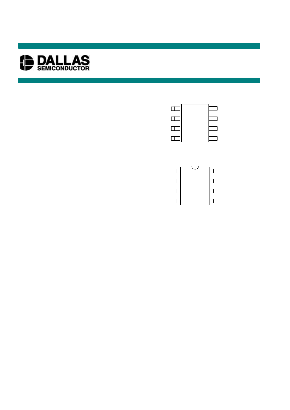
PIN ASSIGNMENT
PIN DESCRIPTION
SDA - 2-Wire Serial Data Input/Output
SCL - 2-Wire Serial Clock
GND - Ground
T
OUT
- Thermostat Output Signal
A0 - Chip Address Input
A1 - Chip Address Input
A2 - Chip Address Input
V
DD
- Power Supply Voltage
DESCRIPTION
The DS1621 Digital Thermometer and Thermostat provides 9–bit temperature readings which indicate
the temperature of the device. The thermal alarm output, T
OUT
, is active when the temperature of the
device exceeds a user–defined temperature TH. The output remains active until the temperature drops
below user defined temperature TL, allowing for any hysteresis necessary.
User-defined temperature settings are stored in nonvolatile memory so parts may be programmed prior to
insertion in a system. Temperature settings and temperature readings are all communicated to/from the
DS1621 over a simple two–wire serial interface.
DS1621
Digital Thermometer and Thermostat
www.dalsemi.com
6
312
475
SDA
T
OUT
GND
VDDA
0
A
1
A2DS1621S 8-PIN SOIC (150-MIL)
DS1621V 8-PIN SOIC (208-MIL)
See Mech Drawings Section
6
312
475
SDA
SCL
T
GND
VDDA
0
A
1
A2DS1621 8-PIN DIP (300-MIL)
See Mech Drawings Section
SCL
Page 2

DS1621
2 of 16 102299
DETAILED PIN DESCRIPTION Table 1
PIN SYMBOL DESCRIPTION
1 SDA Data input/output pin for 2-wire serial communication port.
2 SCL Clock input/output pin for 2-wire serial communication port.
3 T
OUT
Thermostat output. Active when temperature exceeds TH; will reset when
temperature falls below TL.
4 GND Ground pin.
5 A2 Address input pin.
6 A1 Address input pin.
7 A0 Address input pin.
8 V
DD
Supply voltage input power pin. (2.7V – 5.5V)
OPERATION
Measuring Temperature
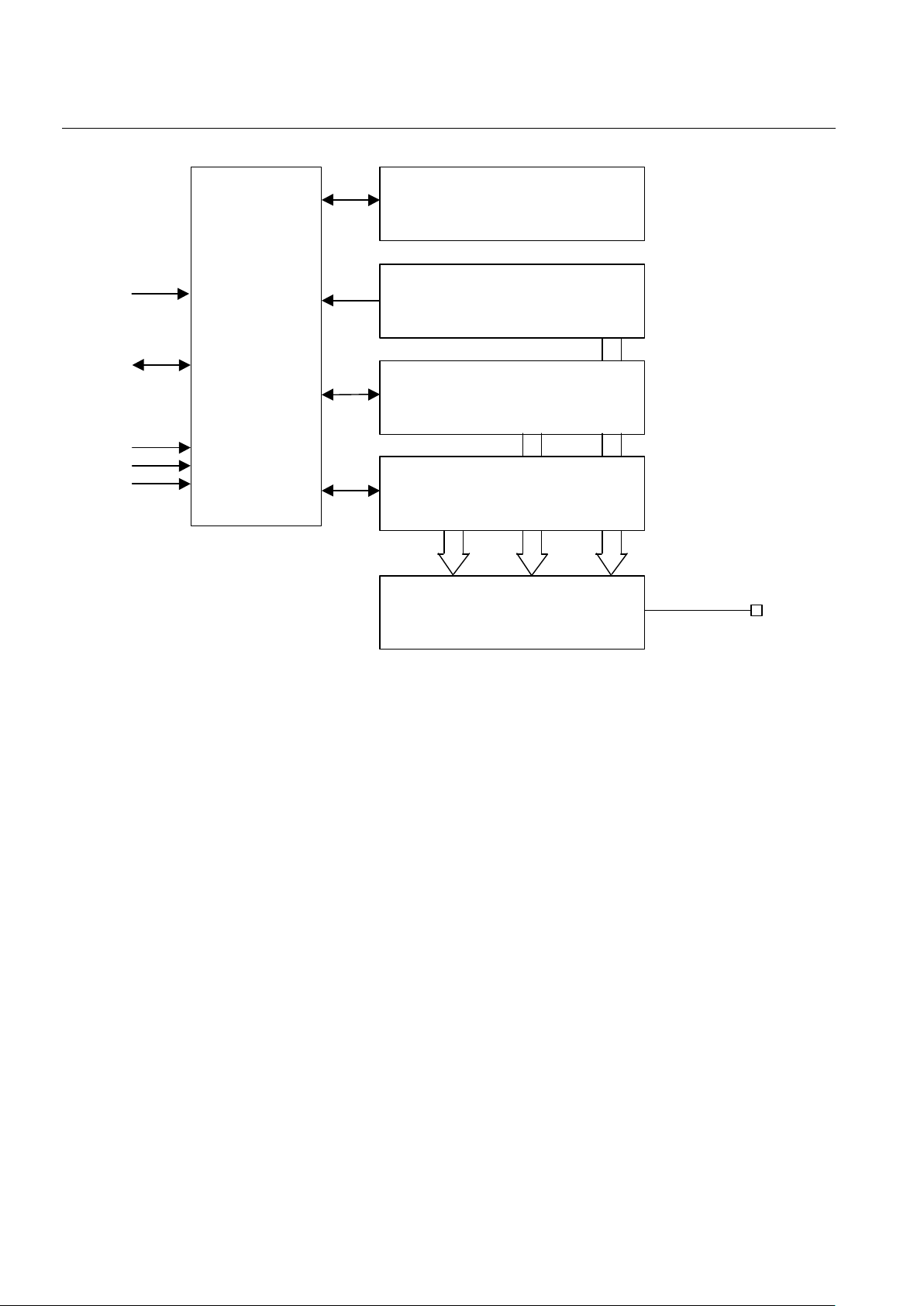
A block diagram of the DS1621 is shown in Figure 1. The DS1621 measures temperatures through the
use of an onboard proprietary temperature measurement technique. A block diagram of the temperature
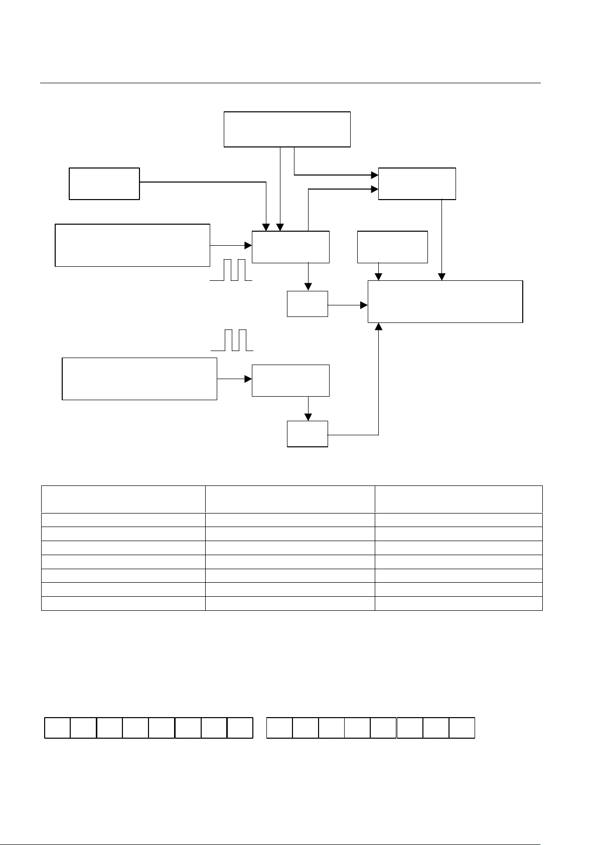
measurement circuitry is shown in Figure 2.
The DS1621 measures temperature by counting the number of clock cycles that an oscillator with a low
temperature coefficient goes through during a gate period determined by a high temperature coefficient
oscillator. The counter is preset with a base count that corresponds to –55°C. If the counter reaches 0
before the gate period is over the temperature register, which is also preset to the –55°C value, is
incremented indicating that the temperature is higher than –55°C.
At the same time, the counter is preset with a value determined by the slope accumulator circuitry. This
circuitry is needed to compensate for the parabolic behavior of the oscillators over temperature. The
counter is then clocked again until it reaches 0. If the gate period is still not finished, then this process
repeats.
The slope accumulator is used to compensate for the nonlinear behavior of the oscillators over
temperature, yielding a high resolution temperature measurement. This is done by changing the number
of counts necessary for the counter to go through for each incremental degree in temperature. To obtain
the desired resolution, both the value of the counter and the number of counts per °C (the value of the
slope accumulator) at a given temperature must be known.
This calculation is done inside the DS1621 to provide 0.5°C resolution. The temperature reading is
provided in a 9–bit, two’s complement reading by issuing the READ TEMPERATURE command. Table
2 describes the exact relationship of output data to measured temperature. The data is transmitted through
the 2–wire serial interface, MSB first. The DS1621 can measure temperature over the range of –55°C to
+125°C in 0.5°C increments. For Fahrenheit usage a lookup table or conversion factor must be used.
Page 3
DS1621
3 of 16 102299
DS1621 FUNCTIONAL BLOCK DIAGRAM Figure 1
STATUS REGISTER &
CONTROL LOGIC
TEMPERATURE SENSOR
HIGH TEMP TRIGGER, TH
LOW TEMP TRIGGER, TL
DIGITAL COMPARATOR/LOGIC
ADDRESS
AND
I/O CONTROL
SCL
SDAA0A1
A2
T
OUT
Page 4
DS1621
4 of 16 102299
TEMPERATURE MEASURING CIRCUITRY Figure 2
TEMPERATURE/DATA RELATIONSHIPS Table 2
TEMPERATURE DIGITAL OUTPUT
(Binary)
DIGITAL OUTPUT
(Hex)
+125°C 01111101 00000000 7B00h
+25°C 00011001 00000000 1900h
+½°C 00000001 00000000 0080h
+0°C 00000000 00000000 0000h
-½°C 11111111 10000000 FF80h
-25°C 11100111 00000000 E700h
-55°C 11001001 00000000 C900h
Since data is transmitted over the 2–wire bus MSB first, temperature data may be written to/read from the
DS1621 as either a single byte (with temperature resolution of 1°C) or as two bytes. The second byte
would contain the value of the least significant (0.5°C) bit of the temperature reading as shown in Table
1. Note that the remaining 7 bits of this byte are set to all "0"s.
Temperature is represented in the DS1621 in terms of a ½°C LSB, yielding the following 9–bit format:
T = -25°C
SLOPE ACCUMULATOR
PRESET COMPARE
LOW TEMPERATURE
COEFFICIENT OSCILLATOR
COUNTER PRESET
=0
TEMPERATURE REGISTER
HIGH TEMPERATURE
COEFFICIENT OSCILLATOR
COUNTER
=0
INC
STOP
SET/CLEAR
LSB
1
1 1 0 0
1
1 1
0
0 0 0 0
0
0 0
MSB
LSB
Page 5
DS1621
5 of 16 102299
Higher resolutions may be obtained by reading the temperature and truncating the 0.5°C bit (the LSB)
from the read value. This value is TEMP_READ. The value left in the counter may then be read by
issuing a READ COUNTER command. This value is the count remaining (COUNT_REMAIN) after the
gate period has ceased. By loading the value of the slope accumulator into the count register (using the
READ SLOPE command), this value may then be read, yielding the number of counts per degree C
(COUNT_PER_C) at that temperature. The actual temperature may be then be calculated by the user
using the following:
TEMPERATURE=TEMP_READ-0.25 +
CPERCOUNT
REMAINCOUNTCPERCOUNT
__
)___(
−
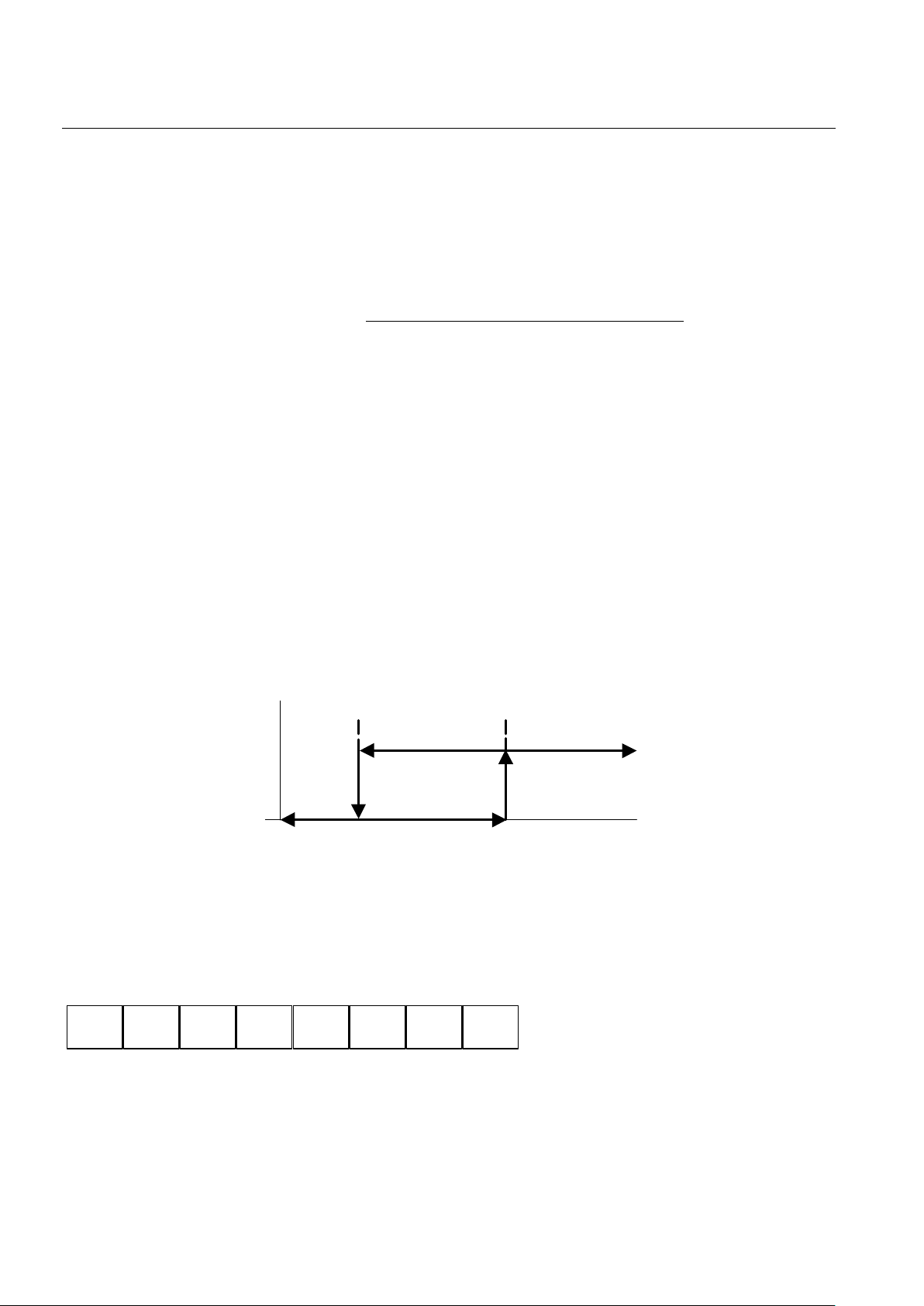
Thermostat Control
In its operating mode, the DS1621 functions as a thermostat with programmable hysteresis as shown in
Figure 3. The thermostat output updates as soon as a temperature conversion is complete.
When the DS1621’s temperature meets or exceeds the value stored in the high temperature trip register
(TH), the output becomes active and will stay active until the temperature falls below the temperature
stored in the low temperature trigger register (TL). In this way, any amount of hysteresis may be
obtained.
The active state for the output is programmable by the user so that an active state may either be a logic
"1" (VDD) or a logic "0" (0V).
THERMOSTAT OUTPUT OPERATION Figure 3
DQ (Thermostat output, Active=High)
OPERATION AND CONTROL
The DS1621 must have temperature settings resident in the TH and TL registers for thermostatic
operation. A configuration/status register also determines the method of operation that the DS1621 will
use in a particular application, as well as indicating the status of the temperature conversion operation.
The configuration register is defined as follows:
where
DONE = Conversion Done bit. “1” = Conversion complete, “0” = Conversion in progress.
TLTHT (°C)
DONE
THF
TLF
NVB
10POL
1SHOT
Page 6

DS1621
6 of 16 102299
THF = Temperature High Flag. This bit will be set to “1” when the temperature is greater than or
equal to the value of TH. It will remain “1” until reset by writing “0” into this location or removing power
from the device. This feature provides a method of determining if the DS1621 has ever been subjected to
temperatures above TH while power has been applied.
TLF = Temperature Low Flag. This bit will be set to “1” when the temperature is less than or equal
to the value of TL. It will remain “1” until reset by writing “0” into this location or removing power from
the device. This feature provides a method of determining if the DS1621 has ever been subjected to
temperatures below TL while power has been applied.
NVB = Nonvolatile Memory Busy flag. “1” = Write to an E
2
memory cell in progress, “0” =
nonvolatile memory is not busy. A copy to E
2
may take up to 10 ms.
POL = Output Polarity Bit. “1” = active high, “0” = active low. This bit is nonvolatile.
1SHOT = One Shot Mode. If 1SHOT is “1”, the DS1621 will perform one temperature conversion upon
receipt of the Start Convert T protocol. If 1SHOT is “0”, the DS1621 will continuously perform
temperature conversions. This bit is nonvolatile.
For typical thermostat operation the DS1621 will operate in continuous mode. However, for applications
where only one reading is needed at certain times or to conserve power, the one–shot mode may be used.
Note that the thermostat output (T
OUT
) will remain in the state it was in after the last valid temperature
conversion cycle when operating in one–shot mode.
2–WIRE SERIAL DATA BUS
The DS1621 supports a bidirectional 2–wire bus and data transmission protocol. A device that sends data
onto the bus is defined as a transmitter, and a device receiving data as a receiver. The device that controls
the message is called a “master." The devices that are controlled by the master are “slaves." The bus must
be controlled by a master device which generates the serial clock (SCL), controls the bus access, and
generates the START and STOP conditions. The DS1621 operates as a slave on the 2–wire bus.
Connections to the bus are made via the open–drain I/O lines SDA and SCL.
The following bus protocol has been defined (See Figure 4):
• Data transfer may be initiated only when the bus is not busy.
• During data transfer, the data line must remain stable whenever the clock line is HIGH. Changes in
the data line while the clock line is high will be interpreted as control signals.
Accordingly, the following bus conditions have been defined:
Bus not busy: Both data and clock lines remain HIGH.
Start data transfer: A change in the state of the data line, from HIGH to LOW, while the clock is HIGH,
defines a START condition.
Stop data transfer: A change in the state of the data line, from LOW to HIGH, while the clock line is
HIGH, defines the STOP condition.
Page 7

DS1621
7 of 16 102299
Data valid: The state of the data line represents valid data when, after a START condition, the data line
is stable for the duration of the HIGH period of the clock signal. The data on the line must be changed
during the LOW period of the clock signal. There is one clock pulse per bit of data.
Each data transfer is initiated with a START condition and terminated with a STOP condition. The
number of data bytes transferred between START and STOP conditions is not limited and is determined
by the master device. The information is transferred byte–wise and each receiver acknowledges with a
ninth–bit.
Within the bus specifications a regular mode (100 kHz clock rate) and a fast mode (400 kHz clock rate)
are defined. The DS1621 works in both modes.
Acknowledge: Each receiving device, when addressed, is obliged to generate an acknowledge after the
reception of each byte. The master device must generate an extra clock pulse which is associated with this
acknowledge bit.
A device that acknowledges must pull down the SDA line during the acknowledge clock pulse in such a
way that the SDA line is stable LOW during the HIGH period of the acknowledge related clock pulse. Of
course, setup and hold times must be taken into account. A master must signal an end of data to the slave
by not generating an acknowledge bit on the last byte that has been clocked out of the slave. In this case,
the slave must leave the data line HIGH to enable the master to generate the STOP condition.
DATA TRANSFER ON 2–WIRE SERIAL BUS Figure 4
Figure 4 details how data transfer is accomplished on the 2–wire bus. Depending upon the state of the
R/W bit, two types of data transfer are possible:
1. Data transfer from a master transmitter to a slave receiver. The first byte transmitted by the
master is the slave address. Next follows a number of data bytes. The slave returns an acknowledge
bit after each received byte.
2. Data transfer from a slave transmitter to a master receiver. The first byte, the slave address,
is transmitted by the master. The slave then returns an acknowledge bit. Next follows a number of
data bytes transmitted by the slave to the master. The master returns an acknowledge bit after all
received bytes other than the last byte. At the end of the last received byte, a ‘not acknowledge’ is
returned.
Page 8

DS1621
8 of 16 102299
The master device generates all of the serial clock pulses and the START and STOP conditions. A
transfer is ended with a STOP condition or with a repeated START condition. Since a repeated START
condition is also the beginning of the next serial transfer, the bus will not be released.
The DS1621 may operate in the following two modes:
1. Slave receiver mode: Serial data and clock are received through SDA and SCL. After each byte is
received an acknowledge bit is transmitted. START and STOP conditions are recognized as the
beginning and end of a serial transfer. Address recognition is performed by hardware after reception
of the slave address and direction bit.
2. Slave transmitter mode: The first byte is received and handled as in the slave receiver mode.
However, in this mode the direction bit will indicate that the transfer direction is reversed. Serial data
is transmitted on SDA by the DS1621 while the serial clock is input on SCL. START and STOP
conditions are recognized as the beginning and end of a serial transfer.
SLAVE ADDRESS
A control byte is the first byte received following the START condition from the master device. The
control byte consists of a 4-bit control code; for the DS1621, this is set as 1001 binary for read and write
operations. The next 3 bits of the control byte are the device select bits (A2, A1, A0). They are used by
the master device to select which of eight devices are to be accessed. These bits are in effect the 3 least
significant bits of the slave address. The last bit of the control byte (R/W) defines the operation to be
performed. When set to a “1” a read operation is selected, when set to a “0” a write operation is selected.
Following the START condition the DS1621 monitors the SDA bus checking the device type identifier
being transmitted. Upon receiving the 1001 code and appropriate device select bits, the slave device
outputs an acknowledge signal on the SDA line.
Page 9

DS1621
9 of 16 102299
2-WIRE SERIAL COMMUNICATION WITH DS1621 Figure 5
Page 10

DS1621
10 of 16 102299
COMMAND SET
Data and control information is read from and written to the DS1621 in the format shown in Figure 5. To
write to the DS1621, the master will issue the slave address of the DS1621 and the R/W bit will be set to
“0”. After receiving an acknowledge, the bus master provides a command protocol. After receiving this
protocol, the DS1621 will issue an acknowledge and then the master may send data to the DS1621. If the
DS1621 is to be read, the master must send the command protocol as before and then issue a repeated
START condition and the control byte again, this time with the R/W bit set to “1” to allow reading of the
data from the DS1621. The command set for the DS1621 as shown in Table 3 is as follows:
Read Temperature [AAh]
This command reads the last temperature conversion result. The DS1621 will send 2 bytes, in the format
described earlier, which are the contents of this register.
Access TH [A1h]
If R/W is “0” this command writes to the TH (HIGH TEMPERATURE) register. After issuing this
command, the next 2 bytes written to the DS1621, in the same format as described for reading
temperature, will set the high temperature threshold for operation of the T
OUT
output. If R/
W
is “1” the
value stored in this register is read back.
Access TL [A2h]
If R/W is “0” this command writes to the TL (LOW TEMPERATURE) register. After issuing this
command, the next 2 bytes written to the DS1621, in the same format as described for reading
temperature, will set the high temperature threshold for operation of the T
OUT
output. If R/
W
is “1” the
value stored in this register is read back.
Access Config [ACh]
If R/W is “0” this command writes to the configuration register. After issuing this command, the next
data byte is the value to be written into the configuration register. If R/W is “1” the next data byte read is
the value stored in the configuration register.
Read Counter [A8h]
This command reads the value of the counter byte. This command is valid only if R/W is “1”.
Read Slope [A9h]
This command reads the value of the slope counter byte from the DS1621. This command is valid only if
R/W is “1”.
Start Convert T [EEh]
This command begins a temperature conversion. No further data is required. In one–shot mode the
temperature conversion will be performed and then the DS1621 will remain idle. In continuous mode this
command will initiate continuous conversions.
Stop Convert T [22h]
This command stops temperature conversion. No further data is required. This command may be used to
halt a DS1621 in continuous conversion mode. After issuing this command, the current temperature
Page 11

DS1621
11 of 16 102299
measurement will be completed and the DS1621 will remain idle until a Start Convert T is issued to
resume continuous operation.
DS1621 COMMAND SET Table 3
INSTRUCTION DESCRIPTION PROTOCOL
2-WIRE BUS DATA
AFTER ISSUING
PROTOCOL NOTES
TEMPERATURE CONVERSION COMMANDS
Read Temperature Read last converted temperature
value from temperature register.
AAh <read 2 bytes data>
Read Counter Reads value of count remaining
from counter.
A8h <read data>
Read Slope Reads value of the slope
accumulator.
A9h <read data>
Start Convert T Initiates temperature
conversion.
EEh idle 1
Stop Convert T Halts temperature conversion. 22h idle 1
THERMOSTAT COMMANDS
Access TH Reads or writes high
temperature limit value into TH
register.
A1h <write data> 2
Access TL Reads or writes low
temperature limit value into TL
register.
A2h <write data> 2
Access Config Reads or writes configuration
data to configuration register.
ACh <write data> 2
NOTES:
1. In continuous conversion mode a Stop Convert T command will halt continuous conversion. To
restart the Start Convert T command must be issued. In one–shot mode a Start Convert T command
must be issued for every temperature reading desired.
2. Writing to the E
2
typically requires 10ms at room temperature. After issuing a write command, no
further writes should be requested for at least 10 ms.
Page 12

DS1621
12 of 16 102299
MEMORY FUNCTION EXAMPLE
Example: Bus master sets up DS1621 for continuous conversion and thermostatic function.
BUS MASTER
MODE
DS1621
MODE
DATA (MSB
FIRST) COMMENTS
TX RX START Bus Master initiates a START condition.
TX RX <address,0>
Bus Master sends DS1621 address; R/W = 0.
RX TX ACK DS1621 generates acknowledge bit.
TX RX ACh Bus Master sends Access Config command protocol.
RX TX ACK DS1621 generates acknowledge bit.
TX RX 02h Bus Master sets up DS1621 for output polarity active
high, continuous conversion.
RX TX ACK DS1621 generates acknowledge bit.
TX RX START Bus Master generates a repeated START condition.
TX RX <address,0>
Bus Master sends DS1621 address; R/W = 0.
RX TX ACK DS1621 generates acknowledge bit.
TX RX A1h Bus Master sends Access TH command.
RX TX ACK DS1621 generates acknowledge bit.
TX RX 28h Bus Master sends first byte of data for TH limit of
+40°C.
RX TX ACK DS1621 generates acknowledge bit.
TX RX 00h Bus Master sends second byte of data for TH limit of
+40°C.
RX TX ACK DS1621 generates acknowledge bit.
TX RX START Bus Master generates a repeated START condition.
TX RX <address,0>
Bus Master sends DS1621 address; R/W = 0.
RX TX ACK DS1621 generates acknowledge bit.
TX RX A2h Bus Master sends Access TL command.
RX TX ACK DS1621 generates acknowledge bit.
TX RX 0Ah Bus Master sends first byte of data for TL limit of
+10°C.
RX TX ACK DS1621 generates acknowledge bit.
TX RX 00h Bus Master sends second byte of data for TL limit of
+10°C.
RX TX ACK DS1621 generates acknowledge bit.
TX RX START Bus Master generates a repeated START condition.
TX RX <address,0>
Bus Master sends DS1621 address; R/W = 0.
RX TX ACK DS1621 generates acknowledge bit.
TX RX EEh Bus Master sends Start Convert T command protocol.
RX TX ACK DS1621 generates acknowledge bit.
TX RX STOP Bus Master initiates STOP condition.
Page 13

DS1621
13 of 16 102299
ABSOLUTE MAXIMUM RATINGS*
Voltage on Any Pin Relative to Ground –0.5V to +7.0V
Operating Temperature –55°C to +125°C
Storage Temperature –55°C to +125°C
Soldering Temperature 260°C for 10 seconds
* This is a stress rating only and functional operation of the device at these or any other conditions above
those indicated in the operation sections of this specification is not implied. Exposure to absolute
maximum rating conditions for extended periods of time may affect reliability.
RECOMMENDED DC OPERATING CONDITIONS
PARAMETER SYMBOL MIN TYP MAX UNITS NOTES
Supply Voltage V
DD
2.7 5.5 V 1
DC ELECTRICAL CHARACTERISTICS (-55°C to +125°C; VDD=2.7V to 5.5V)
PARAMETER SYMBOL CONDITION MIN TYP MAX UNITS NOTES
±½ °CThermometer Error T
ERR
0°C to 70°C
-55°C to + 0°C
and
70°C to 125°C
See Typical Curve
11
Low Level Input
Voltage
V
IL
0.5 0.3 V
DD
V
High Level Input
Voltage
V
IH
0.7 V
DD
VDD+0.5 V
Pulse width of
spikes which must
be suppressed by
the input filter
t
SP
Fast Mode 0 50 ns
V
OL1
3 mA Sink
Current
0 0.4 VLow Level Output
Voltage
V
OL2
6 mA Sink
Current
0 0.6 V
Input Current each
I/O Pin
0.4<V
I/O
<0.9V
DD
-10 10 µA 2
I/O Capacitance C
I/O
10 pF
Active Supply
Current
I
CC
Temperature
Conversion
E2 Write
Communi-
cation Only
1000
400
100
µA 3, 4
Standby Supply
Current
I
STBY
1 µA 3, 4
V
OH
1 mA Source 2.4 VThermostat Output
(T
OUT
) Output
Voltage
V
OL
4 mA Sink 0.4 V
Page 14

DS1621
14 of 16 102299
AC ELECTRICAL CHARACTERISTICS (-55°C to +125°C; VDD=2.7V to 5.5V)
PARAMETER SYMBOL CONDITION MIN TYP MAX UNITS NOTES
Temperature
Conversion Time
T
TC
0.4 1 s
NV Write Cycle
Time
t
WR
0°C to 70°C 10 50 ms 10
SCL Clock
Frequency
f
SCL
Fast Mode
Standard Mode
0
0
400
100
KHz
Bus Free Time
Between a STOP
and START
Condition
t
BUF
Fast Mode
Standard Mode
1.3
4.7
µs
Hold Time
(Repeated) START
Condition
t
HD:STA
Fast Mode
Standard Mode
0.6
4.0
µs 5
Low Period of SCL
Clock
T
LOW
Fast Mode
Standard Mode
1.3
4.7
µs
High Period of SCL
Clock
T
HIGH
Fast Mode
Standard Mode
0.6
4.0
µs
Setup Time for a
Repeated START
Condition
t
SU:STA
Fast Mode
Standard Mode
0.6
4.7
µs
Data Hold Time t
HD:DAT
Fast Mode
Standard Mode
0
0
0.9 µs 6, 7
Data Setup Time t
SU:DAT
Fast Mode
Standard Mode
100
250
ns 8
Rise Time of Both
SDA and SCL
Signals
t
R
Fast Mode
Standard Mode
20+0.1C
B
300
1000
ns 9
Fall Time of both
SDA and SCL
Signals
t
F
Fast Mode
Standard Mode
20+0.1C
B
300
300
ns 9
Setup time for
STOP Condition
t
SU:STO
Fast Mode
Standard Mode
0.6
4.0
µs
Capacitative Load
for each Bus Line
C
b
400 pF
All values referred to VIH=0.9 VDD and VIL=0.1 VDD.
AC ELECTRICAL CHARACTERISTICS (-55°C to +125°C; VDD=2.7V to 5.5V)
PARAMETER SYMBOL MIN TYP MAX UNITS NOTES
Input Capacitance C
I
5 pF
Page 15

DS1621
15 of 16 102299
NOTES:
1. All voltages are referenced to ground.
2. I/O pins of fast mode devices must not obstruct the SDA and SCL lines if V
DD
is switched off.
3. I
CC
specified with T
OUT
pin open.
4. ICC specified with VCC at 5.0V and SDA, SCL = 5.0V, 0°C to 70°C.
5. After this period, the first clock pulse is generated.
6. A device must internally provide a hold time of at least 300 ns for the SDA signal (referred to the
V
IH MIN
of the SCL signal) in order to bridge the undefined region of the falling edge of SCL.
7. The maximum t
HD:DAT
has only to be met if the device does not stretch the LOW period (t
LOW
) of the
SCL signal.
8. A fast mode device can be used in a standard mode system, but the requirement t
SU:DAT
>250 ns must
then be met. This will automatically be the case if the device does not stretch the LOW period of the
SCL signal. If such a device does stretch the LOW period of the SCL signal, it must output the next
data bit to the SDA line t
RMAX+tSU:DAT
= 1000+250 = 1250 ns before the SCL line is released.
9. C
b
– total capacitance of one bus line in pF.
10. Writing to the nonvolatile memory should only take place in the 0°C to 70°C temperature range.
11. See typical curve for specification limits outside 0°C to 70°C range. Thermometer error reflects
sensor accuracy as tested during calibration.
TIMING DIAGRAM
Page 16

DS1621
16 of 16 102299
TYPICAL PERFORMANCE CURVE
DS1621 DIGITAL THERMOMETER AND THERMOSTAT
TEMPERATURE READING ERROR
TEMPERATURE (deg. C)
 Loading...