

Page 1

General Description
The DS12885, DS12887, and DS12C887 real-time
clocks (RTCs) are designed to be direct replacements
for the DS1285 and DS1287. The devices provide a
real-time clock/calendar, one time-of-day alarm, three
maskable interrupts with a common interrupt output, a
programmable square wave, and 114 bytes of batterybacked static RAM (113 bytes in the DS12C887 and
DS12C887A). The DS12887 integrates a quartz crystal
and lithium energy source into a 24-pin encapsulated
DIP package. The DS12C887 adds a century byte at
address 32h. For all devices, the date at the end of the
month is automatically adjusted for months with fewer
than 31 days, including correction for leap years. The
devices also operate in either 24-hour or
12-hour format with an AM/PM indicator. A precision
temperature-compensated circuit monitors the status of
VCC. If a primary power failure is detected, the device
automatically switches to a backup supply. A lithium
coin-cell battery can be connected to the V
BAT
input
pin on the DS12885 to maintain time and date operation
when primary power is absent. The device is accessed
through a multiplexed byte-wide interface, which supports both Intel and Motorola modes.
Applications
Embedded Systems
Utility Meters
Security Systems
Network Hubs, Bridges, and Routers
Features
♦ Drop-In Replacement for IBM AT Computer
Clock/Calendar
♦ RTC Counts Seconds, Minutes, Hours, Day, Date,
Month, and Year with Leap Year Compensation
Through 2099
♦ Binary or BCD Time Representation
♦ 12-Hour or 24-Hour Clock with AM and PM in
12-Hour Mode
♦ Daylight Saving Time Option
♦ Selectable Intel or Motorola Bus Timing
♦ Interfaced with Software as 128 RAM Locations
♦ 14 Bytes of Clock and Control Registers
♦ 114 Bytes of General-Purpose, Battery-Backed
RAM (113 Bytes in the DS12C887 and
DS12C887A)
♦ RAM Clear Function (DS12885, DS12887A, and
DS12C887A)
♦ Interrupt Output with Three Independently
Maskable Interrupt Flags
♦ Time-of-Day Alarm Once Per Second to Once
Per Day
♦ Periodic Rates from 122µs to 500ms
♦ End-of-Clock Update Cycle Flag
♦ Programmable Square-Wave Output
♦ Automatic Power-Fail Detect and Switch Circuitry
♦ Optional 28-Pin PLCC Surface Mount Package or
32-Pin TQFP (DS12885)
♦ Optional Encapsulated DIP (EDIP) Package with
Integrated Crystal and Battery (DS12887,
DS12887A, DS12C887, DS12C887A)
♦ Optional Industrial Temperature Range Available
♦ Underwriters Laboratory (UL) Recognized
DS12885/DS12887/DS12887A/DS12C887/DS12C887A
Real-Time Clock
______________________________________________ Maxim Integrated Products 1
DS12885
DS83C520
R/W
AS
GND
X2X1
V
CC
V
CC
CRYSTAL
DS
V
BAT
AD(0–7) SQW
RESET
IRQ
RCLR
CS
MOT
Typical Operating Circuit
Rev 2; 5/06
For pricing, delivery, and ordering information, please contact Maxim/Dallas Direct! at
1-888-629-4642, or visit Maxim’s website at www.maxim-ic.com.
Pin Configurations and Ordering Information appear at end of data sheet.
Page 2

DS12885/DS12887/DS12887A/DS12C887/DS12C887A
Real-Time Clock
2 _____________________________________________________________________
ABSOLUTE MAXIMUM RATINGS
Stresses beyond those listed under “Absolute Maximum Ratings” may cause permanent damage to the device. These are stress ratings only, and functional
operation of the device at these or any other conditions beyond those indicated in the operational sections of the specifications is not implied. Exposure to
absolute maximum rating conditions for extended periods may affect device reliability.
Voltage Range on VCCPin Relative to Ground .....-0.3V to +6.0V
Operating Temperature Range ...................................................
Commercial (noncondensing) .............................0°C to +70°C
Operating Temperature Range ...................................................
Industrial (noncondensing)...............................-40°C to +85°C
Storage Temperature Range .............................-55°C to +125°C
Soldering Temperature .......................................See IPC/JEDEC
J-STD-020 Specification (Note 1)
Soldering Temperature (leads, 10s) ................................+260°C
DC ELECTRICAL CHARACTERISTICS
(V
CC
= +4.5V to +5.5V, TA= over the operating range, unless otherwise noted.) (Note 2)
PARAMETER
CONDITIONS
UNITS
Supply Voltage V
CC
(Note 3) 4.5 5.5 V
V
BAT
Input Voltage V
BAT
(Note 3) 2.5 4.0 V
Input Logic 1 V
IH
(Note 3) 2.2
V
CC
+
0.3
V
Input Logic 0 V
IL
(Note 3)
V
VCC Power-Supply Current I
CC1
(Note 4) 15 mA
VCC Standby Current I
CCS
(Note 5) mA
Input Leakage I
IL
µA
I/O Leakage I
OL
(Note 6)
µA
Input Current I
MOT
(Note 7)
µA
Output at 2.4V I
OH
(Note 3)
mA
Output at 0.4V I
OL
(Note 3) 4.0 mA
Power-Fail Voltage V
PF
(Note 3) 4.0
4.5 V
VRT Trip Point
1.3 V
SYMBOL
MIN TYP MAX
-0.3 +0.8
-1.0 +1.0
-1.0 +1.0
-1.0 +500
-1.0
4.25
VRT
TRIP
Page 3
DS12885/DS12887/DS12887A/DS12C887/DS12C887A
Real-Time Clock
_____________________________________________________________________ 3
DC ELECTRICAL CHARACTERISTICS
(VCC= 0V, V
BAT
= 3.0V, TA= over the operating range, unless otherwise noted.) (Note 2)
PARAMETER
CONDITIONS
UNITS
V
BAT
Current (OSC On);
T
A
= +25°C, V
BACKUP
= 3.0V
I
BAT
(Note 8) 500 nA
V
BAT
Current (Oscillator Off) I
BATDR
(Note 8) 100 nA
AC ELECTRICAL CHARACTERISTICS
(VCC= 4.5V to 5.5V, TA= over the operating range.) (Note 2)
PARAMETER
CONDITIONS
Cycle Time t
CYC
DC ns
Pulse Width, DS Low or R/W High
PW
EL
ns
Pulse Width, DS High or R/W Low
PW
EH
ns
Input Rise and Fall tR, t
F
30 ns
R/W Hold Time t
RWH
10 ns
R/W Setup Time Before DS/E t
RWS
50 ns
Chip-Select Setup Time Before
DS or R/W
t
CS
20 ns
Chip-Select Hold Time t
CH
0ns
Read-Data Hold Time t
DHR
10 80 ns
Write-Data Hold Time t
DHW
0ns
Address Valid Time to AS Fall t
ASL
30 ns
Address Hold Time to AS Fall t
AHL
10 ns
Delay Time DS/E to AS Rise t
ASD
20 ns
Pulse Width AS High PW
ASH
60 ns
Delay Time, AS to DS/E Rise t
ASED
40 ns
Output Data Delay Time from DS
or R/W
t
DDR
20 120 ns
Data Setup Time t
DSW
ns
Reset Pulse Width t
RWL
5µs
IRQ Release from DS t
IRDS
2µs
IRQ Release from RESET t
IRR
2µs
SYMBOL
SYMBOL
MIN TYP MAX
MIN TYP MAX UNITS
385
150
125
100
Page 4
DS12885/DS12887/DS12887A/DS12C887/DS12C887A
Real-Time Clock
4 _____________________________________________________________________
PW
ASH
PW
EL
t
ASED
t
CYC
t
RWS
t
CS
t
RWH
t
CH
PW
EH
t
ASD
AD0–AD7
READ
CS
R/ W
AS
DS
AD0–AD7
WRITE
t
DHW
t
DHR
t
DDR
t
AHL
t
ASL
t
DSW
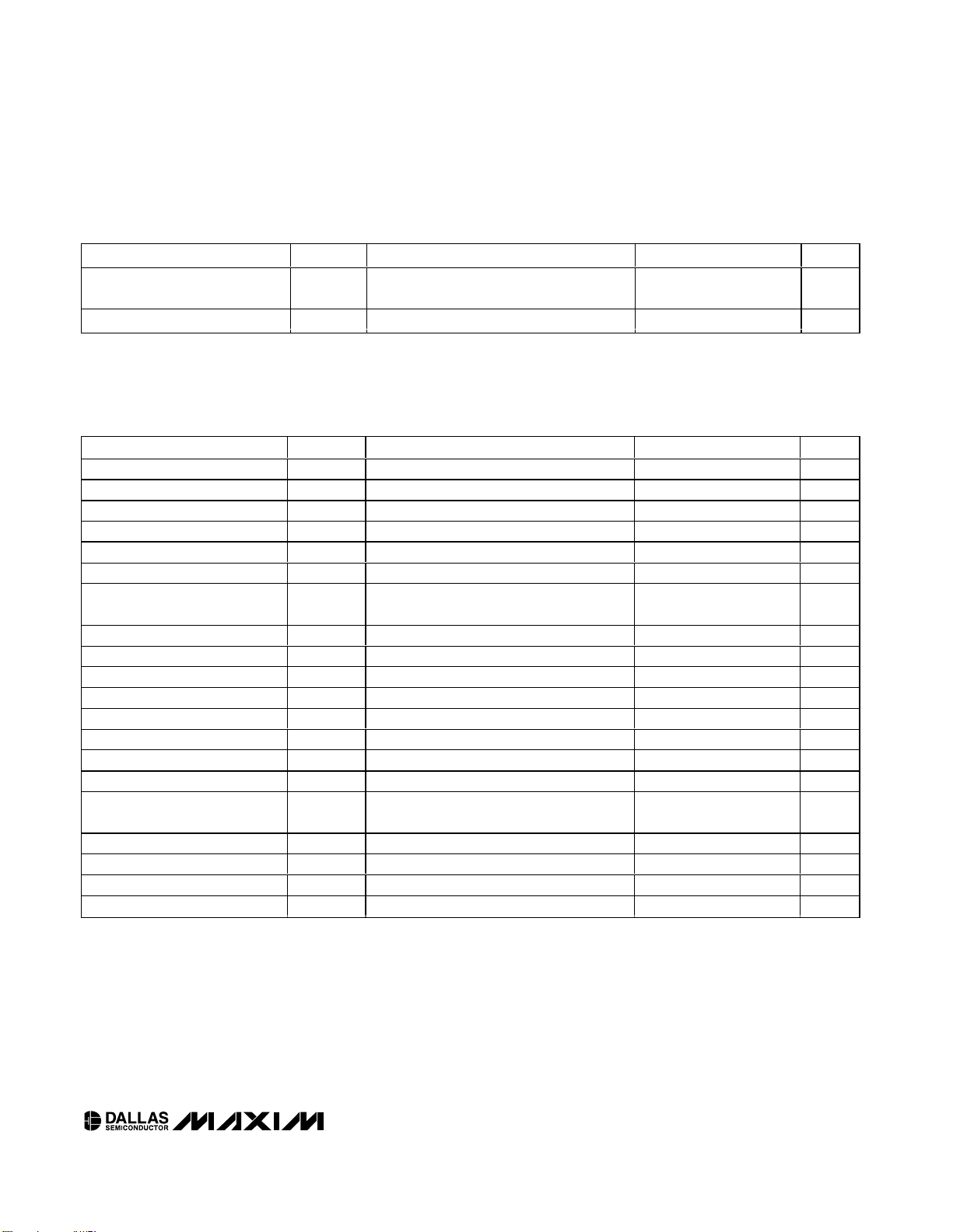
Motorola Bus Read/Write Timing
Intel Bus Write Timing
PW
ASH
PW
EL
PW
EH
t
CS
t
AHL
t
ASL
t
DSW
t
DHW
t
CH
t
ASD
t
ASD
t
CYC
CS
R/W
AS
DS
AD0–AD7
WRITE
t
ASED
Page 5
DS12885/DS12887/DS12887A/DS12C887/DS12C887A
Real-Time Clock
_____________________________________________________________________ 5
t
CS
t
AHL
t
ASL
t
CYC
PW
ASH
PW
ASL
PW
EH
CS
R/W
AS
DS
AD0–AD7
t
ASD
t
ASD
t
ASED
t
DDR
t
DHR
t
CH
Intel Bus Read Timing
t
RWL
t
IRR
t
IRDS
DS
RESET
IRQ
IRQ
Release Delay Timing
OUTPUTS
INPUTS
HIGH-Z
DON'T CARE
VALID
RECOGNIZED
RECOGNIZED
VALID
V
CC
t
F
V
PF(MAX)
V
PF(MIN)
t
RPU
t
R
t
DR
Power-Up/Power-Down Timing
Page 6

DS12885/DS12887/DS12887A/DS12C887/DS12C887A
Real-Time Clock
6 _____________________________________________________________________
POWER-UP/POWER-DOWN CHARACTERISTICS
(TA= -40°C to +85°C) (Note 2)
PARAMETER
CONDITIONS
UNITS
Recovery at Power-Up t
RPU
20 200 ms
VCC Fall Time; V
PF(MAX)
to
V
PF(MIN)
t
F
300 µs
VCC Rise Time; V
PF(MIN)
to
V
PF(MAX)
t
R
0µs
CAPACITANCE
(TA= +25°C) (Note 9)
PARAMETER
CONDITIONS
UNITS
Capacitance on All Input Pins
Except X1 and X2
C
IN
5pF
Capacitance on IRQ, SQW, and
DQ Pins
C
IO
7pF
DATA RETENTION
(TA= +25°C)
PARAMETER
CONDITIONS
UNITS
Expected Data Retention t
DR
10
years
AC TEST CONDITIONS
PARAMETER TEST CONDITIONS
Input Pulse Levels 0 to 3.0V
Output Load Including Scope and Jig 50pF + 1TTL Gate
Input and Output Timing Measurement Reference Levels Input/Output: VIL maximum and VIH minimum
Input-Pulse Rise and Fall Times 5ns
WARNING: Negative undershoots below -0.3V while the part is in battery-backed mode may cause loss of data.
Note 1: RTC modules can be successfully processed through conventional wave-soldering techniques as long as temperature
exposure to the lithium energy source contained within does not exceed +85°C. However, post-solder cleaning with waterwashing techniques is acceptable, provided that ultrasonic vibrations are not used to prevent crystal damage.
Note 2: Limits at -40°C are guaranteed by design and not production tested.
Note 3: All voltages are referenced to ground.
Note 4: All outputs are open.
Note 5: Specified with
CS = DS = R/W = RESET = VCC; MOT, AS, AD0–AD7 = 0; V
BACKUP
open.
Note 6: Applies to the AD0 to AD7 pins, the IRQ pin, and the SQW pin when each is in a high-impedance state.
Note 7: The MOT pin has an internal 20kΩ pulldown.
Note 8: Measured with a 32.768kHz crystal attached to X1 and X2.
Note 9: Guaranteed by design. Not production tested.
Note 10: Measured with a 50pF capacitance load.
SYMBOL
SYMBOL
SYMBOL
MIN TYP MAX
MIN TYP MAX
MIN TYP MAX
Page 7
DS12885/DS12887/DS12887A/DS12C887/DS12C887A
Real-Time Clock
_____________________________________________________________________ 7
Typical Operating Characteristics
(VCC= +5.0V, TA= +25°C, unless otherwise noted.)
OSCILLATOR FREQUENCY
vs. V
CC
DS12885 toc02
VCC (V)
FREQUENCY (Hz)
5.3
5.04.8
32768.10
32768.20
32768.30
32768.40
32768.50
32768.60
32768.70
32768.00
4.5 5.5
I
BAT1
vs. V
BAT
vs. TEMPERATURE
DS12885 toc01
V
BAT
(V)
I
BAT
(nA)
3.82.8
3.0
3.3
3.5
200
300
250
150
2.5
4.0
VCC = 0V
+85°C
+25°C
0°C
-40°C
+70°C
+40°C
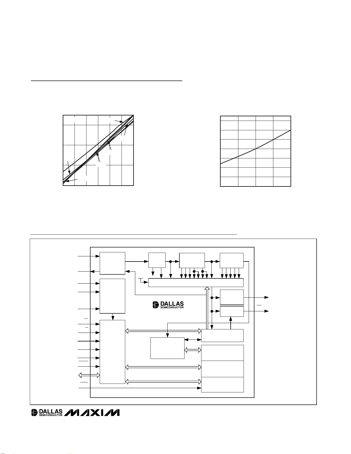
POWER
CONTROL
GND
OSC
BUS
INTERFACE
V
CC
X1
X2
RESET
CS
DS
AS
R/W
MOT
AD0–AD7
DIVIDE
BY 8
DIVIDE
BY 64
DIVIDE
BY 64
16:1 MUX
SQUARE-
WAVE
GENERATOR
REGISTERS A, B, C, D
CLOCK/CALENDAR AND
ALARM REGISTERS
USER RAM
114 BYTES
CLOCK/CALENDAR
UPDATE LOGIC
IRQ
SQW
IRQ
GENERATOR
BUFFERED CLOCK/
CALENDAR AND ALARM
REGISTERS
V
BAT
RLCR
DS12885
Functional Diagram
Page 8

DS12885/DS12887/DS12887A/DS12C887/DS12C887A
Real-Time Clock
8 _____________________________________________________________________
Pin Description
PIN
SO,
PDIP
FUNCTION
11229
Motorola or Intel Bus Timing Selector. This pin selects one of two bus types. When
connected to V
CC
, Motorola bus timing is selected. When connected to GND or
left disconnected, Intel bus timing is selected. The pin has an internal pulldown
resistor.
2—330X1
3—431X2
Connections for Standard 32.768kHz Quartz Crystal. The internal oscillator
circuitry is designed for operation with a crystal having a 6pF specified load
capacitance (C
L
). Pin X1 is the input to the oscillator and can optionally be
connected to an external 32.768kHz oscillator. The output of the internal oscillator,
pin X2, is floated if an external oscillator is connected to pin X1.
4–11
1, 2, 3,
5, 7, 8,
9, 11
Multiplexed, Bidirectional Address/Data Bus. The addresses are presented during
the first portion of the bus cycle and latched into the device by the falling edge of
AS. Write data is latched by the falling edge of DS (Motorola timing) or the rising
edge of R/W (Intel timing). In a read cycle, the device outputs data during the
latter portion of DS (DS and R/W high for Motorola timing, DS low and R/W high for
Intel timing). The read cycle is terminated and the bus returns to a highimpedance state as DS transitions low in the case of Motorola timing or as DS
transitions high in the case of Intel timing.
12, 16
12
Ground
13 13 16 13 CS
Active-Low Chip-Select Input. The chip-select signal must be asserted low for a
bus cycle in the device to be accessed. CS must be kept in the active state during
DS and AS for Motorola timing and during DS and R/W for Intel timing. Bus cycles
that take place without asserting CS will latch addresses, but no access occurs.
When V
CC
is below VPF volts, the device inhibits access by internally disabling the
CS input. This action protects the RTC data and the RAM data during power
outages.
14 14 17 14 AS
Address Strobe Input. A positive-going address-strobe pulse serves to
demultiplex the bus. The falling edge of AS causes the address to be latched
within the device. The next rising edge that occurs on the AS bus clears the
address regardless of whether CS is asserted. An address strobe must
immediately precede each write or read access. If a write or read is performed
with CS deasserted, another address strobe must be performed prior to a read or
write access with CS asserted.
15 15 19 16
Read/Write Input. The R/W pin has two modes of operation. When the MOT pin is
connected to V
CC
for Motorola timing, R/W is at a level that indicates whether the
current cycle is a read or write. A read cycle is indicated with a high level on R/W
while DS is high. A write cycle is indicated when R/W is low during DS. When the
MOT pin is connected to GND for Intel timing, the R/W signal is an active-low
signal. In this mode, the R/W pin operates in a similar fashion as the write-enable
signal (WE) on generic RAMs. Data are latched on the rising edge of the signal.
EDIP PLCC TQFP
4–11
5–10,
12, 14
15, 20 12, 17 GND
NAME
MOT
AD0–
AD7
R/W
Page 9

DS12885/DS12887/DS12887A/DS12C887/DS12C887A
Real-Time Clock
_____________________________________________________________________ 9
Pin Description (continued)
PIN
SO,
PDIP
FUNCTION
22
16, 20,
1, 11,
13, 18,
26
4, 6, 10,
15, 20,
23, 25,
No Connection. This pin should remain unconnected. Pin 21 is RCLR for the
DS12887A/DS12C887A. On the EDIP, these pins are missing by design.
17 17 21 18 DS
D ata S tr ob e or Read Inp ut. The D S p i n has tw o m od es of op er ati on d ep end i ng on
the l evel of the M O T p i n. W hen the M O T p i n i s connected to V
C C
, M otor ol a b us
ti m i ng i s sel ected . In thi s m od e, D S i s a p osi ti ve p ul se d ur i ng the l atter p or ti on of the
b us cycl e and i s cal l ed d ata str ob e. D ur i ng r ead cycl es, D S si g ni fi es the ti m e that the
device i s to d r i ve the b i d i r ecti onal b us. In w r i te cycl es, the tr ai l i ng ed g e of D S causes
the device to l atch the w r i tten d ata. W hen the M O T p i n i s connected to GN D , Intel
b
us ti m i ng i s sel ected . D S i d enti fi es the ti m e p er i od w hen the device d r i ves the b us
w i th r ead d ata. In thi s m od e, the D S p i n op er ates i n a si m i l ar fashi on as the outp utenab l e ( O E ) si g nal on a g ener i c RAM .
18 18 22 19
Active-Low Reset Input. The RESET pin has no effect on the clock, calendar, or
RAM. On power-up, the RESET pin can be held low for a time to allow the power
supply to stabilize. The amount of time that RESET is held low is dependent on the
application. However, if RESET is used on power-up, the time RESET is low should
exceed 200ms to ensure that the internal timer that controls the device on power-
up has timed out. When RESET is low and VCC is above VPF, the following occurs:
A. Periodic interrupt-enable (PIE) bit is cleared to 0.
B. Alarm interrupt-enable (AIE) bit is cleared to 0.
C. Update-ended interrupt-enable (UIE) bit is cleared to 0.
D. Periodic-interrupt flag (PF) bit is cleared to 0.
E. Alarm-interrupt flag (AF) bit is cleared to 0.
F. Update-ended interrupt flag (UF) bit is cleared to 0.
G. Interrupt-request status flag (IRQF) bit is cleared to 0.
H. IRQ pin is in the high-impedance state.
I. The device is not accessible until RESET is returned high.
J. Square-wave output-enable (SQWE) bit is cleared to 0.
In a typical application, RESET can be connected to V
CC
. This connection allows
the device to go in and out of power fail without affecting any of the control
registers.
EDIP PLCC TQFP
2, 3,
21, 22
27, 32
NAME
N.C.
RESET
Page 10

DS12885/DS12887/DS12887A/DS12C887/DS12C887A
Real-Time Clock
10 ____________________________________________________________________
Pin Description (continued)
PIN
SO,
PDIP
EDIP
FUNCTION
19 19 23 21
Active-Low Interrupt Request Output. The IRQ pin is an active-low output of the
device that can be used as an interrupt input to a processor. The IRQ output
remains low as long as the status bit causing the interrupt is present and the
corresponding interrupt-enable bit is set. The processor program normally
reads the C register to clear the IRQ pin. The RESET pin also clears pending
interrupts. When no interrupt conditions are present, the IRQ level is in the highimpedance state. Multiple interrupting devices can be connected to an IRQ
bus, provided that they are all open drain. The IRQ pin is an open-drain output
and requires an external pullup resistor to V
CC
.
20 — 24 22
Connection for a Primary Battery. (DS12885 Only.) Battery voltage must be held
between the minimum and maximum limits for proper operation. If a backup
supply is not supplied, V
BAT
must be grounded. Connect the battery directly to
the V
BAT
pin. Diodes in series between the V
BAT
pin and the battery may
prevent proper operation. UL recognized to ensure against reverse charging
when used with a lithium battery.
21
21
(DS12887A/
25 24
Active-Low RAM Clear. The RCLR pin is used to clear (set to logic 1) all the
general-purpose RAM, but does not affect the RAM associated with the RTC. To
clear the RAM, RCLR must be forced to an input logic 0 during battery-backup
mode when V
CC
is not applied. The RCLR function is designed to be used
through a human interface (shorting to ground manually or by a switch) and not
to be driven with external buffers. This pin is internally pulled up. Do not use an
external pullup resistor on this pin.
23 23 27 26
Square-Wave Output. The SQW pin can output a signal from one of 13 taps
provided by the 15 internal divider stages of the RTC. The frequency of the
SQW pin can be changed by programming Register A, as shown in Table 1.
The SQW signal can be turned on and off using the SQWE bit in Register B. The
SQW signal is not available when V
CC
is less than VPF.
24 24 28 28
DC Power Pin for Primary Power Supply. When VCC is applied within normal
limits, the device is fully accessible and data can be written and read. When
V
CC
is below VPF reads and writes are inhibited.
PLCC TQFP
DS12C887A)
NAME
IRQ
V
BAT
RCLR
SQW
V
CC
Page 11

DS12885/DS12887/DS12887A/DS12C887/DS12C887A
Real-Time Clock
____________________________________________________________________ 11
Detailed Description
The DS12885 family of RTCs provide 14 bytes of realtime clock/calendar, alarm, and control/status registers
and 114 bytes (113 bytes for DS12C887 and
DS12C887A) of nonvolatile, battery-backed static RAM.
A time-of-day alarm, three maskable interrupts with a
common interrupt output, and a programmable squarewave output are available. The devices also operate in
either 24-hour or 12-hour format with an AM/PM indicator. A precision temperature-compensated circuit monitors the status of VCC. If a primary power-supply failure
is detected, the devices automatically switch to a backup supply. The backup supply input supports a primary
battery, such as lithium coin cell. The devices are
accessed through a multiplexed address/data bus that
supports Intel and Motorola modes.
Oscillator Circuit
The DS12885 uses an external 32.768kHz crystal. The
oscillator circuit does not require any external resistors
or capacitors to operate. Table 1 specifies several crystal parameters for the external crystal. Figure 1 shows a
functional schematic of the oscillator circuit. An enable
bit in the control register controls the oscillator.
Oscillator startup times are highly dependent upon
crystal characteristics, PC board leakage, and layout.
High ESR and excessive capacitive loads are the major
contributors to long startup times. A circuit using a
crystal with the recommended characteristics and
proper layout usually starts within one second.
An external 32.768kHz oscillator can also drive the
DS12885. In this configuration, the X1 pin is connected
to the external oscillator signal and the X2 pin is floated.
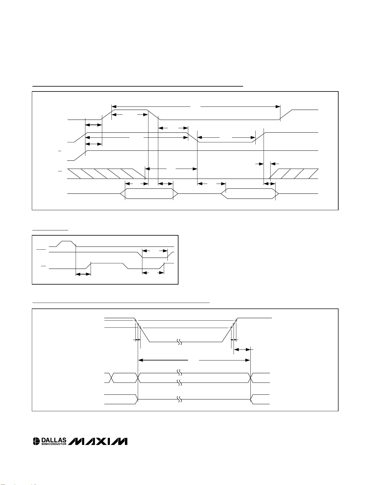
COUNTDOWN
CHAIN
X1
X2
CRYSTAL
C
L
1C
L
2
RTC REGISTERS
DS12885
Figure 1. Oscillator Circuit Showing Internal Bias Network
PARAMETER
SYMBOL
MIN
TYP
MAX
UNITS
Nominal
Frequency
f
O
kHz
Series
Resistance
ESR
kΩ
Load
Capacitance
C
L
6pF
Table 1. Crystal Specifications*
*The crystal, traces, and crystal input pins should be isolated
from RF generating signals. Refer to Application Note 58:
Crystal Considerations for Dallas Real-Time Clocks for
additional specifications.
32.768
50
Page 12

DS12885/DS12887/DS12887A/DS12C887/DS12C887A
Real-Time Clock
12 ____________________________________________________________________
Clock Accuracy
The accuracy of the clock is dependent upon the accuracy of the crystal and the accuracy of the match
between the capacitive load of the oscillator circuit and
the capacitive load for which the crystal was trimmed.
Additional error is added by crystal frequency drift
caused by temperature shifts. External circuit noise coupled into the oscillator circuit can result in the clock running fast. Figure 2 shows a typical PC board layout for
isolation of the crystal and oscillator from noise. Refer to
Application Note 58: Crystal Considerations with Dallas
Real-Time Clocks for more detailed information.
Clock Accuracy for DS12887, DS12887A,
DS12C887, DS12C887A Only
The encapsulated DIP modules are trimmed at the factory to an accuracy of ±1 minute per month at +25°C.
Power-Down/Power-Up
Considerations
The real-time clock continues to operate, and the RAM,
time, calendar, and alarm memory locations remain
nonvolatile regardless of the VCCinput level. V
BAT
must
remain within the minimum and maximum limits when
VCCis not applied. When VCCis applied and exceeds
V
PF
(power-fail trip point), the device becomes accessi-
ble after t
REC
—if the oscillator is running and the oscillator countdown chain is not in reset (Register A). This
time allows the system to stablize after power is
applied. If the oscillator is not enabled, the oscillatorenable bit is enabled on power-up, and the device
becomes immediately accessible.
Time, Calendar, and Alarm
Locations
The time and calendar information is obtained by reading the appropriate register bytes. The time, calendar,
and alarm are set or initialized by writing the appropriate register bytes. Invalid time or date entries result in
undefined operation. The contents of the 10 time, calendar, and alarm bytes can be either binary or binarycoded decimal (BCD) format.
The day-of-week register increments at midnight, incrementing from 1 through 7. The day-of-week register is
used by the daylight saving function, so the value 1 is
defined as Sunday. The date at the end of the month is
automatically adjusted for months with fewer than 31
days, including correction for leap years.
Before writing the internal time, calendar, and alarm registers, the SET bit in Register B should be written to logic
1 to prevent updates from occurring while access is
being attempted. In addition to writing the 10 time, calendar, and alarm registers in a selected format (binary or
BCD), the data mode bit (DM) of Register B must be set
to the appropriate logic level. All 10 time, calendar, and
alarm bytes must use the same data mode. The SET bit
in Register B should be cleared after the data mode bit
has been written to allow the RTC to update the time and
calendar bytes. Once initialized, the RTC makes all
updates in the selected mode. The data mode cannot be
changed without reinitializing the 10 data bytes. Tables
2A and 2B show the BCD and binary formats of the time,
calendar, and alarm locations.
The 24-12 bit cannot be changed without reinitializing the
hour locations. When the 12-hour format is selected, the
higher-order bit of the hours byte represents PM when it
is logic 1. The time, calendar, and alarm bytes are always
accessible because they are double-buffered. Once per
second the seven bytes are advanced by one second
and checked for an alarm condition.
If a read of the time and calendar data occurs during
an update, a problem exists where seconds, minutes,
hours, etc., may not correlate. The probability of reading incorrect time and calendar data is low. Several
methods of avoiding any possible incorrect time and
calendar reads are covered later in this text.
LOCAL GROUND PLANE (TOP LAYER)
CRYSTAL
GND
X2
X1
NOTE: AVOID ROUTING SIGNAL LINES
IN THE CROSSHATCHED AREA
(UPPER LEFT QUADRANT) OF
THE PACKAGE UNLESS THERE IS
A GROUND PLANE BETWEEN THE
SIGNAL LINE AND THE DEVICE PACKAGE.
Figure 2. Layout Example
Page 13

DS12885/DS12887/DS12887A/DS12C887/DS12C887A
Real-Time Clock
____________________________________________________________________ 13
The three alarm bytes can be used in two ways. First,
when the alarm time is written in the appropriate hours,
minutes, and seconds alarm locations, the alarm interrupt is initiated at the specified time each day, if the
alarm-enable bit is high. In this mode, the “0” bits in the
alarm registers and the corresponding time registers
must always be written to 0 (Table 2A and 2B). Writing
the 0 bits in the alarm and/or time registers to 1 can
result in undefined operation.
The second use condition is to insert a “don’t care”
state in one or more of the three alarm bytes. The don’tcare code is any hexadecimal value from C0 to FF. The
two most significant bits of each byte set the don’t-care
condition when at logic 1. An alarm is generated each
hour when the don’t-care bits are set in the hours byte.
Similarly, an alarm is generated every minute with
don’t-care codes in the hours and minute alarm bytes.
The don’t-care codes in all three alarm bytes create an
interrupt every second.
All 128 bytes can be directly written or read, except for
the following:
1) Registers C and D are read-only.
2) Bit 7 of register A is read-only.
3) The MSB of the seconds byte is read-only.
Table 2A. Time, Calendar, and Alarm Data Modes—BCD Mode (DM = 0)
ADDRESS
BIT 4
FUNCTION RANGE
00H 0 10 Seconds Seconds Seconds 00–59
01H 0 10 Seconds Seconds
00–59
02H 0 10 Minutes Minutes Minutes 00–59
03H 0 10 Minutes Minutes
00–59
0
04H
0
0
10 Hours
Hours Hours
1–12 +AM/PM
00–23
0
05H
0
0
10 Hours
Hours
1–12 +AM/PM
00–23
06H 0 0 0 0 0 Day Day 01–07
07H 0 0 10 Date Date Date 01–31
08H 0 0 0
Month Month 01–12
09H 10 Years Year Year 00–99
0AH UIP
DV0 RS3
Control —
0BH SET
UIE
Control —
0CH IRQF
AF UF 0 0 0 0 Control —
0DH VRT 0 0 0 0 0 0 0 Control —
0EH-31H
X X X X X X X X RAM —
32H 10 Century Century Century* 00–99
33H-7FH
X X X X X X X X RAM —
X = Read/Write Bit.
*DS12C887, DS12C887A only. General-purpose RAM on DS12885, DS12887, and DS12887A.
Note: Unless otherwise specified, the state of the registers is not defined when power is first applied. Except for the seconds register, 0 bits in the time and date registers can be written to 1, but may be modified when the clock updates. 0 bits should always be
written to 0 except for alarm mask bits.
BIT 7 BIT 6 BIT 5
AM/PM
AM/PM
10 Hours
10 Hours
BIT 3 BIT 2 BIT 1 BIT 0
Seconds Alarm
Minutes Alarm
Hours Alarm
10 Months
DV2 DV1
PIE AIE
PF
SQWE DM 24/12 DSE
RS2 RS1 RS0
Page 14

DS12885/DS12887/DS12887A/DS12C887/DS12C887A
Real-Time Clock
14 ____________________________________________________________________
Table 2B. Time, Calendar, and Alarm Data Modes—Binary Mode (DM = 1)
ADDRESS
BIT 4 BIT 3
FUNCTION RANGE
00H 0 0 Seconds Seconds 00–3B
01H 0 0 Seconds
00–3B
02H 0 0 Minutes Minutes 00–3B
03H 0 0 Minutes
00–3B
0 Hours
04H
0
00
Hours
Hours
01–0C +AM/PM
00–17
0 Hours
05H
0
0
0
Hours
01–0C +AM/PM
00–17
06H 0 0 0 0 0 Day Day 01–07
07H 0 0 0 Date Date 01–1F
08H 0 0 0 0 Month Month 01–0C
09H 0 Year Year 00–63
0AH UIP
DV0 RS3
RS0 Control —
0BH SET
UIE
Control —
0CH IRQF PF
UF 0 0 0 0 Control —
0DH VRT 0 0 0 0 0 0 0 Control —
0EH-31H
X X X X X X X X RAM —
32H N/A N/A Century* —
33H-7FH
X X X X X X X X RAM —
X = Read/Write Bit.
*DS12C887, DS12C887A only. General-purpose RAM on DS12885, DS12887, and DS12887A.
Note: Unless otherwise specified, the state of the registers is not defined when power is first applied. Except for the seconds register, 0 bits in the time and date registers can be written to 1, but may be modified when the clock updates. 0 bits should always be
written to 0 except for alarm mask bits.
BIT 7 BIT 6 BIT 5
AM/PM
AM/PM
DV2 DV1
PIE AIE
AF
BIT 2 BIT 1 BIT 0
Seconds Alarm
Minutes Alarm
Hours Alarm
RS2 RS1
SQWE DM 24/12 DSE
Page 15

DS12885/DS12887/DS12887A/DS12C887/DS12C887A
Real-Time Clock
____________________________________________________________________ 15
Bit 7: Update-In-Progress (UIP). This bit is a status
flag that can be monitored. When the UIP bit is a 1, the
update transfer occurs soon. When UIP is a 0, the
update transfer does not occur for at least 244µs. The
time, calendar, and alarm information in RAM is fully
available for access when the UIP bit is 0. The UIP bit is
read-only and is not affected by RESET. Writing the
SET bit in Register B to a 1 inhibits any update transfer
and clears the UIP status bit.
Bits 6, 5, and 4: DV2, DV1, DV0. These three bits are
used to turn the oscillator on or off and to reset the
countdown chain. A pattern of 010 is the only combination of bits that turn the oscillator on and allow the RTC
to keep time. A pattern of 11x enables the oscillator but
holds the countdown chain in reset. The next update
occurs at 500ms after a pattern of 010 is written to DV0,
DV1, and DV2.
Bits 3 to 0: Rate Selector (RS3, RS2, RS1, RS0).
These four rate-selection bits select one of the 13 taps
on the 15-stage divider or disable the divider output.
The tap selected can be used to generate an output
square wave (SQW pin) and/or a periodic interrupt. The
user can do one of the following:
1) Enable the interrupt with the PIE bit;
2) Enable the SQW output pin with the SQWE bit;
3) Enable both at the same time and the same rate;
or
4) Enable neither.
Table 3 lists the periodic interrupt rates and the squarewave frequencies that can be chosen with the RS bits.
These four read/write bits are not affected by RESET.
BIT 7 BIT 6 BIT 5 BIT 4 BIT 3 BIT 2 BIT 1 BIT 0
UIP DV2 DV1 DV0 RS3 RS2 RS1 RS0
Control Register A
Control Registers
The real-time clocks have four control registers that are
accessible at all times, even during the update cycle.
MSB LSB
Page 16

DS12885/DS12887/DS12887A/DS12C887/DS12C887A
Real-Time Clock
16 ____________________________________________________________________
Bit 7: SET. When the SET bit is 0, the update transfer
functions normally by advancing the counts once per
second. When the SET bit is written to 1, any update
transfer is inhibited, and the program can initialize the
time and calendar bytes without an update occurring in
the midst of initializing. Read cycles can be executed in
a similar manner. SET is a read/write bit and is not
affected by RESET or internal functions of the device.
Bit 6: Periodic Interrupt Enable (PIE). The PIE bit is a
read/write bit that allows the periodic interrupt flag (PF) bit
in Register C to drive the IRQ pin low. When the PIE bit is
set to 1, periodic interrupts are generated by driving the
IRQ pin low at a rate specified by the RS3–RS0 bits of
Register A. A 0 in the PIE bit blocks the IRQ output from
being driven by a periodic interrupt, but the PF bit is still
set at the periodic rate. PIE is not modified by any internal
device functions, but is cleared to 0 on RESET.
Bit 5: Alarm Interrupt Enable (AIE). This bit is a
read/write bit that, when set to 1, permits the alarm flag
(AF) bit in Register C to assert IRQ. An alarm interrupt
occurs for each second that the three time bytes equal
the three alarm bytes, including a don’t-care alarm
code of binary 11XXXXXX. The AF bit does not initiate
the IRQ signal when the AIE bit is set to 0. The internal
functions of the device do not affect the AIE bit, but is
cleared to 0 on RESET.
Bit 4: Update-Ended Interrupt Enable (UIE). This bit is
a read/write bit that enables the update-end flag (UF)
bit in Register C to assert IRQ. The RESET pin going
low or the SET bit going high clears the UIE bit.
The internal functions of the device do not affect the
UIE bit, but is cleared to 0 on RESET.
Bit 3: Square-Wave Enable (SQWE). When this bit is
set to 1, a square-wave signal at the frequency set by
the rate-selection bits RS3–RS0 is driven out on the SQW
pin. When the SQWE bit is set to 0, the SQW pin is held
low. SQWE is a read/write bit and is cleared by RESET.
SQWE is low if disabled, and is high impedance when
VCCis below VPF. SQWE is cleared to 0 on RESET.
Bit 2: Data Mode (DM). This bit indicates whether time
and calendar information is in binary or BCD format.
The DM bit is set by the program to the appropriate format and can be read as required. This bit is not modified by internal functions or RESET. A 1 in DM signifies
binary data, while a 0 in DM specifies BCD data.
Bit 1: 24/12. The 24/12 control bit establishes the format of the hours byte. A 1 indicates the 24-hour mode
and a 0 indicates the 12-hour mode. This bit is
read/write and is not affected by internal functions or
RESET.
Bit 0: Daylight Saving Enable (DSE). This bit is a
read/write bit that enables two daylight saving adjustments when DSE is set to 1. On the first Sunday in
April, the time increments from 1:59:59 AM to 3:00:00
AM. On the last Sunday in October when the time first
reaches 1:59:59 AM, it changes to 1:00:00 AM. When
DSE is enabled, the internal logic test for the first/last
Sunday condition at midnight. If the DSE bit is not set
when the test occurs, the daylight saving function does
not operate correctly. These adjustments do not occur
when the DSE bit is 0. This bit is not affected by internal
functions or RESET.
BIT 7 BIT 6 BIT 5 BIT 4 BIT 3 BIT 2 BIT 1 BIT 0
SET PIE AIE UIE SQWE DM 24/12 DSE
Control Register B
MSB LSB
Page 17

DS12885/DS12887/DS12887A/DS12C887/DS12C887A
Real-Time Clock
____________________________________________________________________ 17
Bit 7: Interrupt Request Flag (IRQF). This bit is set to
1 when any of the following are true:
PF = PIE = 1
AF = AIE = 1
UF = UIE = 1
Any time the IRQF bit is 1, the IRQ pin is driven low.
This bit can be cleared by reading Register C or with a
RESET.
Bit 6: Periodic Interrupt Flag (PF). This bit is readonly and is set to 1 when an edge is detected on the
selected tap of the divider chain. The RS3 through RS0
bits establish the periodic rate. PF is set to 1 independent of the state of the PIE bit. When both PF and PIE
are 1s, the IRQ signal is active and sets the IRQF bit.
This bit can be cleared by reading Register C or with a
RESET.
Bit 5: Alarm Interrupt Flag (AF). A 1 in the AF bit indicates that the current time has matched the alarm time.
If the AIE bit is also 1, the IRQ pin goes low and a 1
appears in the IRQF bit. This bit can be cleared by
reading Register C or with a RESET.
Bit 5: Update-Ended Interrupt Flag (UF). This bit is
set after each update cycle. When the UIE bit is set to
1, the 1 in UF causes the IRQF bit to be a 1, which
asserts the IRQ pin. This bit can be cleared by reading
Register C or with a RESET.
Bits 3 to 0: Unused. These bits are unused in Register
C. These bits always read 0 and cannot be written.
BIT 7 BIT 6 BIT 5 BIT 4 BIT 3 BIT 2 BIT 1 BIT 0
IRQFPFAFUF0000
Control Register C
BIT 7 BIT 6 BIT 5 BIT 4 BIT 3 BIT 2 BIT 1 BIT 0
VRT0000000
Control Register D
Bit 7: Valid RAM and Time (VRT). This bit indicates
the condition of the battery connected to the V
BAT
pin.
This bit is not writeable and should always be 1 when
read. If a 0 is ever present, an exhausted internal lithium energy source is indicated and both the contents of
the RTC data and RAM data are questionable. This bit
is unaffected by RESET.
Bits 6 to 0: Unused. The remaining bits of Register D
are not usable. They cannot be written and they always
read 0.
MSB LSB
MSB LSB
Page 18

DS12885/DS12887/DS12887A/DS12C887/DS12C887A
Real-Time Clock
18 ____________________________________________________________________
Century Register
(DS12C887/DS12C887A Only)
The century register at location 32h is a BCD register
designed to automatically load the BCD value 20 as the
year register changes from 99 to 00. The MSB of this
register is not affected when the load of 20 occurs, and
remains at the value written by the user.
Nonvolatile RAM (NV RAM)
The general-purpose NV RAM bytes are not dedicated
to any special function within the device. They can be
used by the processor program as battery-backed
memory and are fully available during the update cycle.
Interrupts
The RTC family includes three separate, fully automatic
sources of interrupt for a processor. The alarm interrupt
can be programmed to occur at rates from once per
second to once per day. The periodic interrupt can be
selected for rates from 500ms to 122µs. The updateended interrupt can be used to indicate to the program
that an update cycle is complete. Each of these independent interrupt conditions is described in greater
detail in other sections of this text.
The processor program can select which interrupts, if
any, are to be used. Three bits in Register B enable the
interrupts. Writing a logic 1 to an interrupt-enable bit
permits that interrupt to be initiated when the event
occurs. A 0 in an interrupt-enable bit prohibits the IRQ
pin from being asserted from that interrupt condition. If
an interrupt flag is already set when an interrupt is
enabled, IRQ is immediately set at an active level,
although the interrupt initiating the event may have
occurred earlier. As a result, there are cases where the
program should clear such earlier initiated interrupts
before first enabling new interrupts.
When an interrupt event occurs, the relating flag bit is
set to logic 1 in Register C. These flag bits are set independent of the state of the corresponding enable bit in
Register B. The flag bit can be used in a polling mode
without enabling the corresponding enable bits. The
interrupt flag bit is a status bit that software can interrogate as necessary. When a flag is set, an indication is
given to software that an interrupt event has occurred
since the flag bit was last read; however, care should
be taken when using the flag bits as they are cleared
each time Register C is read. Double latching is included with Register C so that bits that are set remain stable throughout the read cycle. All bits that are set (high)
are cleared when read, and new interrupts that are
pending during the read cycle are held until after the
cycle is completed. One, two, or three bits can be set
when reading Register C. Each used flag bit should be
examined when Register C is read to ensure that no
interrupts are lost.
The second flag bit method is used with fully enabled
interrupts. When an interrupt flag bit is set and the corresponding interrupt-enable bit is also set, the IRQ pin is
asserted low. IRQ is asserted as long as at least one of
the three interrupt sources has its flag and enable bits
set. The IRQF bit in Register C is a 1 whenever the IRQ
pin is driven low. Determination that the RTC initiated an
interrupt is accomplished by reading Register C. A logic
1 in bit 7 (IRQF bit) indicates that one or more interrupts
have been initiated by the device. The act of reading
Register C clears all active flag bits and the IRQF bit.
Oscillator Control Bits
When the DS12887, DS12887A, DS12C887, and
DS12C887A are shipped from the factory, the internal
oscillator is turned off. This prevents the lithium energy
cell from being used until the device is installed in a
system.
A pattern of 010 in bits 4 to 6 of Register A turns the
oscillator on and enables the countdown chain. A pattern of 11x (DV2 = 1, DV1 = 1, DV0 = X) turns the oscillator on, but holds the countdown chain of the oscillator
in reset. All other combinations of bits 4 to 6 keep the
oscillator off.
Square-Wave Output Selection
Thirteen of the 15 divider taps are made available to a 1of-16 multiplexer, as shown in the functional diagram.
The square-wave and periodic-interrupt generators
share the output of the multiplexer. The RS0–RS3 bits in
Register A establish the output frequency of the multiplexer (see Table 1). Once the frequency is selected, the
output of the SQW pin can be turned on and off under
program control with the square-wave enable bit, SQWE.
Periodic Interrupt Selection
The periodic interrupt causes the IRQ pin to go to an
active state from once every 500ms to once every 122µs.
This function is separate from the alarm interrupt, which
can be output from once per second to once per day.
The periodic interrupt rate is selected using the same
Register A bits that select the square-wave frequency
(Table 1). Changing the Register A bits affects the
square-wave frequency and the periodic-interrupt output. However, each function has a separate enable bit in
Register B. The SQWE bit controls the square-wave output. Similarly, the PIE bit in Register B enables the periodic interrupt. The periodic interrupt can be used with
software counters to measure inputs, create output intervals, or await the next needed software function.
Page 19

DS12885/DS12887/DS12887A/DS12C887/DS12C887A
Real-Time Clock
____________________________________________________________________ 19
Update Cycle
The device executes an update cycle once per second
regardless of the SET bit in Register B. When the SET
bit in Register B is set to 1, the user copy of the doublebuffered time, calendar, and alarm bytes is frozen and
does not update as the time increments. However, the
time countdown chain continues to update the internal
copy of the buffer. This feature allows time to maintain
accuracy independent of reading or writing the time,
calendar, and alarm buffers, and also guarantees that
time and calendar information is consistent. The update
cycle also compares each alarm byte with the corre-
sponding time byte and issues an alarm if a match or if
a don’t-care code is present in all three positions.
There are three methods that can handle RTC access
that avoid any possibility of accessing inconsistent time
and calendar data. The first method uses the updateended interrupt. If enabled, an interrupt occurs after
every update cycle that indicates over 999ms is available to read valid time and date information. If this
interrupt is used, the IRQF bit in Register C should be
cleared before leaving the interrupt routine.
A second method uses the update-in-progress bit (UIP)
in Register A to determine if the update cycle is in
progress. The UIP bit pulses once per second. After
the UIP bit goes high, the update transfer occurs 244µs
later. If a low is read on the UIP bit, the user has at least
244µs before the time/calendar data is changed.
Therefore, the user should avoid interrupt service routines that would cause the time needed to read valid
time/calendar data to exceed 244µs.
The third method uses a periodic interrupt to determine if
an update cycle is in progress. The UIP bit in Register A
is set high between the setting of the PF bit in Register C
(Figure 3). Periodic interrupts that occur at a rate greater
than t
BUC
allow valid time and date information to be
reached at each occurrence of the periodic interrupt.
The reads should be complete within one (t
PI/2
+ t
BUC
)
to ensure that data is not read during the update cycle.
Handling, PC Board Layout,
and Assembly
The EDIP module can be successfully processed
through conventional wave-soldering techniques so long
as temperature exposure to the lithium energy source
does not exceed +85°C. Post-solder cleaning with waterwashing techniques is acceptable, provided that ultrasonic vibration is not used. Such cleaning can damage
the crystal.
SELECT BITS
REGISTER A
RS3
tPI PERIODIC
INTERRUPT
RATE
SQW OUTPUT
FREQUENCY
0 0 0 0 None None
0001
256Hz
0 0 1 0 7.8125ms 128Hz
0011
8.192kHz
0100
4.096kHz
0101
2.048kHz
0110
1.024kHz
0111
512Hz
1000
256Hz
1 0 0 1 7.8125ms 128Hz
1 0 1 0 15.625ms 64Hz
1 0 1 1 31.25ms 32Hz
1 1 0 0 62.5ms 16Hz
1 1 0 1 125ms 8Hz
1 1 1 0 250ms 4Hz
1 1 1 1 500ms 2Hz
Table 3. Periodic Interrupt Rate and
Square-Wave Output Frequency
UIP
UF
PF
t
BUC
= DELAY TIME BEFORE UPDATE
CYCLE = 244µs
1 SECOND
t
PI
t
P1/2
t
P1/2
t
BUC
Figure 3. UIP and Periodic Interrupt Timing
RS2 RS1 RS0
3.90625ms
122.070µs
244.141µs
488.281µs
976.5625µs
1.953125ms
3.90625ms
Page 20

DS12885/DS12887/DS12887A/DS12C887/DS12C887A
Real-Time Clock
20 ____________________________________________________________________
24
23
22
21
20
19
18
17
1
2
3
4
5
6
7
8
V
CC
SQW
N.C.
RCLRAD0
X2
X1
MOT
TOP VIEW
V
BAT
IRQ
RESET
DSAD4
AD3
AD2
AD1
16
15
14
13
9
10
11
12
GND
R/W
AS
CSGND
AD7
AD6
AD5
SO, PDIP
PLCC
DS12885
DS12885S
DS12885Q
V
CC
SQW
N.C.
N.C.
(RCLR)
AD0
N.C.
N.C.
MOT
N.C.
IRQ
RESET
DSAD4
AD3
AD2
AD1
N.C.
R/W
AS
CS
( ) FOR THE DS12887A/DS12C887A.
NOTE: THE DS12887A AND DS12C887A CANNOT BE STORED OR SHIPPED IN CONDUCTIVE MATERIAL
THAT WILL GIVE A CONTINUITY PATH BETWEEN THE RAM CLEAR PIN AND GROUND.
GND
AD7
AD6
AD5
EDIP
DS12887
DS12887A
DS12C887
DS12C887A
12
13
14
15
16
17
18
1N.C.
V
CC
SQW
N.C.
MOT
X1
X2
GND
CS
AS
N.C.
AD7
N.C.
AD6
2
3
4
26
27
28
19
20
21
22
23
24
25
5
6
7
8
9
10
11
AD0
AD1
AD2
AD3
AD4
AD5
N.C.
RCLR
V
BAT
IRQ
RESET
DS
GND
R/W
1
2
3
4
5
6
7
8
9
10
11
12
24
23
22
21
20
19
18
17
16
15
14
13
Pin Configurations
Page 21

DS12885/DS12887/DS12887A/DS12C887/DS12C887A
Real-Time Clock
____________________________________________________________________ 21
PACKAGE
PDIP 75 30
SO 105 22
PLCC 95 25
Thermal Information
Chip Information
TRANSISTOR COUNT: 17,000
PROCESS: CMOS
SUBSTRATE CONNECTED TO GROUND
TQFP
TOP VIEW
32 28
293031
25
26
27
X2
X1
MOT
V
CC
N.C.
N.C.
SQW
N.C.
10
13
15
14
1611 12
9
AD6
AD7
N.C.
CS
GND
N.C.
AS
R/W
17
18
19
20
21
22
23
N.C.
24 RCLR
V
BAT
IRQ
N.C.
RESET
DS
GND
2
3
4
5
6
7
8AD5
AD4
N.C.
AD3
N.C.
AD2
AD1
1AD0
DS12885T
Pin Configurations (continued) Ordering Information
PART
TEMP RANGE
PIN-
TOP
MARK*
DS12885
24 PDIP DS12885
DS12885N
24 PDIP
DS12885N
DS12885Q
28 PLCC
DS12885Q
DS12885Q+
28 PLCC
DS12885Q
DS12885QN
28 PLCC
DS12885Q
DS12885QN+
28 PLCC
DS12885Q
DS12885S
24 SO
(300 mils)
DS12885S
DS12885S+
24 SO
(300 mils)
DS12885S
DS12885SN
24 SO
(300 mils)
DS12885S
DS12885SN+
24 SO
(300 mils)
DS12885S
DS12885T
32 TQFP
DS12885T
DS12885TN
32 TQFP
DS12885T
DS12887
24 EDIP DS12887
DS12887A
24 EDIP
DS12887A
DS12887A+
24 EDIP
DS12887A
DS12C887
24 EDIP
DS12C887
DS12C887A
24 EDIP
DS12C887
DS12C887A+
24 EDIP
DS12C887
+Denotes a lead-free/RoHS-compliant device.
*A “+” anywhere on the top mark indicates a lead-free device,
and an “N” indicates an industrial temperature range device.
THETA-JA (°C/W) THETA-JC (°C/W)
PACKAGE
0°C to +70°C
-40°C to +85°C
0°C to +70°C
0°C to +70°C
-40°C to +85°C
-40°C to +85°C
0°C to +70°C
0°C to +70°C
-40°C to +85°C
-40°C to +85°C
0°C to +70°C
-40°C to +85°C
0°C to +70°C
0°C to +70°C
0°C to +70°C
0°C to +70°C
0°C to +70°C
0°C to +70°C
Page 22

DS12885/DS12887/DS12887A/DS12C887/DS12C887A
Real-Time Clock
22 ____________________________________________________________________
Package Information
For the latest package outline information, go to www.maxim-ic.com/DallasPackInfo.
56-G4009-001.EPS
Page 23

DS12885/DS12887/DS12887A/DS12C887/DS12C887A
Real-Time Clock
____________________________________________________________________ 23
56-G5000-003.EPS
Package Information (continued)
For the latest package outline information, go to www.maxim-ic.com/DallasPackInfo.
Page 24

DS12885/DS12887/DS12887A/DS12C887/DS12C887A
Real-Time Clock
24 ____________________________________________________________________
56-G0001-001.EPS
Package Information (continued)
For the latest package outline information, go to www.maxim-ic.com/DallasPackInfo.
Page 25

DS12885/DS12887/DS12887A/DS12C887/DS12C887A
Real-Time Clock
____________________________________________________________________ 25
56-G0001-001.EPS
Package Information (continued)
For the latest package outline information, go to www.maxim-ic.com/DallasPackInfo.
Page 26

DS12885/DS12887/DS12887A/DS12C887/DS12C887A
Real-Time Clock
26 ____________________________________________________________________
56-G4001-001.EPS
Package Information (continued)
For the latest package outline information, go to www.maxim-ic.com/DallasPackInfo.
Page 27

DS12885/DS12887/DS12887A/DS12C887/DS12C887A
Real-Time Clock
Maxim cannot assume responsibility for use of any circuitry other than circuitry entirely embodied in a Maxim product. No circuit patent licenses are
implied. Maxim reserves the right to change the circuitry and specifications without notice at any time.
Maxim Integrated Products, 120 San Gabriel Drive, Sunnyvale, CA 94086 408-737-7600 ____________________ 27
© 2006 Maxim Integrated Products Printed USA is a registered trademark of Maxim Integrated Products, Inc.
is a registered trademark of Dallas Semiconductor Corporation.
Quijano
56-G4004-001.EPS
Package Information (continued)
For the latest package outline information, go to www.maxim-ic.com/DallasPackInfo.
 Loading...