

Page 1
www.maxim-ic.com
DS1284/DS1286
Watchdog Timekeepers
GENERAL DESCRIPTION
The DS1284/DS1286 watchdog timekeepers are
self-contained real-time clocks, alarms, watchdog
timers, and interval timers in a 28-pin JEDEC DIP
and encapsulated DIP package. The DS1286
contains an embedded lithium energy source and a
quartz crystal, which eliminates the need for any
external circuitry. The DS1284 requires an external
quartz crystal and a V
lithium battery. Data contained within 64 8-bit
registers can be read or written in the same manner
as byte-wide static RAM. Data is maintained in the
watchdog timekeeper by intelligent control circuitry
that detects the status of V
memory when V
is out of tolerance. The lithium
CC
energy source can maintain data and real time for
over 10 years in the absence of V
timekeeper information includes hundredths of
seconds, seconds, minutes, hours, day, date, month,
and year. The date at the end of the month is
automatically adjusted for months with fewer than
31 days, including correction for leap year. The
DS1284/DS1286 operate in either 24-hour or 12hour format with an AM/PM indicator. The devices
provide alarm windows and interval timing between
0.01 seconds and 99.99 seconds. The real-time
alarm provides for preset times of up to one week.
source, which could be a
BAT
and write protects
CC
. Watchdog
CC
FEATURES
Keeps Track of Hundredths of Seconds,
Seconds, Minutes, Hours, Days, Date of the
Month, Months, and Years; Valid Leap Year
Compensation Up to 2100
Watchdog Timer Restarts an Out-of-Control
Processor
Alarm Function Schedules Real-Time-Related
Activities
Embedded Lithium Energy Cell Maintains
Time, Watchdog, User RAM, and Alarm
Information
Programmable Interrupts and Square-Wave
Outputs Maintain JEDEC Footprint
All Registers are Individually Addressable via
the Address and Data Bus
Accuracy is Better than ±1 Minute/Month at
+25°C (EDIP)
Greater than 10 Years of Timekeeping in the
Absence of V
50 Bytes of User NV RAM
Underwriters Laboratory (UL) Recognized
-40°C to +85°C Industrial Temperature Range
Option
Pin Configurations appear at end of data sheet.
CC
ORDERING INFORMATION
PART TEMP RANGE VOLTAGE (V) PIN-PACKAGE TOP MARK*
DS1284
DS1284N
DS1284Q
DS1284Q+
DS1284Q/T&R
DS1284Q+T&R
DS1284QN
DS1284QN+
DS1284QN/T&R
DS1284QN+T&R
DS1286
DS1286I
DS1286I+
+ Denotes a lead(Pb)-free/RoHS-compliant package.
* A “+” anywhere on the top mark indicates a lead-free package.
1 of 18
0°C to +70°C 5.0
-40°C to +85°C 5.0
0°C to +70°C 5.0
0°C to +70°C 5.0
0°C to +70°C 5.0
0°C to +70°C 5.0
-40°C to +85°C 5.0
-40°C to +85°C 5.0
-40°C to +85°C 5.0
-40°C to +85°C 5.0
0°C to +70°C 5.0
-40°C to +85°C 5.0
-40°C to +85°C 5.0
28 DIP (600 mils) DS1284
28 DIP (600 mils) DS1284 N
28 PLCC DS1284Q
28 PLCC DS1284Q
28 PLCC/Tape and Reel DS1284Q
28 PLCC/Tape and Reel DS1284Q
28 PLCC DS1284QN
28 PLCC DS1284QN
28 PLCC/Tape and Reel DS1284QN
28 PLCC/Tape and Reel DS1284QN
28 EDIP (720 mils) DS1286
28 EDIP (720 mils) DS1286 IND
28 EDIP (720 mils) DS1286 IND
REV: 032406
Page 2

DS1284/DS1286
OPERATION—READ REGISTERS
The DS1284/DS1286 execute a read cycle whenever WE (write enable) is inactive (high) and CE (chip
enable) and OE (output enable) are active (low). The unique address specified by the six address inputs
(A0–A5) defines which of the 64 registers is to be accessed. Valid data is available to the eight data
output drivers within t
(access time) after the last address input signal is stable, provided that CE and
ACC
OE access times are also satisfied. If OE and CE access times are not satisfied, then data access must be
measured from the latter occurring signal (CE or OE) and the limiting parameter is either t
for CE or t
CO
OE
for OE rather than address access.
OPERATION—WRITE REGISTERS
The DS1284/DS1286 are in the write mode whenever the WE and CE signals are in the active-low state
after the address inputs are stable. The latter occurring falling edge of CE or WE determines the start of
the write cycle. The write cycle is terminated by the earlier rising edge of CE or WE. All address inputs
must be kept valid throughout the write cycle. WE must return to the high state for a minimum recovery
state (t
) before another cycle can be initiated. Data must be valid on the data bus with sufficient data
WR
setup (tDS) and data hold time (tDH) with respect to the earlier rising edge of CE or WE. The OE control
signal should be kept inactive (high) during write cycles to avoid bus contention. However, if the output
bus has been enabled (CE and OE active), then WE will disable the outputs in t
from its falling edge.
ODW
DATA RETENTION
The watchdog timekeeper provides full functional capability when V
maintained in the absence of V
without any additional support circuitry. The DS1284/DS1286
CC
constantly monitor VCC. Should the supply voltage decay, the watchdog timekeeper automatically write
protects itself, and all inputs to the registers become “don’t care.” Both INTA and INTB (INTB) are
open-drain outputs. The two interrupts and the internal clock continue to run regardless of the level of
VCC. However, it is important to ensure that the pullup resistors used with the interrupt pins are never
pulled up to a value greater than V
+ 0.3V. As VCC falls below the battery voltage, a power-switching
CC
circuit turns on the lithium energy source to maintain the clock and timer data functionality. Also ensure
that during this time (battery-backup mode), the voltage present at INTA and INTB (INTB) never
exceeds the battery voltage. If the active-high mode is selected for INTB (INTB), this pin only goes high
in the presence of V
. During power-up, when V
CC
circuit connects external V
exceeds V
V
CC
TP
for t
REC
.
and disconnects the V
CC
rises above approximately 3.0V, the power-switching
CC
energy source. Normal operation can resume after
BAT
is greater than V
CC
. Data is
TP
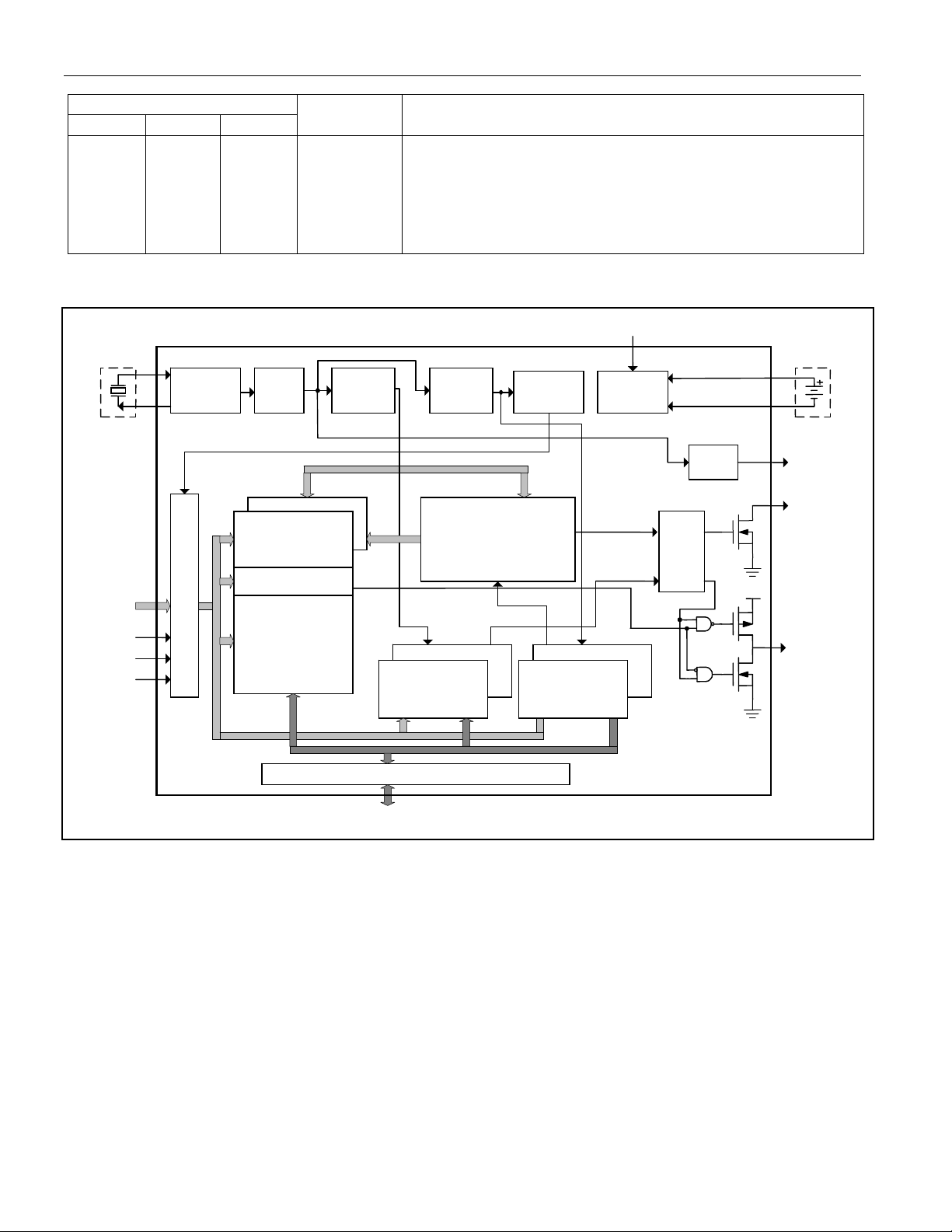
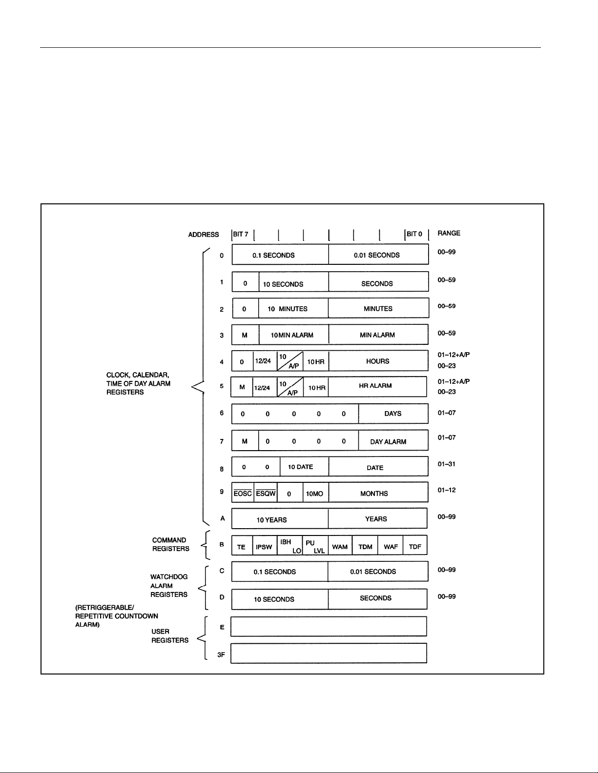
WATCHDOG TIMEKEEPER REGISTERS
The watchdog timekeeper has 64 8-bits-wide registers that contain all the timekeeping, alarm, watchdog,
control, and data information. The clock, calendar, alarm, and watchdog registers are memory locations
that contain external (user-accessible) and internal copies of the data. The external copies are independent
of internal functions, except that they are updated periodically by the simultaneous transfer of the
incremented internal copy (see Figure 1). The command register bits are affected by both internal and
external functions. This register is discussed later. The 50 bytes of RAM registers can only be accessed
from the external address and data bus. Registers 0, 1, 2, 4, 6, 8, 9, and A contain time-of-day and date
information (see Figure 2). Time-of-day information is stored in binary-coded decimal (BCD). Registers
3, 5, and 7 contain the time-of-day alarm information. Time-of-day alarm information is stored in BCD.
Register B is the command register and information in this register is binary. Registers C and D are the
watchdog alarm registers and information stored in these two registers is in BCD. Registers E to 3F are
user bytes and can be used to contain data at the user’s discretion.
2 of 18
Page 3

PIN DESCRIPTION
PIN
DIP EDIP PLCC
1 1 1
2, 3 — 2, 3 X1, X2
2, 3, 4,
4
21, 24,
4 N.C. No Connection
25
5–10 5–10 5–10 A5–A0 Address Inputs
11, 12,
13, 15,
16–19
11, 12,
13, 15,
16–19
11, 12,
13, 15,
16–19
14, 21 14 14, 21 GND Ground
20 20 20
22 22 22
23 23 23 SQW
24 — 24
25 — 25 V
26 26 26
27 27 27
NAME FUNCTION
INTA
Active-Low Interrupt Outp
pullup resistor for proper operation.
Connections for Standard 32.768kHz Quartz Crystal. The internal
oscillator circuitry is designed for operation with a crystal having
a specified load capacitance (C
directly to the X1 and X2 pins. There is no need for external
capacitors or resistors. For more information on crystal selection
and crystal layout considerations, refer to Application Note 58:
Crystal Considerations with Dallas Real Time Clocks.
DQ0, DQ1,
DQ2, DQ3,
Data Input/Output
DQ4–DQ7
CE
OE
Active-Low Chip-Enable Input
Active-Low Output-Enable Input
Square-Wave Output. Push-pull output. High impedance when
V
is below VTP.
CC
Active-Low RAM Clear. Used to clear (set to logic 1) all 50
bytes of user NV RAM, but does not affect the registers
involved with time, alarm, and watchdog functions. To clear the
RAM, RCLR must be forced to an input logic 0 (-0.3V to
RCLR
+0.8V) during battery-backup mode when V
The RCLR function is designed to be used via human interface
(shorting to ground or by switch) and not be driven with external
buffers. This pin is internally pulled up and should be left
floating when not in use.
Input for Any Standard 3V Lithium Cell or Other Energy
Source. Input voltage must be held between the minimum and
maximum limits for proper operation. The supply should be
connected directly to the V
BAT
in series with the battery to the V
not necessary because reverse charging current-protection
circuitry is provided internal to the device and has passed the
requirements of Underwriters Laboratories for UL listing. This
pin should be grounded but can be left floating.
Active-Low (Active-High) Interrupt Output B. When the activehigh state is selected (IBH = 1), an open-drain pullup transistor
connected to V
INTB
(INTB)
When the active-low state is selected (IBH = 0), an open-drain
pulldown transistor connected to ground sinks current when the
output is active. If active-high output operation is selected, a
pulldown resistor is required for proper operation. When activelow output operation is selected, a pullup resistor is required for
proper operation.
WE
Active-Low Write-Enable Input
3 of 18
DS1284/DS1286
ut A. This open-drain pin requires a
) of 6pF. The crystal is connected
L
is not applied.
CC
pin. A diode must not be placed
BAT
pin. Furthermore, a diode is
BAT
sources current when the output is active.
CC
Page 4
PIN
A
A
CE OE W
I
I
DIP EDIP PLCC
28 28 28 VCC
Figure 1. Block Diagram
DS1284/DS1286
NAME FUNCTION
Primary Power-Supply Input. When voltage is applied within
normal limits, the device is fully accessible and data can be
written and read. When a backup supply is connected to the
device and V
is below VTP, read and writes are inhibited.
CC
However, the timekeeping function continues unaffected by the
lower input voltage.
DS1286
only
0-A5
E
X1
X2
Oscillator
ddress Decode and Control
8
Internal Registers
External Registers,
clock, calendar,
time of day alarm
Command
Register
User RAM
50 Bytes
40.96
Watchdog Alarm
Internal Counters
Data I/O Buffers
DQ0–DQ7
40.96
Update seconds through
years and check time of
day alarm
100Hz
External
Registers
PF delay
10
Internal RegistersInternal Counters
External
Registers
Hundredths of
Seconds
TD INT
WD INT
100Hz
V
CC
V
Power
Switch
IBH
BAT
GND
Swap
pins
DS1284/DS1286
DS1286 only
4
1024Hz
SQW
NTA
N
V
CC
P
NTB
/
(INTB)
N
4 of 18
Page 5
DS1284/DS1286
HUNDREDTHS-OF-SECONDS GENERATOR
The hundredths-of-seconds generator circuit shown in the Block Diagram (Figure 1) is a state machine
that divides the incoming frequency (4096Hz) by 41 for 24 cycles and 40 for 1 cycle. This produces a
100Hz output that is slightly off during the short term, and is exactly correct every 250ms. The divide
ratio is given by:
Ratio = [41 x 24 + 40 x 1] / 25 = 40.96
Thus, the long-term average frequency output is exactly 100Hz.
Figure 2. Watchdog Timekeeper Registers
5 of 18
Page 6

DS1284/DS1286
TIME-OF-DAY REGISTERS
Registers 0, 1, 2, 4, 6, 8, 9, and A contain time-of-day data in BCD. Ten bits within these eight registers
are not used and always read 0 regardless of how they are written. Bits 6 and 7 in the months register (9)
are binary bits. When set to logic 0, EOSC (bit 7) enables the RTC oscillator. This bit is set to logic 1 as
shipped from Dallas Semiconductor to prevent lithium energy consumption during storage and shipment.
The user normally turns this bit on during device initialization. However, the oscillator can be turned on
and off as necessary by setting this bit to the appropriate level. Bit 6 of this same byte controls the squarewave output (pin 23). When set to logic 0, the square-wave output pin outputs a 1024Hz square-wave
signal. When set to logic 1, the square-wave output pin is in a high-impedance state. Bit 6 of the hours
register is defined as the 12- or 24-hour select bit. When set to logic 1, the 12-hour format is selected. In
the 12-hour format, bit 5 is the AM/PM bit with logic 1 being PM. In the 24-hour mode, bit 5 is the
second 10-hour bit (20–23 hours). The time-of-day registers are updated every 0.01 seconds from the
RTC, except when the TE bit (bit 7 of register B) is set low or the clock oscillator is not running. The
preferred method of synchronizing data access to and from the watchdog timekeeper is to access the
command register by doing a write cycle to address location 0B and setting the TE (transfer enable) bit to
a logic 0. Doing so freezes the external time-of-day registers at the present recorded time, allowing access
to occur without danger of simultaneous update. When the watch registers have been read or written, a
second write cycle to location 0B, setting the TE bit to a logic 1, puts the time-of-day registers back to
being updated every 0.01 second. No time is lost in the RTC because the internal copy of the time-of-day
register buffers is continually incremented while the external memory registers are frozen.
An alternate method of reading and writing the time-of-day registers is to ignore synchronization.
However, any single read may give erroneous data as the RTC may be in the process of updating the
external memory registers as data is being read. The internal copies of seconds through years are
incremented and time-of-day alarm is checked during the period that hundreds of seconds read 99 and are
transferred to the external register when hundredths of seconds roll from 99 to 00. A way of making sure
data is valid is to do multiple reads and compare. Writing the registers can also produce erroneous results
for the same reasons. A way of making sure that the write cycle has caused proper update is to do read
verifies and re-execute the write cycle if data is not correct. While the possibility of erroneous results
from reads and write cycles has been stated, it is worth noting that the probability of an incorrect result is
kept to a minimum due to the redundant structure of the watchdog timekeeper.
TIME-OF-DAY ALARM REGISTERS
Registers 3, 5, and 7 contain the time-of-day alarm registers. Bits 3, 4, 5, and 6 of register 7 always read 0
regardless of how they are written. Bit 7 of registers 3, 5, and 7 are mask bits (Figure 3). When all the
mask bits are logic 0, a time-of-day alarm only occurs when registers 2, 4, and 6 match the values stored
in registers 3, 5, and 7. An alarm is generated every day when bit 7 of register 7 is set to logic 1.
Similarly, an alarm is generated every hour when bit 7 of registers 7 and 5 is set to logic 1. When bit 7 of
registers 7, 5, and 3 is set to logic 1, an alarm occurs every minute when register 1 (seconds) rolls from 59
to 00.
Time-of-day alarm registers are written and read in the same format as the time-of-day registers. The
time-of-day alarm flag and interrupt is always cleared when alarm registers are read or written.
6 of 18
Page 7

DS1284/DS1286
WATCHDOG ALARM REGISTERS
Registers C and D contain the time for the watchdog alarm. The two registers contain a time count from
to 99.99 seconds in BCD. The value written into the watchdog alarm registers can be written or read in
any order. Any access to Registers C or D causes the watchdog alarm to reinitialize and clears the
watchdog flag bit and the watchdog interrupt output. When a new value is entered or the watchdog
registers are read, the watchdog timer starts counting down from the entered value to 0. When 0 is
reached, the watchdog interrupt output goes to the active state. The watchdog timer countdown is
interrupted and reinitialized back to the entered value every time either of the registers is accessed. In this
manner, controlled periodic accesses to the watchdog timer can prevent the watchdog alarm from ever
going to an active level. If access does not occur, the countdown alarm is repetitive. The watchdog alarm
registers always read the entered value. The actual countdown register is internal and is not readable.
Writing Registers C and D to 0 disables the watchdog alarm feature.
COMMAND REGISTER (0Bh)
Bit #:
Name:
Note: The initial state of these bits is not defined.
BIT 7 BIT 6 BIT 5 BIT 4 BIT 3 BIT 2 BIT 1 BIT 0
TE IPSW IBH PU/LVL WAM TDM WAF TDF
Bit 7: Transfer Enable (TE). This bit when set to logic 1 allows the internal time and date counters to
update the user accessible registers. When set to logic 0, the external, user-accessible time and date
registers remain static when being read or written, while the internal counters continue to run. The
function of this bit is further described in the time-of-day registers section
Bit 6: Interrupt Pin Swap (IPSW). This bit directs which type of interrupt is present on interrupt pins
INTA or INTB (INTB). When set to logic 1, INTA becomes the time-of-day alarm interrupt pin and
INTB (INTB) becomes the watchdog interrupt pin. When bit 6 is set to logic 0, the interrupt functions are
reversed such that the time-of-day alarm is output on INTB (INTB) and the watchdog interrupt is output
on INTA. Caution should be exercised when dynamically setting this bit as the interrupts are reversed
even if in an active state.
Bit 5: Interrupt B Active High/Low (IBH). When bit 5 is set to logic 1, the B interrupt output sources
current when active. When bit 5 is set to logic 0, the B interrupt output sinks current when active.
Bit 4: Pulse/Level Output (PU/LVL). When set to logic 1, the pulse mode is selected and INTA sinks
current for a minimu m of 3ms and then releases. Output INTB (INTB) either sinks or sources current for
a minimum of 3ms depending on the level of bit 5. The watchdog timer continues to run and WAF is
cleared at the end of the pulse. When set to a logic 0, both INTA and INTB (INTB), when active, output
an active low (INTB (INTB) active high when IBH = 1) until the interrupt is cleared.
Bit 3: Watchdog Alarm Mask (WAM). When this bit is written to logic 1, the watchdog interrupt
output is deactivated regardless of the state of WAF. When WAM is set to logic 0 and the WAF bit is set
to a 1, the watchdog interrupt output goes to the active state, which is determined by bits 1, 4, 5, and 6 of
the command register.
Bit 2: Time-of-Day Alarm Mask (TDM). When this bit is written to logic 1, the time-of-day alarminterrupt output is deactivated regardless of the state of TDF. When TDM is set to logic 0, the time-of-day
7 of 18
Page 8

DS1284/DS1286
interrupt output goes to the active state, which is determined by bits 0, 4, 5, and 6 of the command
register.
Bit 1: Watchdog Alarm Flag (WAF). When this bit is set internally to logic 1, a watchdog alarm has
occurred. This bit is read-only and writing this register has no effect on the bit. The bit is reset when any
of the watchdog alarm registers are accessed. The WAM bit has no effect on the operation of this bit. If
pulse mode (PU/LVL = 1) is selected, the watchdog continues to run and the flag is internally written to 0
at the end of the pulse. The WAM bit has no effect on the operation of this bit.
Bit 0: Time-of-Day Alarm Flag (TDF). When this bit is set internally to a logic 1, indicates that a match
with the time-of-day alarm registers has occurred. This bit is read-only and writing this register has no
effect on the bit. The time of the alarm can be determined by reading the time-of-day alarm registers. The
bit is reset when any of the time-of-day alarm registers are read. The TDM bit has no effect on the
operation of this bit.
Figure 3. Time-of-Day Alarm Mask Bits
REGISTER
(03h)
MINUTES
(05h)
HOURS
(07h)
DAYS
FUNCTION
1 1 1 Alarm once per minute
0 1 1 Alarm when minutes match
0 0 1 Alarm when hours and minutes match
0 0 0 Alarm when hours, minutes, and days match
8 of 18
Page 9

DS1284/DS1286
ABSOLUTE MAXIMUM RATINGS
Voltage Range on Any Pin Relative to Ground……………………………………………..-0.3V to +7.0V
Operating Temperature Range
Commercial………………………………………………………………………………..0C to +70C
Industrial………………………………………………………………………………...-40°C to +85°C
Storage Temperature Range………………………………………………………………...-40°C to +85°C
Soldering Temperature………………..……………...See IPC/JEDEC J-STD-020 Specification (Note 13)
Stresses beyond those listed as “Absolute Maxim Ratings” may cause permanent damage to the device. These are stress ratings only, any
functional operation of the device at these or any other conditions beyond the those indicated in operations section of the specifications is no
implied. Exposure to absolute maximum ratings for extended periods may affect device reliability.
RECOMMENDED DC OPERATING CONDITIONS
(TA = -40°C to +85°C or 0°C to +70°C.)
PARAMETER SYMBOL MIN TYP MAX UNITS NOTES
Power-Supply Voltage VCC 4.5 5.0 5.5 V 10 Input Logic 1 VIH 2.2
VCC +
0.3
V 10
Input Logic 0 VIL -0.3 +0.8 V 10
V
Input Voltage V
BAT
2.4 3.0 3.5 V 10
BAT
DC ELECTRICAL CHARACTERISTICS
(VCC = 5V 10%, TA = -40C to +85C or 0°C to +70°C.)
PARAMETER SYMBOL MIN TYP MAX UNITS NOTES
Input Leakage Current IIL -1.0 +1.0 Output Leakage Current ILO -1.0 +1.0
A
A
I/O Leakage Current
CE VIH VCC
-1.0 +1.0
LIO
A
I
Output Current at 2.4V IOH -1.0 mA
Output Current at 0.4V IOL 2.0 mA
Standby Current CE = 2.2V I
Standby Current CE > VCC - 0.5 I
3.0 7.0 mA
CCS1
4.0 mA
CCS2
Active Current ICC 15 mA
Write-Protection Voltage VTP
1.088
x V
BAT
1.26 x
V
BAT
1.324
x V
BAT
V
DC ELECTRICAL CHARACTERISTICS
(VCC = 0V, V
= 2.4V to 3.5V, T
BAT
= 0°C to +70°C.)
A
PARAMETER SYMBOL MIN TYP MAX UNITS NOTES
Battery Current (EOSC = 0)
I
+0.5 +0.6
BAT
9 of 18
A
Page 10

DS1284/DS1286
CAPACITANCE
(TA = +25°C)
PARAMETER SYMBOL MIN TYP MAX UNITS NOTES
Input Capacitance CIN 7 10 pF
Output Capacitance C
Input/Output Capacitance C
7 10 pF
OUT
7 10 pF
I/O
AC ELECTRICAL CHARACTERISTICS
(VCC = 4.5V to 5.5V, TA = -40C to +85C or 0°C to +70°C.)
PARAMETER SYMBOL MIN TYP MAX UNITS NOTES
Read Cycle Time tRC 150 ns 1 Address Access Time t
CE Access Time tCO 150 ns
OE Access Time tOE 60 ns
OE or CE to Output Active t
Output High-Z from Deselect tOD 60 ns
Output Hold from Address Change tOH 10 ns
Write Cycle Time tWC 150 ns
Write Pulse Width tWP 140 ns 3
Address Setup Time tAW 0 ns
Write Recovery Time tWR 10 ns
Output High-Z from WE t
Output Active from WE t
Data Setup Time tDS 45 ns 4
Data Hold Time tDH 0 ns 4,5
INTA, INTB Pulse Width t
150 ns
ACC
10 ns
COE
50 ns
ODW
10 ns
OEW
3 ms 11,12
IPW
10 of 18
Page 11

READ CYCLE (NOTE 1)
WRITE CYCLE 1 (NOTES 2, 6, 7)
DS1284/DS1286
11 of 18
Page 12

WRITE CYCLE 2 (NOTES 2, 8)
TIMING DIAGRAM: INTERRUPT
OUTPUTS PULSE MODE (NOTES 11, 12)
DS1284/DS1286
12 of 18
Page 13

DS1284/DS1286
POWER-UP/POWER-DOWN CONDITION
PARAMETER SYMBOL MIN TYP MAX UNITS NOTES
CE at V
VCC Slew from 4.5V to 0V (CE at VIH)
VCC Slew from 0V to 4.5V (CE at VIH)
CE at VIH after Power-Up t
POWER-DOWN/POWER-UP CONDITION
(TA = +25°C)
Expected Data-Retention Time (DS1286)
WARNING: Under no circumstances are negative undershoots, of any amplitude, allowed when device is in battery-backup mode.
before Power-Down
IH
tPD 0
tF 350
100
t
R
150 ns
REC
s
s
s
PARAMETER SYMBOL MIN TYP MAX UNITS NOTES
t
10 years 9
DR
13 of 18
Page 14

DS1284/DS1286
NOTES:
1. WE is high for a read cycle.
2. OE = VIH or VIL. If OE = VIH during write cycle, the output buffers remain in a high-impedance state.
3. t
is specified as the logical AND of CE and WE. tWP is measured from the latter of CE or WE going
WP
low to the earlier of CE or WE going high.
4. t
or tDH are measured from the earlier of CE or WE going high.
DS
5. tDH is measured from WE going high. If CE is used to terminate the write cycle, then tDH = 20ns.
6. If the CE low transition occurs simultaneously with or later than the WE low transition in write cycle
1, the output buffers remain in a high-impedance state during this period.
7. If the CE high transition occurs prior to or simultaneously with the WE high transition, the output
buffers remain in a high-impedance state during this period.
8. If WE is low or the WE low transition occurs prior to or simultaneously with the CE low transition,
the output buffers remain in a high-impedance state during this period.
9. Each DS1284/DS1286 is marked with a four-digit date code AABB. AA designates the year of
manufacture. BB designates the week of manufacture. The expected tDR is defined as starting at the
date of manufacture.
10. All voltages are referenced to ground.
11. Applies to both interrupt pins when the alarms are set to pulse.
12. Interrupt output occurs within 100ns on the alarm condition existing.
13. RTC modules can be successfully processed through conventional wave-soldering techniques as long
as temperature exposure to the lithium energy source contained within does not exceed +85°C.
However, post-solder cleaning with water-washing techniques is acceptable, provided that ultrasonic
vibrations are not used to prevent crystal damage.
AC TEST CONDITIONS
Output Load: 100pF + 1TTL Gate
Input Pulse Levels: 0 to 3.0V
Timing Measurement Reference Levels
Input: 1.5V
Output: 1.5V
Input Pulse Rise and Fall Times: 5ns
PACKAGE INFORMATION
For the latest package outline information and land patterns, go to www.maxim-ic.com/packages.
PACKAGE TYPE PACKAGE CODE DOCUMENT NO.
28 PDIP P28+9 21-0044
28 PLCC Q28+11 21-0049
28 EDIP MDP28+1 21-0241
14 of 18
Page 15

PIN CONFIGURATIONS
R
O
C
(
)
(
)
O
C
I
W
R
W
I
)
O
C
I
TOP VIEW
X1
X2
A5
A4
A3
A2
A1
A0
1
2
DS1284
3
4
5
6
7
8
9
10
11
12
13
14
NTA
N.C.
DQ0
DQ1
DQ2
GND
28
27
26
25
24
23
22
21
20
19
18
17
16
15
V
E
INTB
V
BAT
CLR
SQW
E
GND
E
DQ7
DQ6
DQ5
DQ4
DQ3
INTB
NTA
N.C.
N.C.
N.C.
A5
A4
A3
A2
A1
A0
DQ0
DQ1
DQ2
GND
1
2
3
4
5
6
7
8
9
10
11
12
13
14
DS1286
28
27
26
25
24
23
22
21
20
19
18
17
16
15
DS1284/DS1286
V
CC
E
NTB (INTB
N.C.
N.C.
SQW
E
N.C.
E
DQ7
DQ6
DQ5
DQ4
DQ3
DIP
(600 mils)
A5
A4
A3
A2
A1
A0
DQ0
N.C.
X2
X1
INTA
4 3 2 1 28 27 26
5
6
7
DS1284
8
9
10
11
12 13 14 15 16 17 18
DQ1
DQ2
DQ3
GND
PLCC
CC
WE
V
DQ4
DQ5
INTB
INTB
25
24
23
22
21
20
19
DQ6
V
CLR
SQW
E
GND
E
DQ7
EDIP
(720 mils)
15 of 18
Page 16

DS1284/DS1286
PACKAGE INFORMATION
PKG 28-PIN PLCC
DIM MIN MAX
A IN.
MM
B IN.
MM
D IN.
MM
D2 IN.
MM
E IN.
MM
E2 IN.
MM
F IN.
MM
H IN.
MM
0.300 BSC
7.62
0.442
17.68
0.480
12.2
0.390
9.91
0.090
2.29
0.390
9.91
0.015
0.38
0.100
2.54
0.462
11.73
0.500
12.7
0.430
10.92
0.120
3.05
0.430
10.92
0.020
0.518
0.020
0.518
16 of 18
Page 17

PACKAGE INFORMATION (continued)
DS1284/DS1286
PKG 28-PIN DIP
DIM MIN MAX
A IN.
MM
B IN.
MM
C IN.
MM
D IN.
MM
E IN.
MM
F IN.
MM
G IN.
MM
H IN.
MM
J IN.
MM
K IN.
MM
1.445 1.470
0.530 0.550
0.140 0.160
0.600 0.625
0.015 0.040
0.120 0.145
0.090 0.110
0.625 0.675
0.008 0.012
0.015 0.022
17 of 18
Page 18

PACKAGE INFORMATION (continued)
DS1284/DS1286
PKG 28-PIN EDIP
DIM MIN MAX
A IN.
MM
B IN.
MM
C IN.
MM
D IN.
MM
E IN.
MM
F IN.
MM
G IN.
MM
H IN.
MM
J IN.
MM
K IN.
MM
1.520
38.61
0.695
17.65
0.350
8.89
0.100
2.54
0.015
0.38
0.110
2.79
0.090
2.29
0.590
14.99
0.008
0.20
0.015
0.38
1.540
39.12
0.720
18.29
0.375
9.52`
0.130
3.30
0.030
0.76
0.140
3.56
0.110
2.79
0.630
16.00
0.012
0.30
0.021
0.53
NOTE: PINS 2, 3, 21, 24, AND 25 ARE MISSING BY DESIGN.
18 of 18
Maxim/Dallas Semiconductor cannot assume responsibility for use of any circuitry other than circuitry entirely embodied in a Maxim/Dallas Semiconductor product.
No circuit patent licenses are implied. Maxim/Dallas Semiconductor reserves the right to change the circuitry and specifications without notice at any time.
Maxim Integrated Products, 120 San Gabriel D rive, Sunnyvale, CA 94086 408-737-7600
The Maxim logo is a registered trademark of Maxim Integrated Products, Inc. The Dallas logo is a registered trademark of Dallas Semiconductor Corporation.
© 2006 Maxim Integrated Products
 Loading...