

Page 1
CE
WE
OE
DS1245Y/AB
1024k Nonvolatile SRAM
www.maxim-ic.com
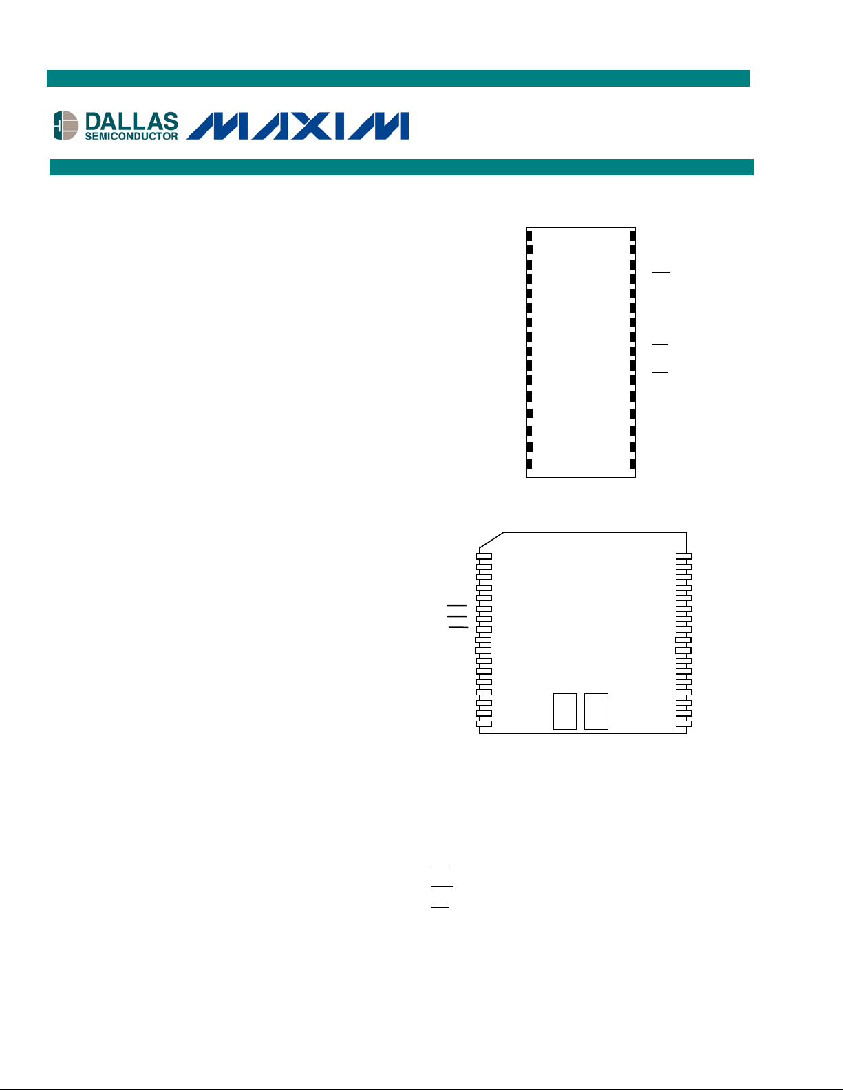
13 1 2 3 4 5 6 7 8
9
10
11
12
14
31
32-Pin Encapsulated Package
A14
A7
A5
A4
A3
A2
A1
A0
DQ1
DQ0
V
A15
NC
WE
A13
A8
A9
A11
OE
A10
CE
DQ7
DQ5
DQ6
32
30
29
28
27
26
25
24
23
22
21
19
20 A16
A12
A6
NC
DQ2
GND
15
16
18
17
DQ4
DQ3
1
NC
2
A15
A16
NC
WE
OE
CE
DQ7
DQ6
DQ5
DQ4
DQ3
DQ2
DQ1
DQ0
GND
4
5
6
7
8
9
10
12
13
14
15
16
17
NC
A14
33
32
31
30
29
28
26
25
23
22
20
18
A13
A12
A11
A10
A9
A8
A7
A6
A5
A4
A3
A2
A1
A0
34
NC
GND
V
34-Pin PowerCap Module (PCM)
19-5638; Rev 11/10
FEATURES
10 years minimum data r etent ion in the
absence of external power
Data is automatically pro tected during power
loss
Replaces 128k x 8 volatile stat ic RAM,
EEPROM or Flash memory
Unlimited write c ycles
Low-power CMOS
Read and write access t imes of 70 ns
Lithium energy sour ce is electrically
disconnected to ret ain freshness u nt il power is
applied for the first time
Full ±10% VCC operating range (DS1245Y)
Optional ±5% VCC operating range
(DS1245AB)
Optional industrial temperature range of
-40°C to +85°C, designated IND
JEDEC standard 32-pin DIP package
PowerCap Module (PCM) package
- Directly surface-mountable module
- Replaceable snap-on PowerCap provides
lithium backup battery
- Standard ized pinout for all nonvo lat ile
SRAM products
- Detachment featur e on PowerCap allows
easy removal using a regu lar screwdriver
PIN ASSIGNMENT
VCC
740-mil Extended
3
11
BAT
27
24
21
19
(Uses DS9034PC+ or DS9034PCI+ PowerCap)
PIN DESCRIPTION
A0 - A16 - Address Inputs
DQ0 - DQ7 - Data In/Dat a Out
- Chip Enable
- Write Enable
- Output Enable
VCC - Power (+5V)
GND - Ground
NC - No Co nnect
1 of 10
Page 2

DS1245Y/AB
2 of 10
CE
WE
WE
DESCRIPTION
The DS1245 1024k Nonvolatile SRAMs are1,048,576-bit, fully static, non volatile SRAMs o rganized as
131,072 words by 8 bits. Each complete NV SRAM has a self-contained lithium energy source and
control cir c uit ry wh ich c on stantly mon ito rs VCC for an o ut -of-toler a nc e c o ndit ion. W he n su c h a c o ndit io n
occurs, the lithium energy source is automatically switched on and write protection is unconditionally
enabled to pr event dat a corru ption. DIP-package DS1245 devices can be used in place of existing 128k x
8 static RAMs directly confor ming to the popular bytewide 32-p in DIP standard. DS1245 de vices in th e
PowerCap Module package are direct ly surface mountable and are normally paired with a DS9034PC
PowerCap to form a complete Nonvolatile SRAM module. There is no limit on the number of write
cycles that can be executed and no additional support circuitr y is requ ired for micro pr ocessor interfacing.
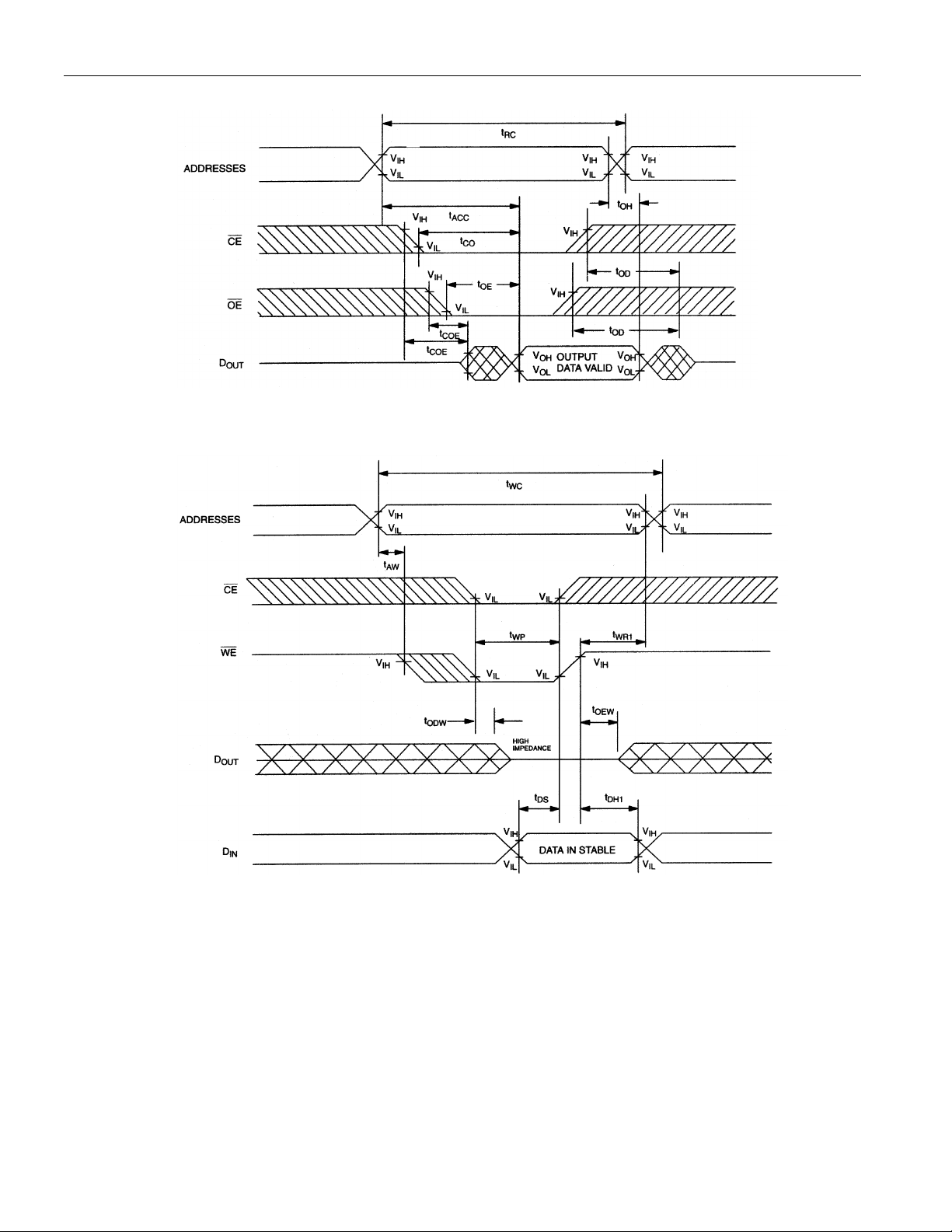
READ MODE
The DS1245 execut es a read cycle whenever WE (Writ e Enable) is inactive (high) and CE (Chip Enable)
and OE (Out put Enable) are active (low). The unique address specified by the 17 address inputs (A0 A16) defines which of the 131,072 bytes of data is to be accessed. Valid data will be available t o the eight
data output drivers within t
(Access Time) a fter the last add ress input signal is st able, providing t hat
ACC
and OE (Outp ut Enable) acces s t imes are a lso sat isfied . If OE and CE access times are not satisfied,
then data acces s must be measured fro m the lat er occurring signal (CE or OE) and the li miting parameter
is either tCO for CE or tOE for OE rather than address access.
WRITE MODE
The DS1245 executes a write cycle whenever the WE and CE signals are active (low) after address
inputs are stable. The later occurring falling edge of CE or WE will determine the st ar t of the write cycle.
The write cycle is terminated by the ear lier rising edge o f CE or
. All address inputs must be kept
valid throughout the write c ycle. WE must return to the high stat e for a minimum reco very time (tWR)
before anot her cycle can be initiat ed. The OE control signal should be kept inactive (high) during write
cycles to avoid bus contentio n. Ho w ever , if the o ut put dr ivers ar e e nab led (CE and OE a ct ive) t hen
wil l disable the o utputs in t
from its falling edge.
ODW
DATA RETENTION MODE
The DS1245AB provides full functional c ap ab ilit y for VCC greater than 4.75 volts and write protects by
4.5 volts. The DS1245Y provides full functional capability for VCC greater than 4.5 volts and writeprotects by 4.25 volts. Data is maintained in the a bsence of VCC without a n y a dd ition al support circuitry.
The nonvolatile stat ic RAMs constantly monitor VCC. Should the supply vo ltage decay, the NV SRAMs
automatically write-protect themselves, all inputs become “don’t care,” and all outputs become high
impedance. As VCC falls below approximate ly 3.0 vo lts, a power switching c ircuit connects the lit hium
energy source to RAM to r etain data. During power-up , whe n VCC rises above approximately 3.0 volts,
the power sw itching c ircuit connect s external VCC to RAM and disconnects the lithium energy source.
Normal RAM operat ion can resu me after VCC exceeds 4.75 volts for the DS1245AB and 4.5 volts for the
DS1245Y.
FRESHNESS SEAL
Each DS1245 device is shipped from Maxim with its lit hium energy source disco nnected, guaranteeing
full energy capacity. When VCC is first applied at a level greater than 4.25 vo lts, the lit hiu m e nergy source
is enabled for batt ery back-up operation.
Page 3

DS1245Y/AB
3 of 10
PACKAGES
The DS1245 devices are available in two packages: 32-pin DI P and 3 4-pin PowerCap Module (PCM).
The 3 2-p in DI P int egr at es a lit h iu m bat t er y, an S R AM memo r y and a no n vo lat ile c o ntr o l func t ion int o a
single package with a JEDEC-standard 600-mil DIP pino ut. The 34-pin PowerCap Module integrates
SRAM memo ry and nonvo lat ile cont ro l along w ith co nta cts fo r co nnection to the lithium battery in the
DS9034PC PowerCap. The PowerCap Module package design allows a DS1245 PCM device to be
surface mounted without subjecting its lithium backup battery to destructive high-temperature reflow
soldering. After a DS1245 PCM is reflow soldered, a DS9034PC PowerCap is snapped on top of the
PCM to form a complete Nonvolatile SRAM module. The DS9034PC is keyed to prevent improper
attachment. DS1245 PowerCap Modules and DS9034PC PowerCaps are ordered separately and shipped
in separate containers. See t he DS90 34P C dat a sheet for further information.
Page 4
DS1245Y/AB
4 of 10
ABSOLUTE MAXIMUM RATINGS
Voltage on Any Pin Relative to Ground -0.3V to +6.0V
Operating Temperat ur e Range
Commercial: 0°C to +70°C
Industrial: -40°C to +85°C
Storage Temperatu r e Range
EDIP -40°C to +85°C
Power Cap -55°C to +125°C
Lead Temperature (soldering, 10s) +260°C
Soldering Temperature (reflow, PowerCap) +260°C
Note: EDIP is wave or hand so ldered only.
This is a stress rating only and functional operation of the device at these or any other conditions above those indicated in the operation
sections of this specification is not implied. Exposure to absolute maximum rating conditions for extended periods of time may affect
reliability.
RECOMMENDED DC OPERATING CONDITIONS (TA: See Note 10)
PARAMETER SYMBOL MIN TYP MAX UNITS NOTES
DS1245AB Power Supply Voltage V
CC
4.75 5.0 5.25 V
DS1245Y Power Supply Voltage VCC 4.5 5.0 5.5 V
Log ic 1 VIH 2.2 VCC V
Log ic 0 VIL 0.0 0.8 V
DC ELECTRICAL CHARACTERISTICS (V
(T
PARAMETER SYMBOL MIN TYP MAX UNITS NOTES
Input Leakage Current I
I/O Leakage Current CE ≥ VIH ≤ V
Output Current @ 2.4V I
Output Current @ 0.4V I
Standby Current CE=2.2V
Standby Current CE=VCC-0.5V
Operating Current I
Write Protection Voltage (DS1245AB) V
Write Protection Voltage (DS1245Y) V
CC
: See Note 10) (VCC = 5V ±10% for DS1245Y)
A
IL
I
IO
OH
OL
I
CCS1
I
CCS2
CCO1
TP
TP
-1.0 +1.0
-1.0 +1.0
-1.0 mA
2.0 mA
200 600
50 150
85 mA
4.50 4.62 4.75 V
4.25 4.37 4.5 V
= 5V ±5% for DS1245AB)
CC
µA
µA
µA
µA
CAPACITANCE (T
= +25°C)
A
PARAMETER SYMBOL MIN TYP MAX UNITS NOTES
Input Capacitance C
Input/ Output Capacitance C
IN
I/O
5 10 pF
5 10 pF
Page 5

DS1245Y/AB
5 of 10
OE
CE
OE
WE
AC ELECTRICAL CHARACTERISTICS (VCC = 5V ±5% for DS1245AB)
(T
: See Note 10) (VCC = 5V ±10% for DS1245Y)
A
PARAMETER SYMBOL
Read Cycle Time t
Acce ss T ime t
to Outp ut Valid
to Outp ut Valid
or CE to Outp ut Acti ve
Out put High Z fr om Deselection t
Output Hold from Address Change t
Writ e Cycle Time t
Write Pulse Width t
Address Setup Time t
Write Recovery Time
Out put High Z fr om
RC
ACC
t
OE
t
CO
t
COE
OD
OH
WC
WP
AW
t
WR1
t
WR2
t
ODW
DS1245AB-70
DS1245Y-70
UNITS NOTES
MIN MAX
70 ns
70 ns
35 ns
70 ns
5 ns 5
25 ns 5
5 ns
70 ns
55 ns 3
0 ns
5
15
ns
ns
25 ns 5
12
13
Output Active from WE
Data Setup Time t
Data Hold Time
t
OEW
DS
t
DH1
t
DH2
5 ns 5
30 ns 4
0
10
ns
ns
12
13
Page 6
6 of 10
READ CYCLE
DS1245Y/AB
SEE NOTE 1
WRITE CYCLE 1
SEE NOTES 2, 3, 4, 6, 7, 8, and 12
Page 7
7 of 10
WRITE CYCLE 2
DS1245Y/AB
SEE NOTES 2, 3, 4, 6, 7, 8, and 13
POWER-DOWN/POWER-UP CONDITION
Page 8

DS1245Y/AB
8 of 10
WE
WE
WE
OE
WE
WE
WE
WE
WE
WE
POWER-DOWN/POWER-UP TIMING (TA: See Note 10)
PARAMETER SYMBOL MIN TYP MAX UNITS NOTES
VCC Fail Detect to CE and
Inactive
VCC s lew fr om VTP to 0V t
VCC slew from 0V to VTP t
VCC Va lid to CE and
Inactive
VCC Valid to End of Write Protection t
t
PD
F
R
t
PU
REC
1.5
150
150
µs
µs
µs
2 ms
125 ms
11
(T
PARAMETER SYMBOL MIN TYP MAX UNITS NOTES
Expected Dat a Retent ion T ime t
DR
10 years 9
= +25°C)
A
WARNING:
Under no circumstance are negative undershoots, of any amplitude, allowed when device is in batter y
backup mode.
NOTES:
1.
2.
3. tWP is specified as the logical AND o f CE and
4. tDH, tDS are measured from the earlier o f CE or
5. These parameters ar e sa mpled with a 5 pF load and ar e not 100% t ested .
6. If t h e CE low trans it ion o ccur s si mult aneo us ly wit h o r lat ter than t he
7. If t he CE high transition occurs prior to or simultaneously with the
8. If
9. Each DS1245 has a built-in switch that disco nnects t he lithium sou rce unt il the user first ap plies VCC.
10. Each DS1245 has a built-in sw itch tha t d isconnec t s the lit h iu m so u r ce until VCC is first applied by the
11. All AC and DC electrical characteristics are valid over the full operating temperature range. For
12. In a power-down condition the volt age on any p in may not e xc eed the voltage on VCC.
is high for a Read Cycle.
= VIH or VIL. If OE = VIH during write cycle, t he o ut put buffers remain in a high impedance state.
. tWP is measured from the latter of CE or
going low to the earlier of CE or WE going h igh.
going h ig h.
lo w t r an sit io n, t he o ut put
buffers remain in a high impedance state during this period.
high transit ion, the out put
buffe r s r e main in high imped a nc e st a t e dur ing this period.
is low or the WE low t r a ns ition o cc u r s p r io r t o or s im u lt a ne o u s l y w it h t he CE low t r a ns ition ,
the output buffers remain in a high impedance state during this period.
The expected tDR is defined as accu mulative t ime in the absence o f VCC starting from the t ime power
is first app lied by the user. T his paramet er is ass ured by component selection, pr ocess control, and
design. It is not measured directly during production testing.
user. The e xpected tDR is defined as acc umu lat ive t ime in the abs ence o f VCC sta rting fro m t he t ime
power is first applied by the user.
comme rc ia l pro d uct s, t his r ang e is 0°C t o 70°C. For industrial products (IND), this range is -40°C to
+85°C.
Page 9

9 of 10
13. t
WE
SUPPLY
TOLERANCE
SPEED GRADE
(ns)
DS1245AB-70+
0°C to +70°C
5V ± 5%
32 740 EDIP
70
DS1245ABP-70+
0°C to +70°C
5V ± 5%
34 PowerCap*
70
DS1245AB-70IND+
-40°C to +85°C
5V ± 5%
32 740 EDIP
70
DS1245ABP-70IND+
-40°C to +85°C
5V ± 5%
34 PowerCap*
70
DS1245Y-70+
0°C to +70°C
5V ± 10%
32 740 EDIP
70
DS1245YP-70+
0°C to +70°C
5V ± 10%
34 PowerCap*
70
DS1245Y-70IND+
-40°C to +85°C
5V ± 10%
32 740 EDIP
70
DS1245YP-70IND+
-40°C to +85°C
5V ± 10%
34 PowerCap*
70
14. t
WR1
WR2
and t
and t
are measured from
DH1
are measured from CE going h ig h.
DH2
going h ig h.
15. DS1245 modules are recognized by Underwriters Laboratories (UL) under file E99151.
DC TEST CONDITIONS AC TEST CONDITIONS
Outputs Open Output Load: 100 pF + 1TTL Gate
Cycle = 200 ns for operating current Input Pulse Levels: 0 - 3.0V
All voltages are refere nced to grou nd Timing Measurement Reference Levels
Input: 1.5V
Output: 1.5V
Input pulse Rise and Fall Times: 5 ns
ORDERING INFORMATION
DS1245Y/AB
PART TEMP RANGE
+Denotes a lead(Pb)-free/RoHS-compliant package.
*DS9034PC+ or DS9034PCI+ (PowerCap) required. Must be ordered separate ly.
PIN-PACKAGE
PACKAGE INFORMATION
For the latest package outline information and land patterns, go to www.maxim-ic.com/packages. Note that a “+”,
“#”, or “-” in the package code indicates RoHS status only. Package drawings may show a different suffix
character, but the drawing per tains to the p ackage re gard less of RoHS status.
PACKAGE TYPE PACKAGE CODE OUTLINE NO. LAND PATTERN NO.
32 EDIP MDT32+6
34 PCAP PC2+3
21-0245
21-0246
—
—
 Loading...