

Page 1
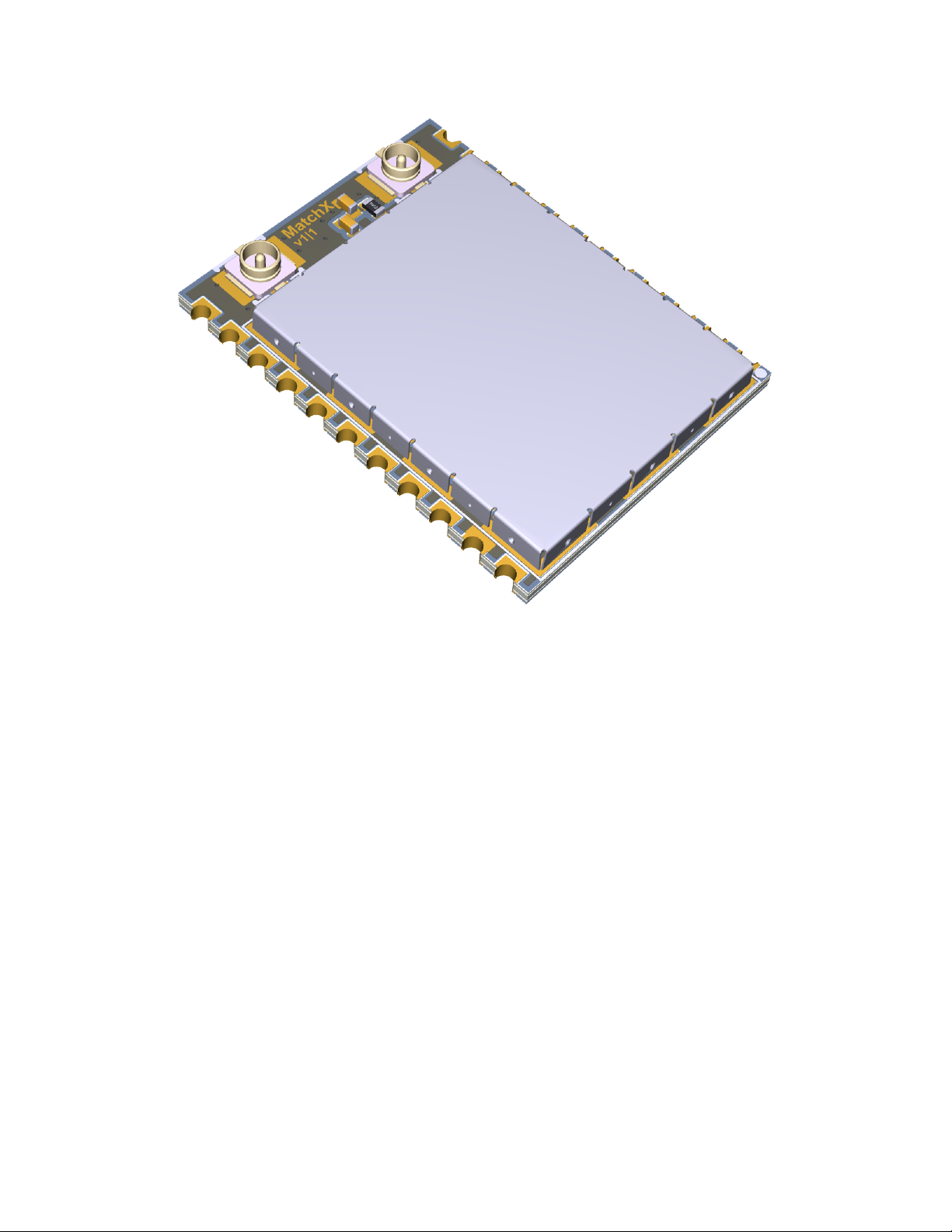
MatchX MX1731 Core
BLE and LoRa enabled System on Module
(Preliminary)
User Guide
V1.0
Page 2

Copyrightc 2017 MatchX GmbH
WW W.MATC HX .I O
No part of the specifications may be reproduced in any form or by any means or used to make any
derivative such as translation, transformation, or adaptation without permission from MatchX GmbH
All rights reserved.
First release, Nov 2017
Page 3
Contents
1 Introduction . . . . . . . . . . . . . . . . . . . . . . . . . . . . . . . . . . . . . . . . . . . . . . . . . . . . 5
1.1 Product overview . . . . . . . . . . . . . . . . . . . . . . . . . . . . . . . . . . . . . . . . . . . . . . . . 5
1.1.1 Lora . . . . . . . . . . . . . . . . . . . . . . . . . . . . . . . . . . . . . . . . . . . . . . . . . . . . . . . . . . . . 5
1.1.2 BLE . . . . . . . . . . . . . . . . . . . . . . . . . . . . . . . . . . . . . . . . . . . . . . . . . . . . . . . . . . . . . 6
1.2 Main Features . . . . . . . . . . . . . . . . . . . . . . . . . . . . . . . . . . . . . . . . . . . . . . . . . . . 6
1.2.1 Hardware . . . . . . . . . . . . . . . . . . . . . . . . . . . . . . . . . . . . . . . . . . . . . . . . . . . . . . . . 6
1.2.2 Software . . . . . . . . . . . . . . . . . . . . . . . . . . . . . . . . . . . . . . . . . . . . . . . . . . . . . . . . . 6
2 Hardware Architecture - SoM module . . . . . . . . . . . . . . . . . . . . . . . . . . . . 7
2.1 Pin-out and pin description of the SoM module . . . . . . . . . . . . . . . . . . . . . . . 7
2.2 Operating frequency bands . . . . . . . . . . . . . . . . . . . . . . . . . . . . . . . . . . . . . . . 9
2.2.1 EU 863-870MHz ISM Band . . . . . . . . . . . . . . . . . . . . . . . . . . . . . . . . . . . . . . . . . . . . 9
2.2.2 US 902-928MHz ISM Band . . . . . . . . . . . . . . . . . . . . . . . . . . . . . . . . . . . . . . . . . . . . 9
2.2.3 Australia 915-928MHz ISM Band . . . . . . . . . . . . . . . . . . . . . . . . . . . . . . . . . . . . . . 11
2.3 Connection . . . . . . . . . . . . . . . . . . . . . . . . . . . . . . . . . . . . . . . . . . . . . . . . . . . . 11
2.3.1 Power . . . . . . . . . . . . . . . . . . . . . . . . . . . . . . . . . . . . . . . . . . . . . . . . . . . . . . . . . . 11
2.3.2 Bluetooth connection . . . . . . . . . . . . . . . . . . . . . . . . . . . . . . . . . . . . . . . . . . . . . 12
3 Connecting to MatchX server . . . . . . . . . . . . . . . . . . . . . . . . . . . . . . . . . . 13
3.1 Registering a node on MarchX server . . . . . . . . . . . . . . . . . . . . . . . . . . . . . . 13
4 Software Development Guide . . . . . . . . . . . . . . . . . . . . . . . . . . . . . . . . . . 15
4.1 References . . . . . . . . . . . . . . . . . . . . . . . . . . . . . . . . . . . . . . . . . . . . . . . . . . . . . 15
Page 4

4
4.2 Prerequisites . . . . . . . . . . . . . . . . . . . . . . . . . . . . . . . . . . . . . . . . . . . . . . . . . . . . 15
4.3 Software development under Windows OS . . . . . . . . . . . . . . . . . . . . . . . . . . 16
4.3.1 Using SmartSnippet Studio . . . . . . . . . . . . . . . . . . . . . . . . . . . . . . . . . . . . . . . . . . 18
4.4 Software development under Linux . . . . . . . . . . . . . . . . . . . . . . . . . . . . . . . . 20
4.5 Setting DevEUI, AppEUI and DevKey . . . . . . . . . . . . . . . . . . . . . . . . . . . . . . . 21
5 Typical Hardware Connection . . . . . . . . . . . . . . . . . . . . . . . . . . . . . . . . . . 24
5.1 Digital Interfaces . . . . . . . . . . . . . . . . . . . . . . . . . . . . . . . . . . . . . . . . . . . . . . . . 25
5.2 Analog Interfaces . . . . . . . . . . . . . . . . . . . . . . . . . . . . . . . . . . . . . . . . . . . . . . . 25
5.3 Programming Interface . . . . . . . . . . . . . . . . . . . . . . . . . . . . . . . . . . . . . . . . . . 25
5.4 Antenna connection . . . . . . . . . . . . . . . . . . . . . . . . . . . . . . . . . . . . . . . . . . . . 25
6 Product specification . . . . . . . . . . . . . . . . . . . . . . . . . . . . . . . . . . . . . . . . . . 28
6.1 Hardware environment . . . . . . . . . . . . . . . . . . . . . . . . . . . . . . . . . . . . . . . . . . 28
6.2 Software environment . . . . . . . . . . . . . . . . . . . . . . . . . . . . . . . . . . . . . . . . . . . 28
6.3 RF performance . . . . . . . . . . . . . . . . . . . . . . . . . . . . . . . . . . . . . . . . . . . . . . . . . 29
6.4 Electrical characteristics . . . . . . . . . . . . . . . . . . . . . . . . . . . . . . . . . . . . . . . . . 29
6.5 Antenna characteristics . . . . . . . . . . . . . . . . . . . . . . . . . . . . . . . . . . . . . . . . . . 29
6.6 Dimensions . . . . . . . . . . . . . . . . . . . . . . . . . . . . . . . . . . . . . . . . . . . . . . . . . . . . . 30
7 Certification . . . . . . . . . . . . . . . . . . . . . . . . . . . . . . . . . . . . . . . . . . . . . . . . . . . 32
7.1 FCC . . . . . . . . . . . . . . . . . . . . . . . . . . . . . . . . . . . . . . . . . . . . . . . . . . . . . . . . . . . 32
7.1.1 Antenna information . . . . . . . . . . . . . . . . . . . . . . . . . . . . . . . . . . . . . . . . . . . . . . 34
7.2 CE . . . . . . . . . . . . . . . . . . . . . . . . . . . . . . . . . . . . . . . . . . . . . . . . . . . . . . . . . . . . 34
8 Important Notice . . . . . . . . . . . . . . . . . . . . . . . . . . . . . . . . . . . . . . . . . . . . . . 35
Page 5
1. Introduction
1.1 Product overview
The LPWAN Core module by MatchX is a high performance, ready to use system on module
allowing you to kick-start your IoT project. It is an incredibly flexible solution that can be deployed
in a various number of applications which require long distance communication and long battery
life. The unique combination of both LoRa and Bluetooth Low Energy makes non-contact firmware
updates easy, especially when the device is mounted in a difficult or unaccessible place.
This guide covers both the US and EU version of the Core module. The main differences between
these two versions are listed in Table 1.1.
Parameter US EU
Operating Frequency Band 902-928MHz 863-870MHz
Maximum Output Power +17dBm +14dBm
Lora BW 500k/125kHz 125kHz
SF 7-10 7-12
Certification IEC 60950-1 EN 300200
FCC PART 15.247 EN 301489
1.1.1 Lora
The MatchX Module uses LoRa communication to send messages over long distances (up to 20km
in open spaces). This unique modulation scheme guarantees robust wireless communication even in
difficult from RF point of view environments such as high-rise city landscapes or within the inside
of buildings. The module can output up to 18dBm of power and is fully LoraWAN compatible. It’s
uniquely designed to work with the MatchX Box gateway and can also be used with a LoraWAN
compatible Gateway of your choice.
Table 1.1: Comparison of different regions
Page 6

6 Chapter 1. Introduction
1.1.2 BLE
The module offers a novel firmware solution upgrade by augmenting LoRa, together with Bluetooth
Low Energy (BLE). As LoRa protocol is not suitable for transmitting large amounts of data, MatchX
has combated this with BLE, offering a quick, robust and remote way of updating your software.
It is a perfect method in cases where a sensor may be mounted in an unaccessible place like in a
basement, sealed container box or behind a wall. Moreover BLE together with provided mobile app
enables you to configure your module and read its status and additional data.
1.2 Main Features
Long range, long battery life, flexible sensor configuration and wireless firmware update are the key
features that are offered by the Core module.
1.2.1 Hardware
• +18dBm output power in 868MHz
• -146dBm sensitivity of LoraWAN packets
• integrated LoRa and BLE antennas connectors
• 0 Hz up to 96 MHz 32-bit ARM Cortex-M0 microcontroller
• Dialog DA14680
• Semtech SX1276
• Li-ION battery charger
• ultra low power design
1.2.2 Software
• Runs LoRa and Bluetooth stack simultaneously
• Bluetooth low energy (Bluetooth 4.2 specification)
• Low power consumption modes
• Easy to use software package
• Eclipse-based IDE
• Firmware upgrade over the air
• Mobile application
Currently there is no Class B support in server yet, but the hardware and firmware are fully
R
prepared for Class B specification, it is expected to support Class B in future firmware upgrade.
Page 7
2. Hardware Architecture - SoM module
2.1 Pin-out and pin description of the SoM module
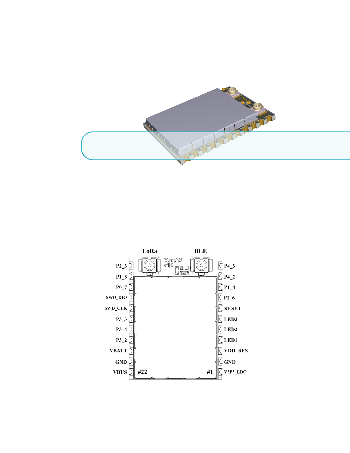
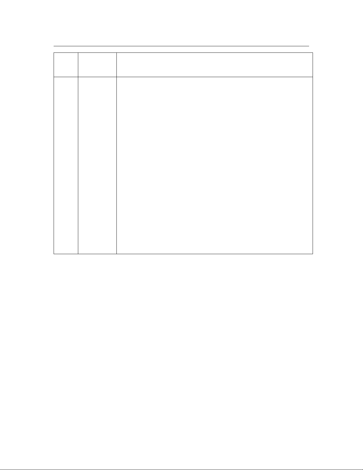
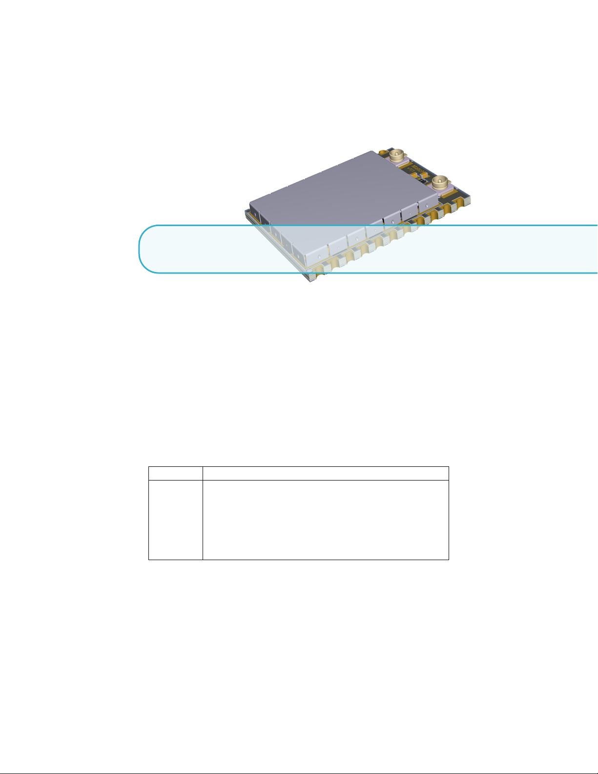
The pin-out of the MatchX Core SoM module can be seen on Figure 2.1 and the description of the
pins in Table 2.1. On top of the module there are two UF.L RF connectors, the one on the left is the
LoRa antenna connector, a suitable 868MHz in EU and 915MHz in US, 50 Ohm antenna is expected
to be connected on these port. The other connector is for connecting the 2.4GHz, 50 Ohm BLE
antenna. Please contact MatchX for antenna recommendation.
Figure 2.1: Pin-out of the SoM module.
Page 8
8 Chapter 2. Hardware Architecture - SoM module
Pin
number
1 V3P3_LDO 3.3V output of the internal LDO
2 GND Ground
3 VDD_RFS Supply voltage of the radio front-end
4 LED1 Open drain output type, LED driver
5 LED2 Open drain output type, LED driver
6 LED3 Open drain output type, LED driver
7 RESET Reset signal, active high
8 P1_6 General Purpose I/O P1_6 / NTC resistor for battery temperature sensing
9 P1_4 General Purpose I/O P1_4 / ADC1 / battery temperature sensing
10 P4_2 General Purpose I/O P4_2
11 P4_3 General Purpose I/O P4_3
12 P2_3 General Purpose I/O P2_3
13 P1_3 General Purpose I/O P1_3 / ADC2
14 P0_7 General Purpose I/O P0_7 / ADC3
15 SWD_DIO Serial Wire Debug interface I/O signal / GPIO P0_6 / ADC4
16 SWD_CLK Serial Wire Debug interface clock signal / GPIO P2_4 / ADC7
17 P3_3 General Purpose I/O P3_3
18 P3_4 General Purpose I/O P3_4
19 P3_2 General Purpose I/O P3_2
20 VBATT Battery voltage input
21 GND Ground
22 VBUS 5V supply, charging voltage
Name Description
Table 2.1: USB-C connector pins description.
The module can be powered in two ways:
1. By connecting the VBATT to a battery voltage (2.7V to 4.2V).
2. By supplying +5V on the VBUS pin.
If both power sources are present, the battery will be charged form +5V power supply. The charging
current and charging characteristics for different battery types is software configurable. The module
provides
used to supply external devices, but the maximum current drawn can’t be grater than 100mA. By
default
VDD_RFS
with +17dBm power. This has to be taken in consideration when planning the power budget of
V3P3_LDO
power source for
low power converter.
LDO, when
battery voltage. By default all GPIO are referenced to
1.8V as the GPIO level, each GPIO can be configured individually) so care must be taken to ensure
V3P3_LDO
VDD_RFS
is around 35mA during transmission with +14dBm power output and around 90mA
. When even higher RF transmission power is required it is advisable to use different
The source of
VBUS
voltage, it is a output of internal LDO of the DA14680 MCU, and it can be
is connected to
VDD_RFS
V3P3_LDOisVBUS
is not present, and
V3P3_LDO
. On the Evaluation Board it can be done by using 3.3V output of the
when present or
VBATT
with an external 0R resistor. The current draw of
VBATT
drops below 3.3V the
V3P3_LDO
otherwise. As it is a output of a
V3P3_LDO
(it is also possible to configure
will follow the
Page 9
2.2 Operating frequency bands 9
that no voltage higher than
external devices, that connect to SoM module, from a boost converter.
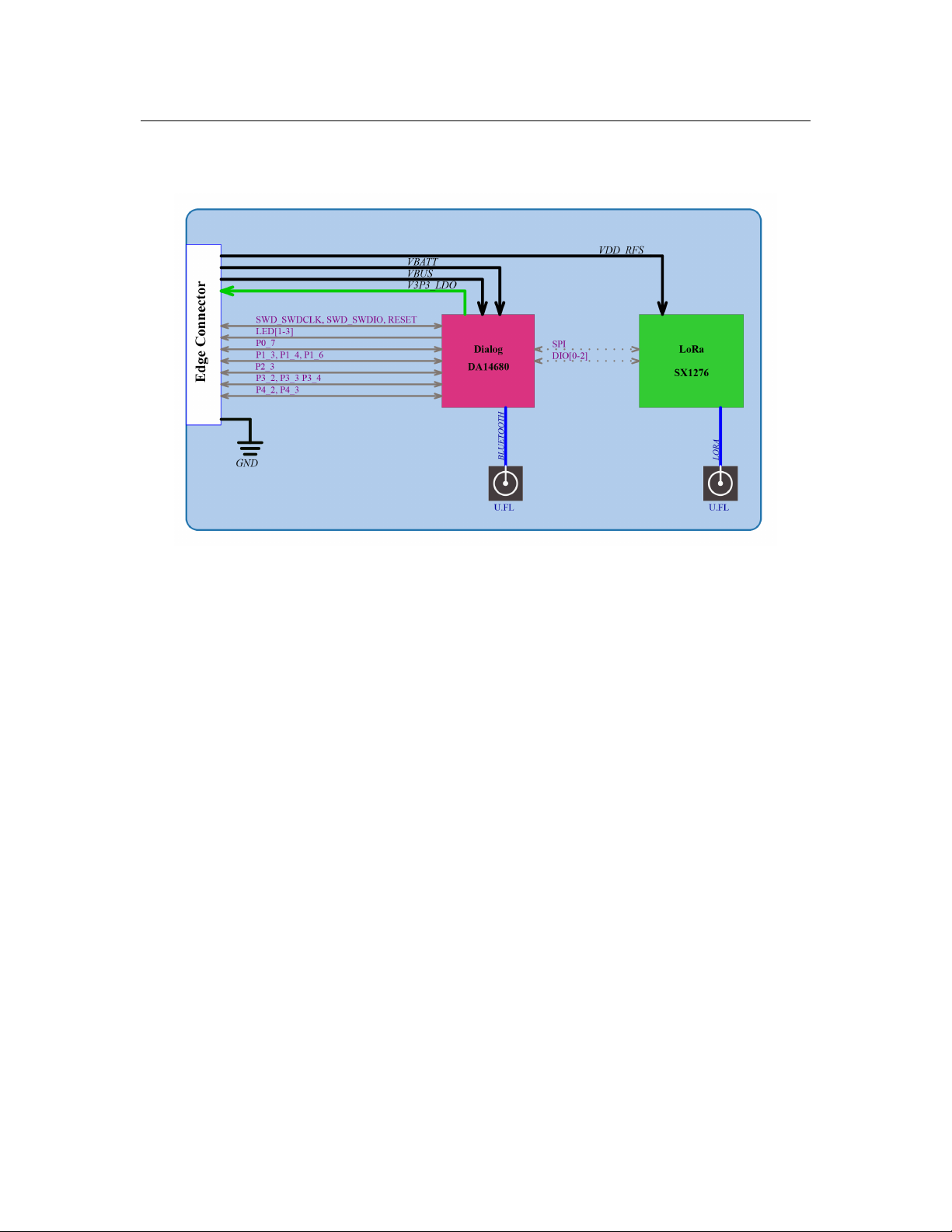
Figure 2.2: Block diagram of the Core module.
V3P3_LDO
is presented to any GPIO. This may happen when powering
2.2 Operating frequency bands
2.2.1 EU 863-870MHz ISM Band
In the European region the EN300220-2 V3.1.1 (2017-02) regulation defines the allowed frequency
allocation and spectrum access. Every device working in this band must comply with these rules
as shown in the Table 2.3. EU regulations restrict the maximum radiated power as well as the duty
cycle of the transmission in different frequency bands.To comply with the duty cycle requirement the
transmitting device must wait after every transmitted packet. The time device has to wait depends
on the time on air of transmitted packet and this in turn depends on the length of the packet and
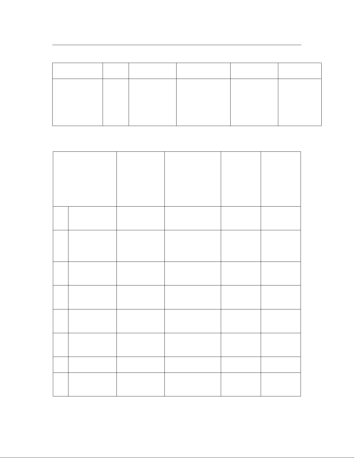
spreading factor SF. This relation and required wait time can be seed in Table 2.2 According to
LoRaWAN specification every device has to implement at least 3 channels as follows:
• 868.10 MHz
• 868.30 MHz
• 868.50 MHz
The SoM is preconfigured to work with the MatchX Box gateway and additionally to the 3 mandatory
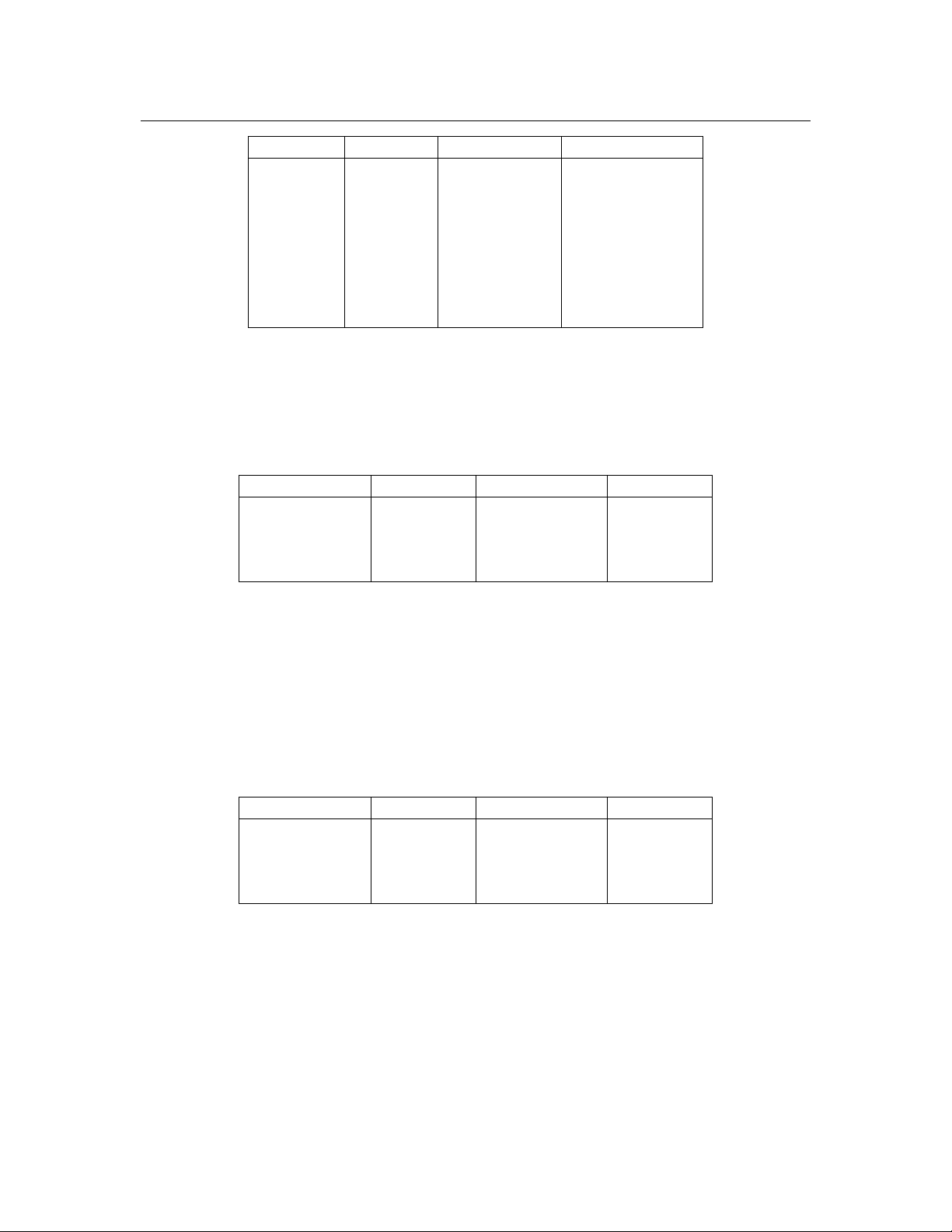
channels 5 additional channels are defined. The list of all preconfigured channels can be found in
Table 2.4.
2.2.2 US 902-928MHz ISM Band
These frequencies band can be used in USA, Canada and all other countries that adopt the entire
FCC-Part15 regulations in 902-928 ISM band. For these region MatchX uses predefined frequencies
Page 10
10 Chapter 2. Hardware Architecture - SoM module
Spreading Factor Bit rate Range (depends Time on air (ms) 0.1% duty cycle 1% duty cycle
(125kHz Lora) (bps) on conditions) (10 bytes payload) waiting time waiting time
SF7 5470 2 km 56 ms 1 min 6s
SF8 3125 4 km 100 ms 1 min 40s 10s
SF9 1760 6 km 200 ms 3 min 20s 20s
SF10 980 8 km 370 ms 6 min 10s 37s
SF11 440 14 km 740 ms 12 min 20s 1 min 14s
SF12 290 20 km 1400 ms 23 min 20s 2min 20s
Table 2.2: Modules operating frequencies.
Class 1 sub-
Operational Frequency band
863,000 MHz to
K
865,000 MHz
865,000 MHz to
L
868,000 MHz
868,000 MHz to
M
868,600 MHz
868,700 MHz to
N
869,200 MHz
869,400 MHz to
O
869,650 MHz
869,400 MHz to
P
869,650 MHz
869,700 MHz to
Q
870,000 MHz
869,700 MHz to
R
870,000 MHz
Channel access and
Maximum e.r.p
25 mW e.r.p.
25 mW e.r.p.
Power density:
-4,5 dBm/100
kHz
25 mW e.r.p.
25 mW e.r.p.
25 mW e.r.p.
500 mW e.r.p.
5 mW e.r.p. No requirement 56a 31
25 mW e.r.p.
occupation rules
(e.g. Duty cycle or
LBT + AFA)
≤
0,1% duty cycle
or polite spectrum
access
≤
1 % duty cycle or
polite spectrum access
≤
1% duty cycle or
polite spectrum access
≤
0,1% duty cycle
or polite spectrum
access
≤
0,1% duty cycle
or polite spectrum
access
≤
10 % duty cycle
or polite spectrum
access
≤
1% duty cycle or
polite spectrum access
Band number from
EC Decision
2013/752/EU
[i.3]
46a 66
47 67
48 28
50 29
54a 130
54b 30
56c 69
class number
according
Commission
Decision
2000/299/EU
[i.7]
Table 2.3: EU wide harmonized national radio interfaces.
Page 11
2.3 Connection 11
Frequency Bandwidth Maximum e.r.p Channel access
864.7 MHz 125 kHz 14 dBm ≤0,1% duty cycle
864.9 MHz 125 kHz 14 dBm ≤0,1% duty cycle
865.1 MHz 125 kHz -4.5 dBm ≤1% duty cycle
865.3 MHz 125 kHz -4.5 dBm ≤1% duty cycle
868.1 MHz 125 kHz 14 dBm ≤1% duty cycle
868.3 MHz 125 kHz 14 dBm ≤1% duty cycle
868.5 MHz 125 kHz 14 dBm ≤1% duty cycle
868.8 MHz 125 kHz 14 dBm ≤0,1% duty cycle
Table 2.4: Core Module operating frequencies in EU 863-870MHz ISM Band.
listed in Table 2.5. The FCC regulation puts restriction on the maximum dwell time of 400ms in
uplink, thats why the maximum allowed spreading factor is SF10.
Channel number Frequency Channel number Frequency
1 903.90 MHz 5 904.70 MHz
2 904.10 MHz 6 904.90 MHz
3 904.30 MHz 7 905.10 MHz
4 904.50 MHz 8 905.30 MHz
Table 2.5: Modules operating frequencies (uplink) in US 902-928MHz ISM Band.
2.2.3 Australia 915-928MHz ISM Band
These frequencies band can be used in Australia region. For these region MatchX uses predefined
frequencies listed in Table 2.6. All channels use 125kHz bandwidth and maximum of +20dBm
output power can be reached.
Channel number Frequency Channel number Frequency
1 915.20 MHz 5 916.00 MHz
2 915.40 MHz 6 916.20 MHz
3 915.60 MHz 7 916.40 MHz
4 915.80 MHz 8 916.60 MHz
Table 2.6: Modules operating frequencies (uplink) in Australia 915-928MHz ISM Band.
2.3 Connection
2.3.1 Power
The Core module can be supplied directly from rechargeable lithium battery. As long as the battery is
charged there is no other power connection required for the module to work.Alternatively the module
Page 12
12 Chapter 2. Hardware Architecture - SoM module
can be powered by +5V supply connected to VBus pin. Core SoM integrates internal Lithium battery
charger which will charge the battery connected to its VBatt pin from VBus voltage.Charger can be
disabled in software if the application doesn’t require it.
Important!
!
MatchX strongly recommends to charge the battery within specified temperature range of 0 to
+45◦C. Charging outside of these recommended conditions may lead to either reduced battery
life or permanent damage.
2.3.2 Bluetooth connection
The Core module implements Bluetooth Low Energy (Bluetooth 4.2 specification) with SUOTA
(Software Update Over The Air) feature. The only hardware requirement is a connection of 2,4GHz,
50 Ohm antenna to BLE antenna port.
Page 13
3. Connecting to MatchX server
Every Core module comes with preprogrammed unique MAC address, AppEUI and LoraWAN
DevKey (also referred as AppKey by different sources). The DevKey is used to ensure a secure
communication and data encryption between the module and application server. AppEUI is used to
communicate with the application that registered on the Lora server. Care must be taken with storing
the DevKey in a safe place and ensuring it is not compromised.
The products will come with a QR code sticker, which gives the Serial Number of the device. By
typing in the S/N at the registration of the MatchX LPWAN Cloud, the preprogrammed APP EUI,
MAC address and DevKey will be associated automatically.
3.1 Registering a node on MarchX server
Registering a node on MatchX server is a straight forward process. The user needs to know nodes
DevKey, DevEUI and AppEUI. For more information about these keys refer to section 4.5.
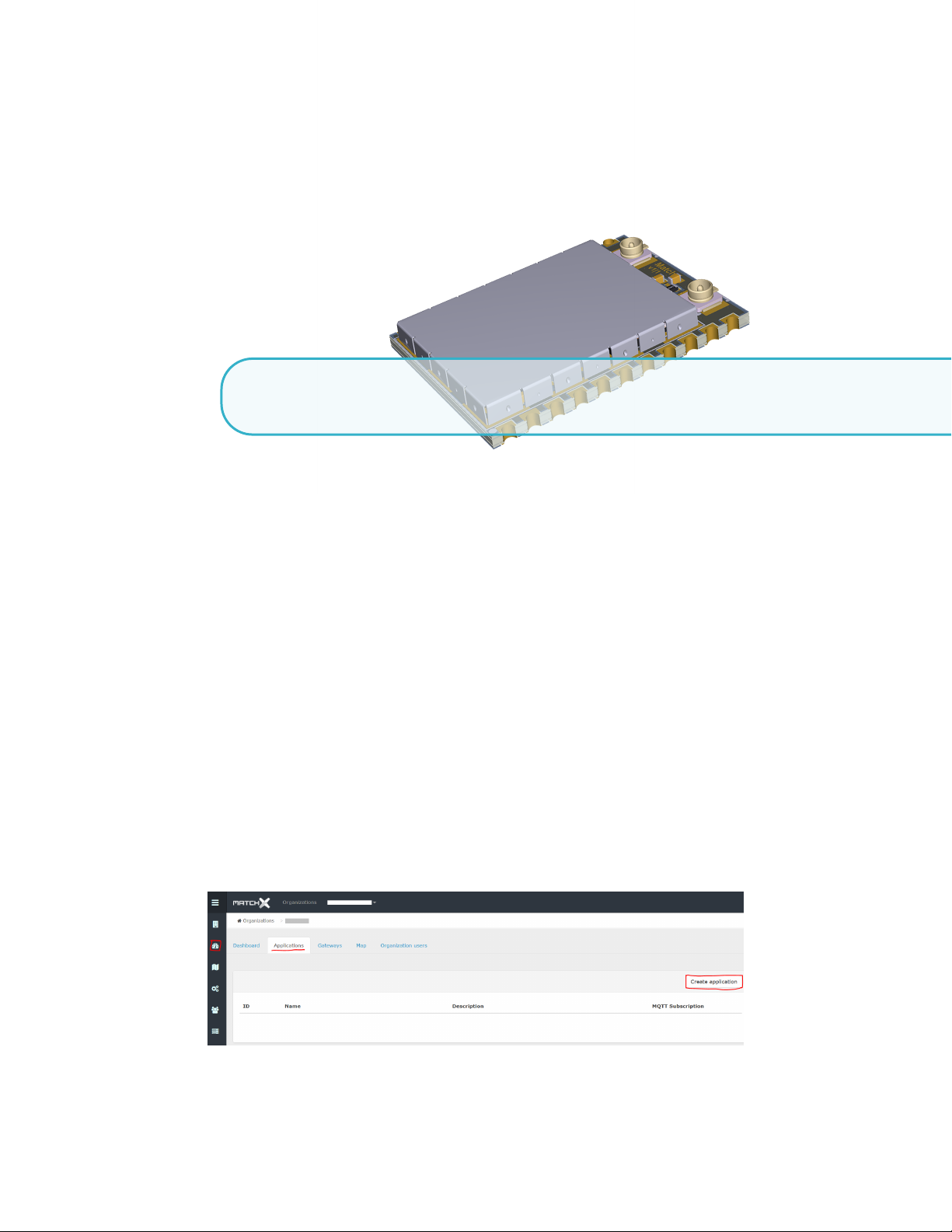
Go to matchx.io and under ’Cloud’ find an appropriate server according to region the node
should be deployed. In this example we are using https://eux.matchx.io for Europa region. Register
an account using valid email address. Go to your dashboard and click on ’Application’ tab and than
press ’Create application’ button (see Figure 3.1).
Figure 3.1: Creating new Application.
Page 14
14 Chapter 3. Connecting to MatchX server
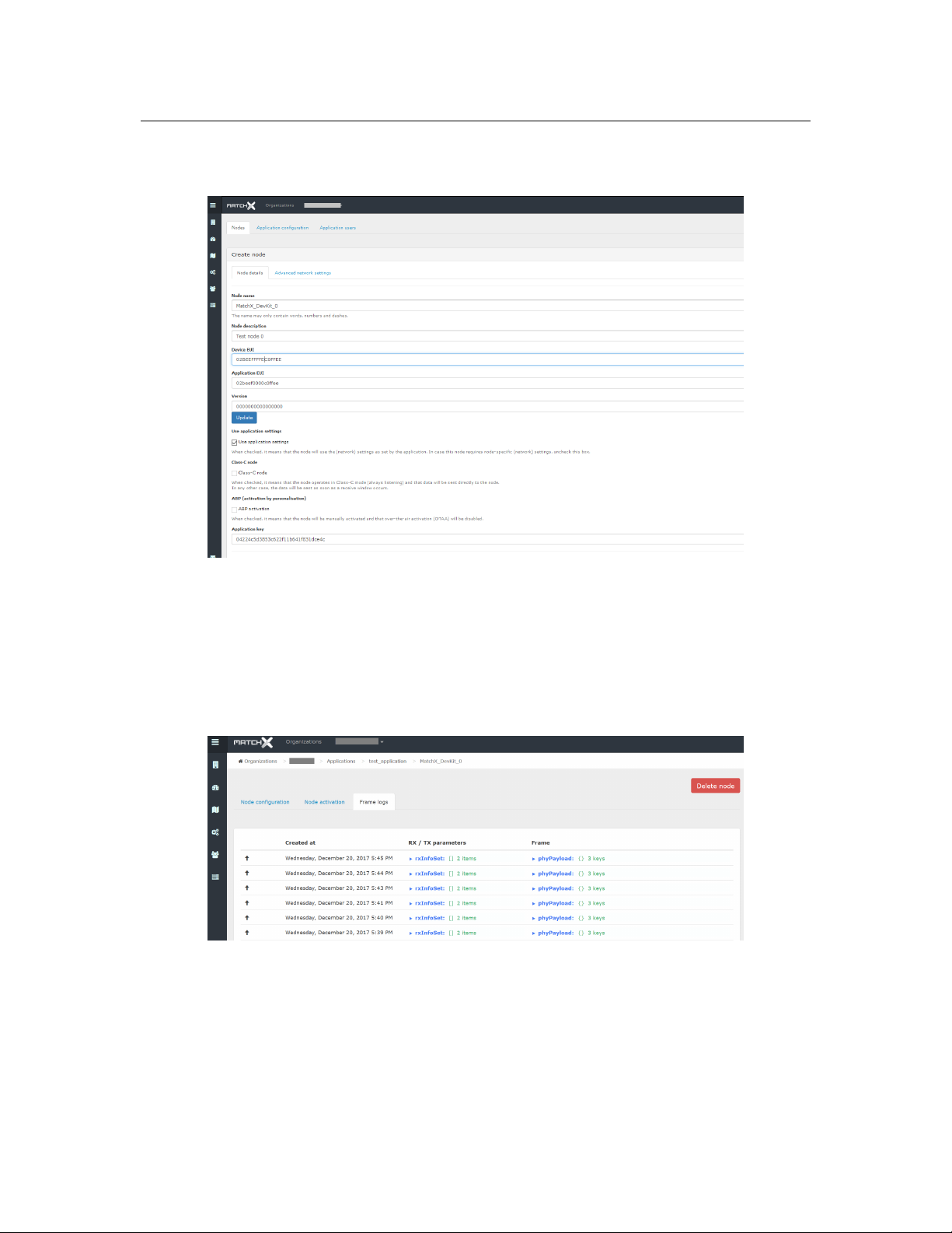
Fill out the ’Application name’ and ’Application description’ fields and click ’Submit’. Click on
your newly created application and under ’Nodes’ tab click on the ’Create node’ button.
Figure 3.2: Creating new node.
Fill out information about DevKey, DevEUI and AppEUI. Device EUI should be in 64bit format
(with fffe in the middle) like on Figure 3.2. Click on ’Submit’ button. The node is now created, you
can click on ’View’ under ’Frame Logs’ to see all messages belonging to the node like it is shown
on Figure 3.3.
Figure 3.3: Nodes messages.
Page 15
4. Software Development Guide
The purpose of this chapter is to help user to quickly install all necessary software components and
establish hardware connections needed to start software development using MarchX Core SoM and
Development Kit. MatchX is providing the Dev Kit Firmware (DKF) to be a starting point for further
software development according to individual needs.
4.1 References
SoM module is based on Dialog DA14680 microcontroller so it is advisable to get familiar with the
following documents available on Dialog Semiconductors website:
• DA14680-01 DS, Datasheet, Dialog Semiconductor
• UM-B-057-SmartSnippets Studio user guide, User manual, Dialog Semiconductor
• UM-B-047 DA1468x Getting Started, User manual, Dialog Semiconductor
• UM-B-044 DA1468x Software Platform Reference, User manual, Dialog Semiconductor
• UM-B-056 DA1468x Software Developer’s Guide, Dialog Semiconductor
4.2 Prerequisites
• MatchX Development Kit
• USB-C cable and 5V charger
• UART-USB converter
• JLink programmer
• Dialog’s Semiconductor SmartSnippets DA1468x SDK
• SmartSnippets Studio package
• MatchX Dev Kit Firmware
• Operating System (Windows or Linux)
Page 16
16 Chapter 4. Software Development Guide
4.3 Software development under Windows OS
The easiest way to install and configure all required tools is to install Dialogs SmartSnippets Studio
package (it can be downloaded from the company website after registration). Experienced users can
try to install all cross-compilation tools and configure they favorite SDE manually, but using Dialogs
software the whole process is straight forward. Please follow UM-B-057 User Manual from Dialog
for details about the installation.
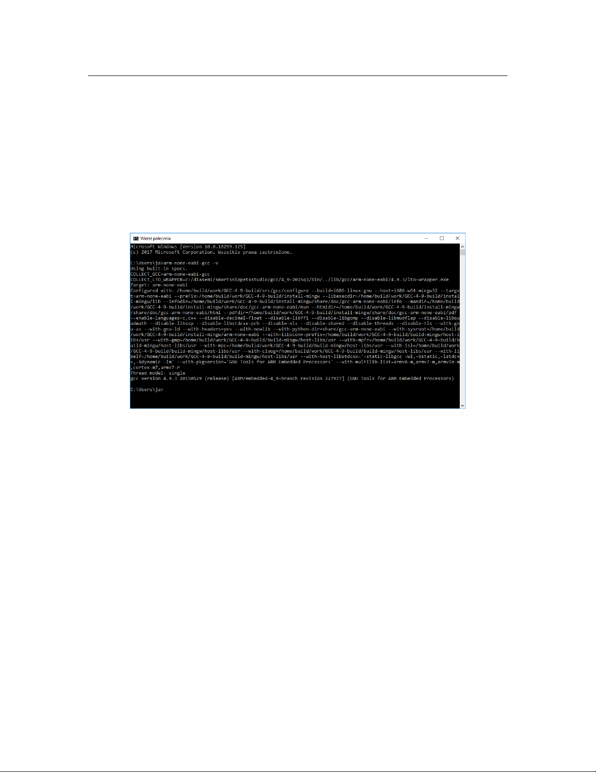
After successful installation of SmartSnippets Studio and J-Link programmer, you should
have gcc cross-compilation tools installed and proper PATH entry should exist, to check it you can
open command line window and type
to what is shown on Figure 4.1. In these example we are using gcc version 4.9.3 20150529.
arm-none-eabi-gcc -v
The result should be similar
Figure 4.1: Checking ARM tools installation.
Download the Dialog’s Semiconductor SmartSnippets DA1468x SDK (in the example the SDK
version 1.0.8.1050.1 has been used) and MatchX Dev Kit Frmware. Both SDK and Dev Kit Firmware
should be put in one folder (for example SmartSnippet workspace folder). DKF folder contains
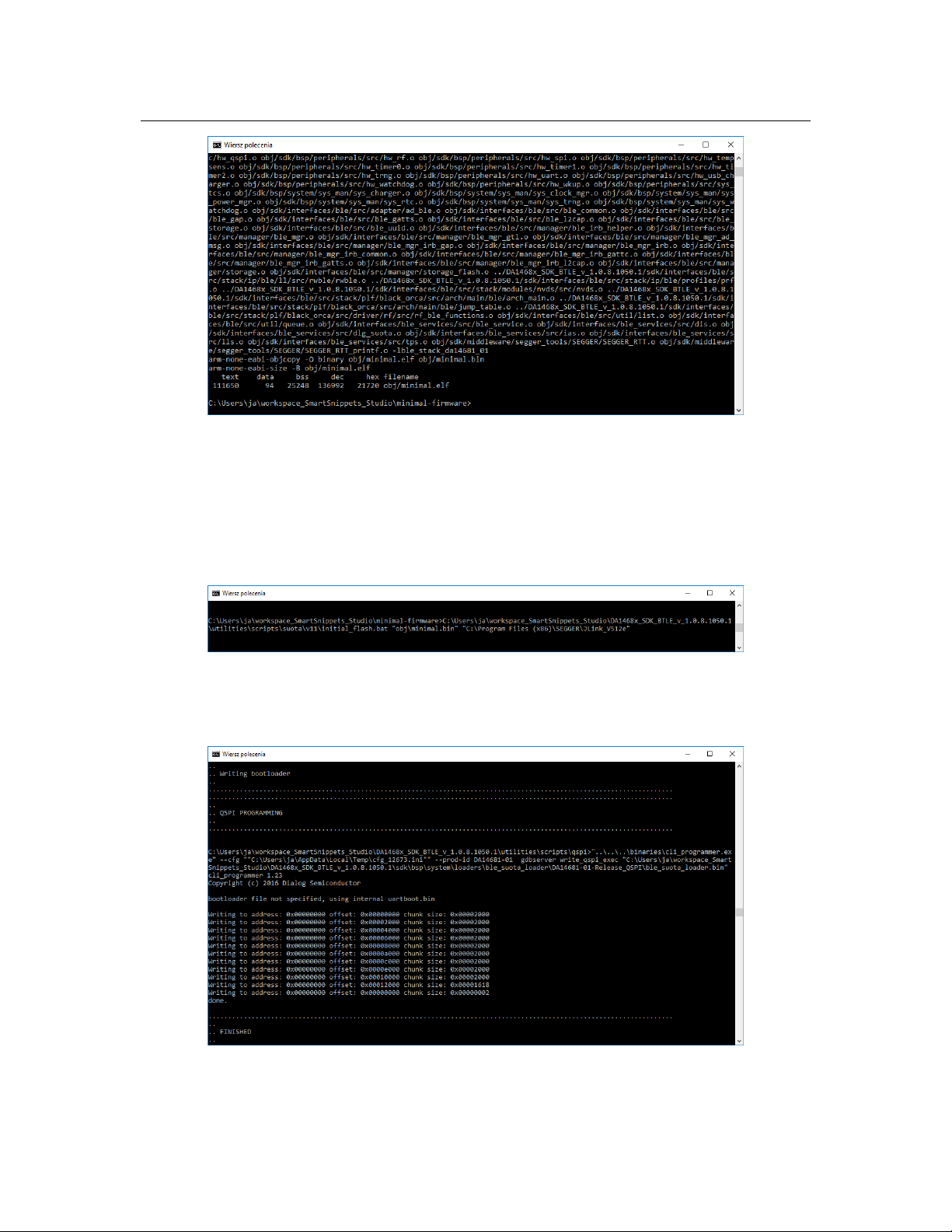
a make file which can be executed by navigating to the firmware folder and typing
command line window. This command will compile the firmware. If everything has been setup
correctly the compilation process should return no errors and a binary file should be generated as a
result, see Fugure 4.2.
After the software has been successfully compiled it can be programmed through J-Link programmer using a script provided by Dialog Semi. In command line window navigate to the DKF
folder. The programming script initial_flash.bat should be located in SDK folder:
DA1468x_SDK_BTLE_v_1.0.8.1050.1\utilities\scripts\suota\v11\
It takes two parameter - path to the .bin file with firmware and path to the J-Link tools. The syntax is
as follows:
{Path}\initial_flash.bat "{Path to firmware}" "{Path to J-Link}"
The example of the command can be seen on Figure 4.3. Before executing it the Dev Kit board has
to be powered on and J-Link programmer has to be connected to SWD port on J101. Only GND,
SWDCK and SWDIO are necessary to program the board. After successful programming process
the screen should look similar as on Figure 4.4. On default DKF configures pins 5 and 6 on the
make
in the
Page 17
4.3 Software development under Windows OS 17
Figure 4.2: Compilation process of DKF.
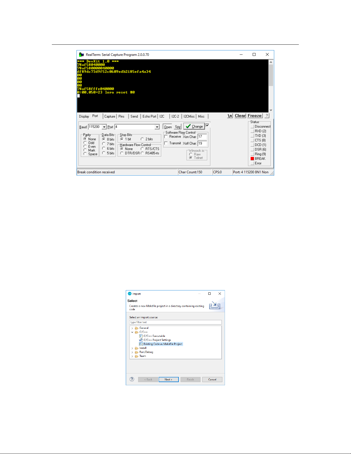
J102 connector to be UART TX and RX respectively. By connecting a UART-to-USB converter to
these pins the firmware will output the console messages. The output information sent after reset
and UART configuration can be seen on Figure 4.5.
Figure 4.3: Example of programming command.
Figure 4.4: Programming completed successfully.
Page 18
18 Chapter 4. Software Development Guide
Figure 4.5: Console output of the Dev Kit after reset.
4.3.1 Using SmartSnippet Studio
As MatchX DKF is a makefile based project it is possible to port it quite easily to different IDE and
use different operating systems. SmartSnippet Studio is a Dialog Semiconductors IDE based on
Eclipse. It offers makefile project import capabilities.
In order to import the project, open the SmartSnippet IDE.The folder structure should be the
same as in previous section, both SDK and DKF should be in SmartSnippet workspace folder. Go to
File->Import and choose ’Existing Code as Makefile Project’ like on Figure 4.6.
Figure 4.6: Import makefile project window.
Page 19
4.3 Software development under Windows OS 19
Click
Next
. On the next window navigate to the DKF folder. Choose
press
Finish
. The software should be correctly imported and you should be able to compile it by
going to Project->Build All or pressing the build icon.
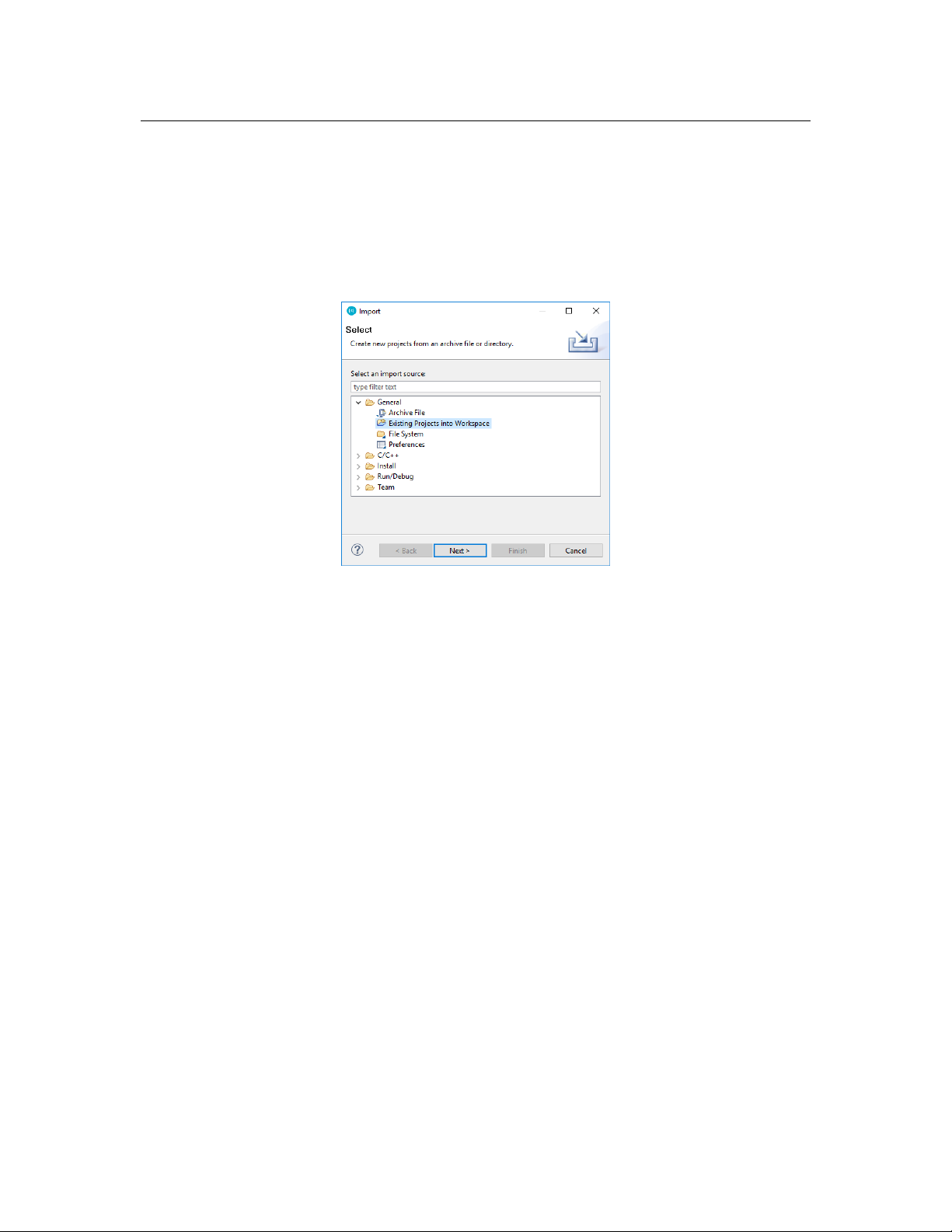
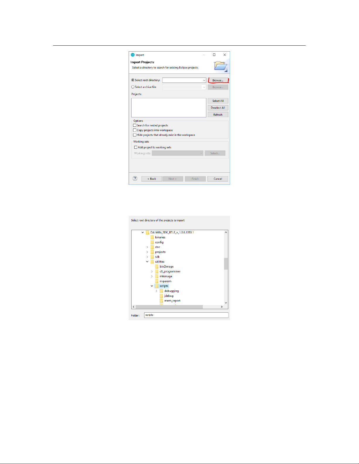
To program the just compiled firmware into DK you need to import "scripts" project to your
workspace. To do that go to
Figure 4.7.
File->Import
and choose
’Existing Projects into Workspace’
’Cross ARM GCC’
like on
and
Figure 4.7: Import existing project window.
Click
Next
. On the next window navigate to the script folder that should be located in
<sdk_root>\utilities\scripts. See Figure 4.8 and Figure 4.9
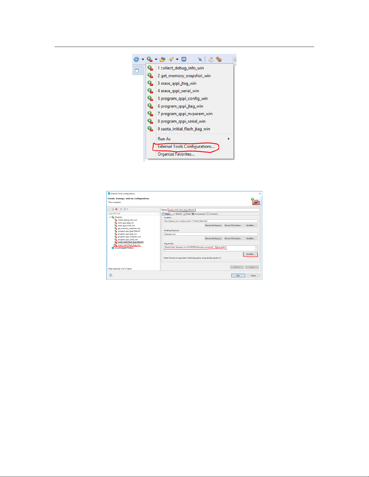
Now all the scripts should be available, but in order to use them they must be slightly modified
to point to a correct .bin file. Click on ’External Tools Configuration’ as shown on Figure 4.10.
It is best to copy the
’Duplicate’
to compiled firmware. The variables values can be modified by clicking
compiled .bin file is stored in obj folder in the project directory.
then renaming it. The
’suota_initial_flash_jtag_win’
’Argument’
section has to be modified to contain correct path
script by right clicking on it and pressing
’Variables’
button. The
Page 20
20 Chapter 4. Software Development Guide
Figure 4.8: Importing eXisting project browse window.
Figure 4.9: Browse window.
4.4 Software development under Linux
Software developing under Linux operating system is straight forward. The easiest way to setup the
environment is to install the the SmartSnippet Studio from Dialog and following the installation
guide in
DA1468x SDK (in the example the SDK version 1.0.8.1050.1 has been used) and MatchX Dev Kit
Frmware. Both SDK and Dev Kit Firmware should be put in one folder (for example SmartSnippet
workspace folder). Open the terminal and navigate to DKF folder. The project contains make file
UM-B-057
User guide from Dialog. Download the Dialog’s Semiconductor SmartSnippets
Page 21
4.5 Setting DevEUI, AppEUI and DevKey 21
Figure 4.10: Scripts.
Figure 4.11: Scripts editing.
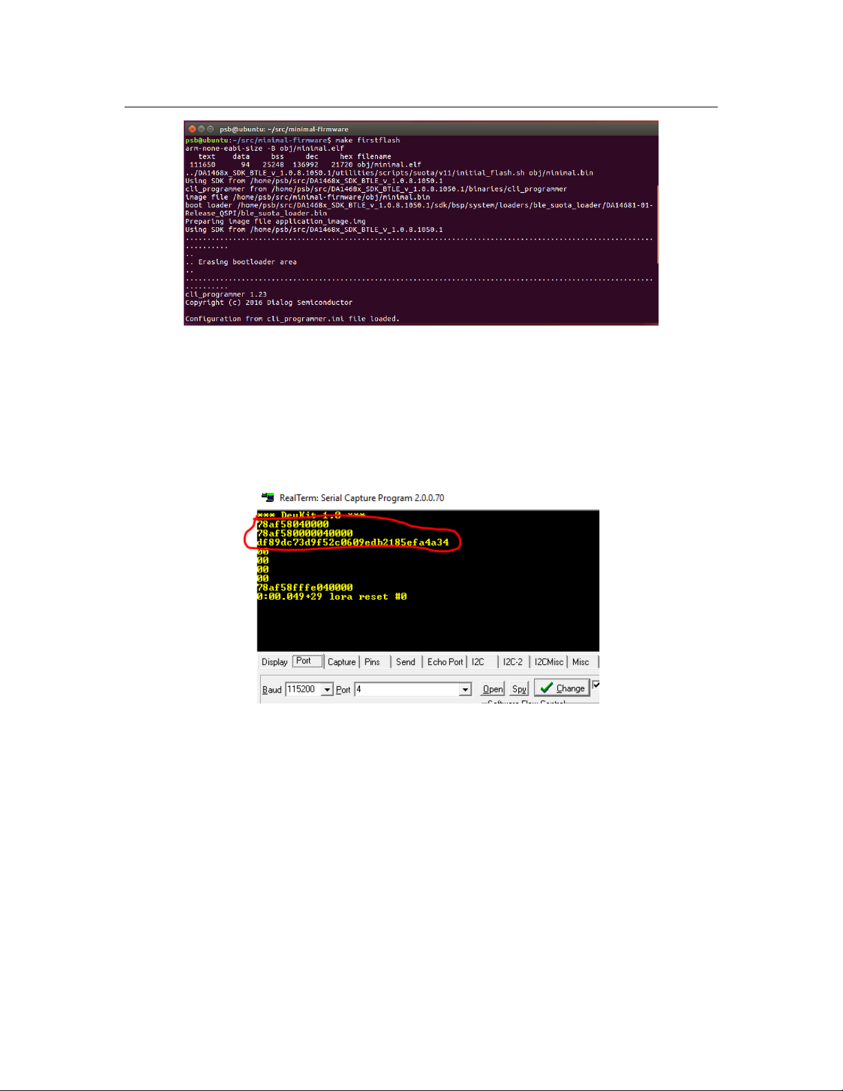
that takes over the compilation process. The firmware will be compiled by invoking
Programming the DK board is done by invoking make command with firstflash parameter.
make
4.5 Setting DevEUI, AppEUI and DevKey
To ensure the highest level of security in LoRaWAN network and Over the Air Activation (OTTA) 3
different keys have to be programmed into every end node.
• DevEUI
the end-device, also used by Bluetooth. It is converted to IEEE EUI64 by inserting 0xFFFE in
the bytes 4 and 5. e.g. 78af58fffe040000
• AppEUI
the application provider (i.e., owner) of the end-device
• DevKey - 16 bytes unique AES-128 key
These keys are programmed by MatchX and stored in a special region of the nonvolatile memory
- 6 bytes global end-device ID in IEEE EUI48 address space that uniquely identifies
- 8 bytes global application ID in IEEE EUI64 address space that uniquely identifies
command.
Page 22
22 Chapter 4. Software Development Guide
Figure 4.12: Programming DK board.
of the Dialog microcontroller. They will be preserved during flashing of the new firmware, however
they will be lost by performing full flash erase. The default values are defined in
In Dev Kit Firmware the values of these keys are printed on UART console on power up, see Figure
4.13
lora\param.c
.
Figure 4.13: Displaying the keys on UART console.
The values of DevEUI, AppEUI and DevKey can also be changed from UART console by using
param command. The syntax is as follow:
param x value
where x = 0 for DevEUI, 1 for AppEUI and 2 for DevKey, value is a hexadecimal value to be
set.
When value field is not specified the command will output current value of the parameter
(except DevKey, which will not be shown).
DevKey is a AES-128 encryption key used for secure communication. It should be kept secret
and only known to the sensor owner, this is why it is recommended to not display it on the UART
Page 23

4.5 Setting DevEUI, AppEUI and DevKey 23
in a final version of the firmware by removing
recommended to change its value before registering the node on the server.
#define DEBUG
line in
param.c
file. It is also
Page 24
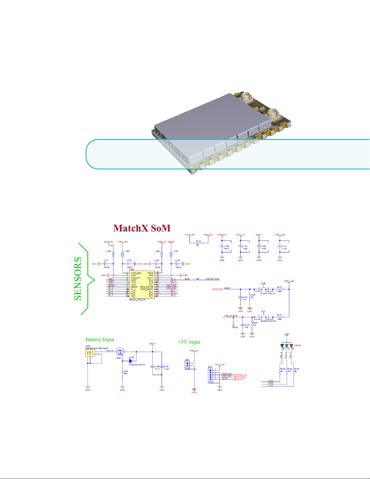
5. Typical Hardware Connection
Figure 5.1 shows the typical hardware connection.
Figure 5.1: MatchX Core reference circuit.
Page 25

5.1 Digital Interfaces 25
5.1 Digital Interfaces
Interfaces such as SPI, UART, I2C etc. can be multiplexed to any GPIO pin which gives flexibility
with sensor connection. By default P1_4 and P1_6 are used as UART console interface by MarchX
firmware.
5.2 Analog Interfaces
Pins P1_3, P1_4, P0_7, SWD_IO and SWD_CLK can be used as analog inputs to internal ADC
converter. In order to use SWD pins as analog inputs the programming and debug function of these
pins has to be disabled first in the software. It is advisable to implement some delay between reset
and disabling SWD function so the debug function can be entered after hardware reset.
Pins P1_6 and P1_4 can be also used as temperature sensing pins for battery charging and
protection. Please refer to Dialog Semiconductor DA14680 datasheet for more details.
5.3 Programming Interface
The main programming interface is Serial Wire Debug (SWD) interface comprising of SWD_IO,
SWD_CLK and optionally Reset. Additionally it is possible to use pins P1_3 and P2_3 to communicate with internal bootloader as described in UM-B-041 Production Line Tool User Manual by
Dialog Semiconductors. This interface can be used with Dialog software and Production Line Tool
to perform firmware flashing and production testing.
5.4 Antenna connection
The MX1721 Core module has been tested and certified with MatchX MX1733 Development board
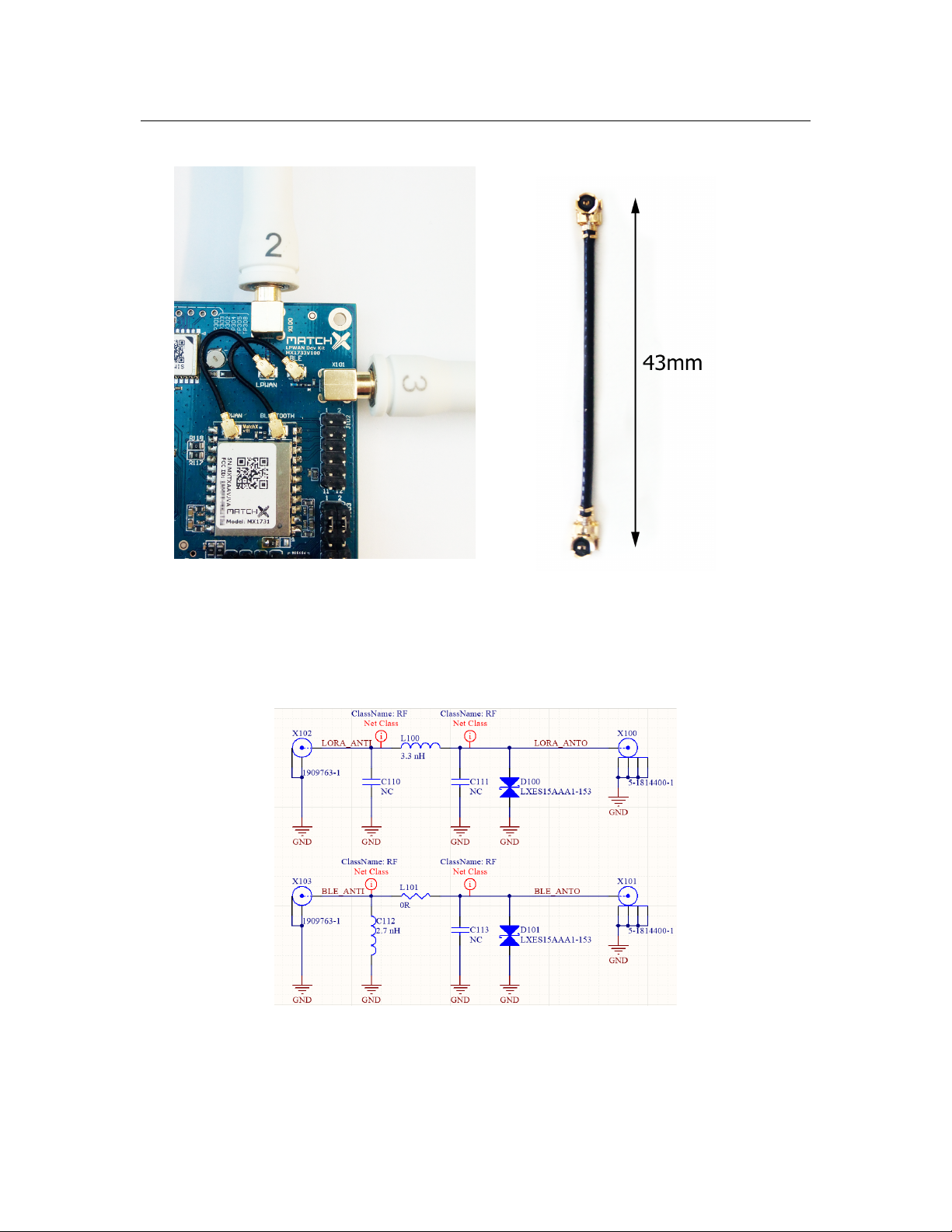
(Dev Kit). The Dev Kit is using two SMA connectors to connect external dipole antennas and two
U.FL connectors to connect RF signal from Core module. The connection is shown on Figure 5.2.
To connect the Core module to the antenna port two coaxial U.FL to U.FL pigtail cables of the length
of 43mm are used (shown on Figure 5.3).
Between U.LF and SMA connectors on the Dev kit there are few passive components for
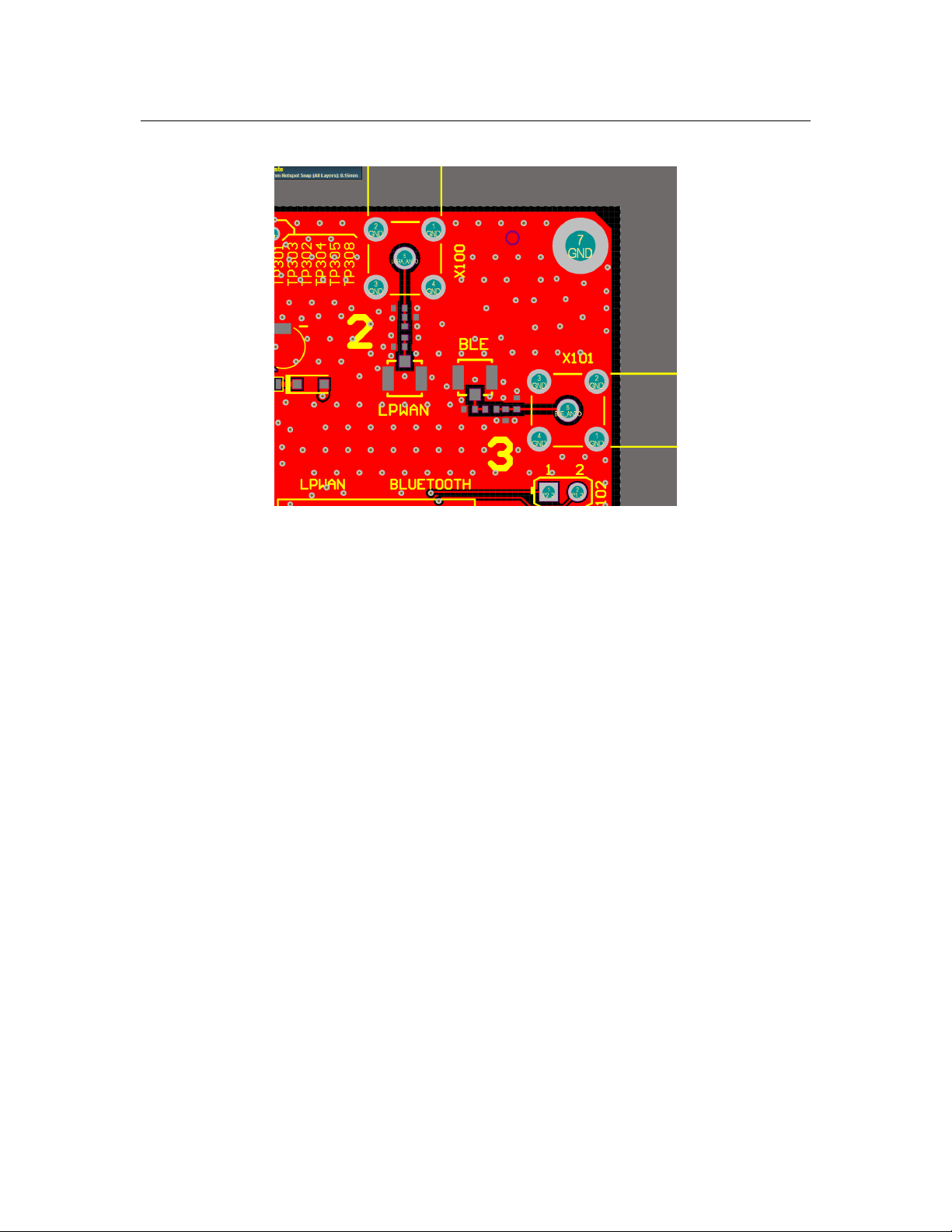
matching and ESD protection. The detailed schematic can be seen on Figure 5.4 and layout on
Figure 5.5 (the details about the Dev Kit boards, together with schematics and gerber files can be
found on the company websites
components have 0402 size. The matching circuit has been designed in the way to match the antenna
to 50Ohm impedance.
www.matchx.io
). All inductors, capacitors, resistors and ESD
Page 26
26 Chapter 5. Typical Hardware Connection
Figure 5.2: MatchX Core reference connection.
Figure 5.4: MatchX Core antenna connection circuit.
Figure 5.3: RF cable size.
Page 27
5.4 Antenna connection 27
Figure 5.5: MatchX Core reference circuit.
Page 28
6. Product specification
The MatchX Core SoM is designed for enhanced LPWAN performance and manageability. In this
chapter we briefly introduce the specifications for both hardware and software.
6.1 Hardware environment
The Core Module is designed to make design process of smart connected LPWAN devices as easy
as possible. It can be easily incorporated into existing solution or be a core controlling unit for
new design. Together with MatchX Dev Kit hey help to kickstart your project by providing test
and evaluation hardware for proof of concept and enable programmers to develop software before
custom hardware is ready.
Item Description
MCU DA14680, 0 Hz up to 96 MHz 32-bit ARM Cortex-M0
Memory 8Mb Flash, 64kB OTP, 128kB ROM, 144kB SRAM
Interfaces I2C, I2S, PCM, SPI, UART, GPIOs
Wireless Bluetooth 4.1 and LoRa
Battery Li-poly battery charging and managing system
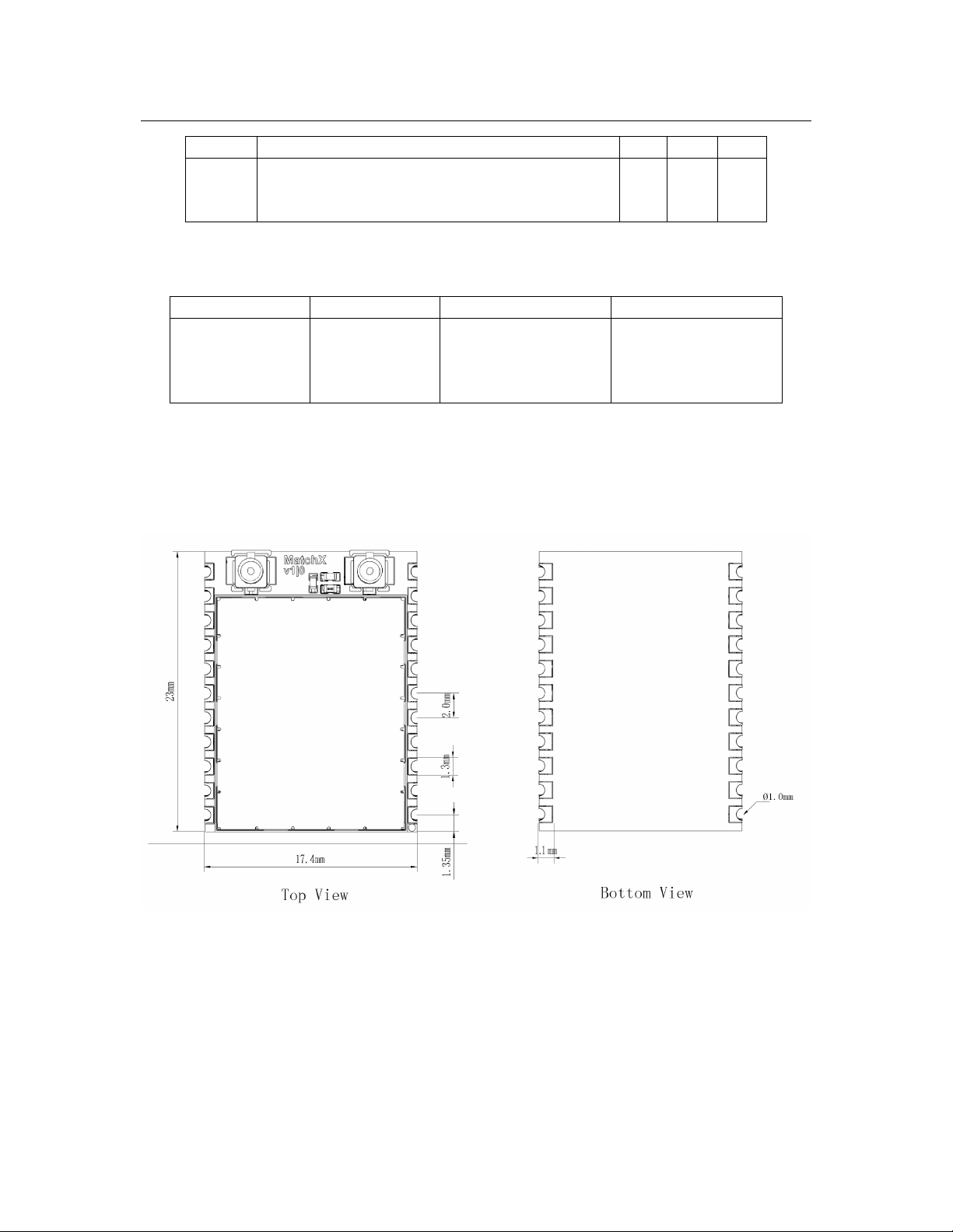
Size 23 x 17.4 x 3mm
Table 6.1: Key hardware specifications
.
6.2 Software environment
To facilitate an easy network deployment, we have included many software features, which include
but are not limited to:
• Open source SDK and software support
Page 29
6.3 RF performance 29
• Over The Air software update
• Mobile App for Android and iPhone smartphones
• Free cloud service for managing and visualizing sensors data
6.3 RF performance
There are two RF systems in the module, which include Lora, and Bluetooth. In this section we
briefly introduce the performance of these systems. For Lora, both the "transmission" and "receive"
performance are listed in Table 6.2 and "Bluetooth" can be found in Table 6.3.
Item Value
TX Max +18dBm
RX down to -148dBm
Table 6.2: Lora RF performance
For Bluetooth is listed in Table 6.3.
Item Value
Output Power 0dBm
Sensitivity -94dBm
Table 6.3: Bluetooth performance.
6.4 Electrical characteristics
Symbol Description Min Max Unit
V
BATT
V3P3
I
V 3P3
V
GPIO
V
BUS
I
BUS
T
op
LDO
Battery voltage 2.7 4.2 V
Voltage output on the internal LDO V
LDO
BATT
3.3 V
Current output of 3V3_SNR 0 100mA mA
Voltage on any GPIO pin 0 V3P3
USB charging voltage 4.2 5.75 V
USB charging current supply 300 mA
Operating Temperature -40 +85
LDO
V
◦
Table 6.4: Operating Range.
6.5 Antenna characteristics
The SoM module is equipped with two U.FL connectors: 2.4GHz for Bluetooth and one for 868MHz
(915MHz in US version) LoRa antenna. The parameters of the recommended antennas can be found
in Table 6.6. It is recommended to use dipole antennas as they are less susceptible to ground plane
size and are less prone to detuning by surrounding objects.
C
Page 30
30 Chapter 6. Product specification
Symbol Description Min Max Unit
I
IDLE
I
SEN D
I
SLE E P
Current consumption, MCU awake, no RF activity 10 mA
Current consumption,sending LoRa packet 75 mA
Current consumption in sleep mode <10 µA
Table 6.5: Current consumption.
Parameter 2.4GHz antenna 868MHz (EU version) 915MHz (US version)
Center Frequency 2.44GHz 868MHz 915MHz
Bandwidth 101MHz 40MHz 40MHz
Gain 3dBi 2.5dBi 2.5dBi
Type Dipole Dipole Dipole
Table 6.6: Parameters of recommended antennas.
6.6 Dimensions
Figure 6.1: Dimension of the SoM module, all dimensions in mm.
Page 31
6.6 Dimensions 31
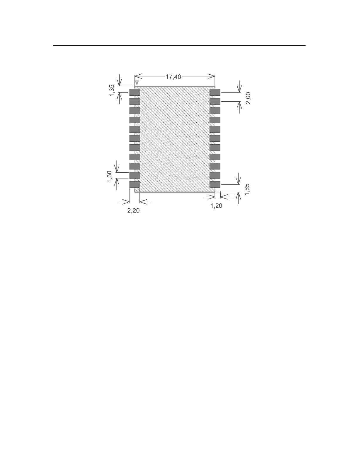
Figure 6.2: Recommended footprint (top view), all dimensions in mm.
Page 32
7. Certification
This section outlines the regulatory information for the MX1731 module for the following coun-
tries/regions:
• United States
• EU
7.1 FCC
This device complies with Part 15 of the FCC Rules. Operation is subject to the following two
conditions:
(1) This device may not cause harmful interference.
(2)
This device must accept any interference received, including interference that may cause
undesired operation.
NOTE:
device, pursuant to part 15 of the FCC Rules. These limits are designed to provide reasonable
protection against harmful interference in a residential installation. This equipment generates
uses and can radiate radio frequency energy and, if not installed and used in accordance with
the instructions, may cause harmful interference to radio communications. However, there is no
guarantee that interference will not occur in a particular installation. If this equipment does cause
harmful interference to radio or television reception, which can be determined by turning the
equipment off and on, the user is encouraged to try to correct the interference by one or more of the
following measures:
– Reorient or relocate the receiving antenna.
– Increase the separation between the equipment and receiver.
–
– Consult the dealer or an experienced radio/TV technician for help.
NOTE:
rized modifications to this equipment. Such modifications could void the users authority to operate
This equipment has been tested and found to comply with the limits for a
Connect the equipment into an outlet on a circuit different from that to which the receiver is
connected.
The manufacturer is not responsible for any radio or TV interference caused by unautho-
Class B
digital
Page 33

7.1 FCC 33
the equipment.
This equipment complies with FCC radiation exposure limits set forth for an uncontrolled environment. This equipment should be installed and operated with minimum distance of 20 cm between
the radiator and your body. This transmitter must not be co-located or operating in conjunction with
any other antenna or transmitter.
ORIGINAL EQUIPMENT MANUFACTURER (OEM) NOTES
The OEM must certify the final end product to comply with unintentional radiators before declaring
compliance of the final product to Part 15 of the FCC rules and regulations. Integration into devices
that are directly or indirectly connected to AC lines must add with Class II Permissive Change.
The OEM must comply with the FCC labeling requirements. If the modules label is not visible
when installed, then an additional permanent label must be applied on the outside of the finished
product which states:
“Contains transmitter module FCC ID: 2AMPF-MX1731".
Additionally, the following statement should be included on the label and in the final products user
manual:
“This device complies with Part 15 of the FCC Rules. Operation is subject to the following two
conditions:
(1) This device may not cause harmful interference, and
(2)
this device must accept any interference received, including interference that may cause
undesired operation.”
The module is limited to installation in mobile or fixed applications. Separate approval is required
for all other operating configurations, including portable configuration with respect to Part 2.1093
and different antenna configurations.
Professional installation:
When they have not been tested and granted in this manner, additional testing and/or FCC application
filing may be required. The most straightforward approach to address additional testing conditions is
to have the grantee responsible for the certification of at least one of the modules submit a permissive
change application.
When having a module grantee file a permissive change is not practical or feasible, the following
guidance provides some additional options for host manufacturers. Integrations using modules where
additional testing and/or FCC application filing(s) may be required are: (A) a module used in devices
requiring additional RF exposure compliance information (e.g., MPE evaluation or SAR testing);
(B) limited and/or split modules not meeting all of the module requirements; and (C) simultaneous
transmissions for independent collocated transmitters not previously granted together.
This Module is limited modular approval, it is limited to OEM installation ONLY. Integration
into devices that are directly or indirectly connected to AC lines must add with Class II Permissive
Change. (OEM) Integrator has to assure compliance of the entire end product include the integrated
Module.
Additional measurements (15B) and/or equipment authorizations (e.g Verification) may need to
be addressed depending on co-location or simultaneous transmission issues if applicable. (OEM)
Integrator is reminded to assure that these installation instructions will not be made available to the
end user of the final host device.
Page 34

34 Chapter 7. Certification
7.1.1 Antenna information
To maintain modular approval in the United States, only the antenna types that have been tested shall
be used.It is permissible to use different antenna manufacturer provided the same antenna type and
antenna gain (equal to or less than) is used. Testing of the MX1731 module was performed with the
antenna types listed in Table 6.6.
7.2 CE
RF exposure information: The Maximum Permissible Exposure (MPE) level has been calculated
based on a distance of 20 cm between the device and the human body. To maintain compliance with
RF exposure requirement, use product that maintain a 20cm distance between the device and human
body.
Hereby,
Directive 2014/53/EU. The full text of the EU declaration of conformity is available at the following
internet address:
MatchX GmbH
www.matchx.io
declares that the radio equipment type
.
MX1731
is in compliance with
Page 35
8. Important Notice
The information contained herein is believed to be reliable. MatchX makes no warranties regarding
the information contained herein. MatchX assumes no responsibility or liability whatsoever for any
of the information contained herein. MatchX assumes no responsibility or liability whatsoever for
the use of the information contained herein. The information contained herein is provided "AS IS,
WHERE IS" and with all faults, and the entire risk associated with such information is entirely with
the user. All information contained herein is subject to change without notice. Customers should
obtain and verify the latest relevant information before placing orders for MatchX products. The
information contained herein or any use of such information does not grant, explicitly or implicitly,
to any party any patent rights, licenses, or any other intellectual property rights, whether with regard
to such information itself or anything described by such information.
MatchX products are not warranted or authorized for use as critical components in medical,
life-saving, or life-sustaining applications, or other applications where a failure would reasonably be
expected to cause severe personal injury or death.
 Loading...